|
|
|
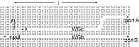
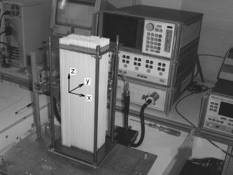
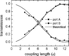
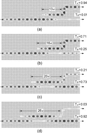
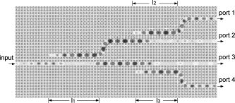
Photonic crystals (PCs) are artificially engineered materials with periodic arrangement of dielectric constants.1 They prohibit propagation of light for frequencies within the photonic band gaps. The PC has opened up a new way to control light and construct integrated optical circuits. Many optical devices based on PCs have been proposed, e.g., optical couplers, filters, and microcavity lasers. 2D PCs are widely adopted because of the difficulty in fabricating 3D PCs. An index-guiding mechanism is utilized in the vertical direction to eliminate out-of-plane losses in 2D PC structures.2 The power splitter is one of the most important components of the integrated optical systems. The typical power splitter built on PC with a Y-junction structure3 has a poor transmission. The directional coupling has been used to design high efficient power splitters. The performance of the PC waveguide directional coupler has been experimentally demonstrated by Cuesta at microwave frequencies for a PC with a triangular arrangement of dielectric rods in air.4 In the coupling region, the single mode in the isolated waveguide splits into two guided modes with odd and even symmetries with respect to the plane equidistant from both waveguides. The odd and even modes have different propagation constants: and , respectively. As a result, the electromagnetic power fully shifts from one guide to another after propagating a distance of and then turns back to the first guide after the same distance. An efficient power splitter based on PC waveguide directional coupling has been designed with a mechanism similar to the conventional three-waveguide directional couplers.5 However, each of the two output power is fixed to about half of the input power because of the symmetry structure. In this work, we propose a novel power splitter based on PC waveguide directional coupling that provides different levels of output power. The dependence of the transmission on the length of directional coupling region is presented. The experimental results are compared with the theoretical ones, and good correspondences between them will be shown. In our calculation, a supper cell of is taken to calculate the dispersion curve by utilizing the plane wave method (PWM),6 where is the lattice constant. The finite-domain time-difference (FDTD) scheme7 implemented with PC-based perfectly matched layers (PC-PMLs)8 is employed to simulate the wave propagation and to calculate the transmission spectrum. The bulk PC is defined by a square arrangement of dielectric rods in air. The dielectric constant of the rod is and the radius is . Such parameters provide a band gap of for E-polarized wave. First, we investigate a power splitter with two branches as shown in Fig. 1. It is designed by creating a bend waveguide WGc beside a straight one labeled WGb. The distance between the paralleling waveguides is 2 PC lattices. The bend with very high transmission is employed to greatly reduce the bend loss.9 Directional coupling occurs within the parallel region of these two waveguides. The input single mode splits into one odd and one even mode. Figure 2 shows the dispersion relations of the input single mode and the coupling modes. and are obtained by employing the PWM with 1521 plane waves. They are symmetric with respect to the propagation constant of the single mode. Because of the structural symmetry in the coupling region, each of the parallel waveguides carries the same quantity of power, and the amplitudes of the odd and even modes are also equal to each other. Therefore, the amplitudes of the odd and even modes are both , where is the amplitude of the input mode. Furthermore, the intensity at the left end of coupling region in WGc is always zero, that is, there is a phase difference of between odd mode and even mode at that position. The wave function in WGc can be obtained with , where and are wave functions of odd and even modes in WGc, and they can be expressed as: where . Therefore, we obtain the distribution of intensity within coupling region in WGc:where is the input intensity. The intensity in WGc at the right end of coupling region will be guided around the bend and sent to the output port A. Transmission of the output port A is defined as , where is the intensity at output port A. The transmission of the output port A and B can be calculated by: where is the coupling length in unit . However, because of the discrete structure of the photonic crystal, should be rounded off to an integral times of . The influence of the discrete structure can be reduced by using a larger . Further calculation shows that increases exponentially as the distance between the parallel waveguides increases.A 2D photonic crystal in the microwave frequency regime is designed for experiments. The alumina rods, which are in length and in diameter, are arranged in a square lattice array with a lattice constant of . As shown in Fig. 3, a network analyzer is used to measure the transmission spectra and two horn antennas are used as the source and detector adaptors. The horn antennas are placed directly to the input or output ports with orientations that provide electric field paralleling to the alumina rods. The port A is set along the y direction in the experimental setup, so that the signals from port A and port B can be detected separately. The measured results of the transmissions are shown in Fig. 4, and are compared with the theoretical results calculated with Eqs. 4, 5. The frequency of input microwave is 17G and is at this frequency. In order to eliminate the influence of input and output coupling efficiency, the experimental transmission of the splitter is normalized by the transmission of an isolated straight waveguide. A good correspondence between the experimental and theoretical results can be observed. The slight disagreements are caused mainly by the position disorders of alumina rods. On the other hand, the difference in group velocities of odd and even modes, which can be observed in Fig. 2, results in low cross talk in coupling properties. This is also one of the reasons for the disagreement. Figure 5 shows the field patterns calculated by FDTD for power splitters with different coupling lengths. The lengths of coupling region and the transmission for each output port are shown in Fig. 5. The input power is split into different ratios. The pulse with narrow frequency range centered at is excited by a dipole source with a Gaussian temporal profile. A total transmission of is obtained throughout the calculated coupling lengths. The loss is mainly caused by the bends of WGc. Then, by further splitting power in each branch, the number of output port can be improved. Figure 6 shows the electric field pattern in a splitter with 4 output ports. The frequency of input pulse is . The coupling lengths are , , and , respectively. is observed, where is the transmission of port port 4 in Fig. 6. In conclusion, we have proposed a novel splitter based on PC waveguide directional coupling. Different output power levels can be obtained by changing the coupling length. A high total transmission is achieved with the low-loss bends. The power in each branch can be further split to obtain more output ports. AcknowledgementsWe would like to acknowledge the support from the National Natural Science Foundation of China under Grant No. 10475048. ReferencesJ. D. Joannopoulos,
R. D. Meade, and
J. N. Winn, Photonic Crystals: Molding the Flow of Light,
(1995) Google Scholar
S. G. Johnson,
S. H. Fan,
P. R. Villeneuve, and
J. D. Joannopoulos,
“Guided modes in photonic crystal slabs,”
Phys. Rev. B, 60
(8), 5751
–5758
(1999). https://doi.org/10.1103/PhysRevB.60.5751 0163-1829 Google Scholar
S. Boscolo,
M. Midrio, and
T. F. Krauss,
“Y junction in photonic crystal channel waveguides: high transmission and impedance matching,”
Opt. Lett., 27
(12), 1001
–1003
(2002). 0146-9592 Google Scholar
F. Cuesta,
A. Griol,
A. Martinez, and
J. Marti,
“Experimental demonstration of photonic crystal directional coupler at microwave frequencies,”
Electron. Lett., 39
(5), 455
–456
(2003). https://doi.org/10.1049/el:20030317 0013-5194 Google Scholar
I. Park,
H. -S. Lee,
H. -J. Kim,
K. -M. Moon,
S. -G. Lee,
B. -H. O,
S. -G. Park, and
E. -H. Lee,
“Photonic crystal power-splitter based on directional coupling,”
Opt. Express, 12
(15), 3599
–3604
(2004). https://doi.org/10.1364/OPEX.12.003599 1094-4087 Google Scholar
K. M. Ho,
C. T. Chan, and
C. M. Soukoulis,
“Existence of a photonic gap in periodic dielectric structures,”
Phys. Rev. Lett., 65
(25), 3152
–3155
(1990). https://doi.org/10.1103/PhysRevLett.65.3152 0031-9007 Google Scholar
K. S. Yee,
“Numerical solution of initial boundary value problems involving Maxwell’s equations in isotropic media,”
IEEE Trans. Antennas Propag., AP-14
(3), 302
–307
(1966). https://doi.org/10.1109/TAP.1966.1138693 0018-926X Google Scholar
M. Koshiba,
Y. Tsuji, and
S. Sasaki,
“High-performance absorbing boundary conditions for photonic crystal waveguide simulations,”
IEEE Microw. Wirel. Compon. Lett., 11
(4), 152
–154
(2001). 1531-1309 Google Scholar
A. Mekis,
J. C. Chen,
I. Kurland,
S. H. Fan,
P. R. Villeneuve, and
J. D. Joannopoulos,
“High transmission through sharp bends in photonic crystal waveguides,”
Phys. Rev. Lett., 77
(18), 3787
–3790
(1996). https://doi.org/10.1103/PhysRevLett.77.3787 0031-9007 Google Scholar
|