
|
|
|
Optical coherence imaging is a biomedical optical imaging tool based on a low-coherence interferometer structure that is used to obtain cross-sectional images of highly scattering samples with resolutions in the micrometer range.1 Such images are reconstructed by recording and processing the interference of backscattered and/or backreflected light from the sample with reference light backreflected from a retroreflector. Scanning the position of the reference retroreflector, which may be performed by a linear translational stage, varies the optical range in the sample from which light scattered or backreflected can interfere with the reference light. The moving retroreflector induces a Doppler frequency shift in the reference light, which is given by , where is the speed of the translational stage and is the source center wavelength. When the Doppler-shifted reference light is recombined with the sample light at the beam splitter of the interferometer to produce interference at the photodetector, the Doppler shift is transferred to the frequency of the generated electrical signal. The signal obtained can also be modulated by an external phase modulator, such as a piezoelectric fiber stretcher,2 and piezo-stack.3 The detection electronics that amplifies the signal and conducts the demodulation is required in time domain (TD) optical coherence imaging for medical and biologic applications to obtain high sensitivity. The demodulation process can occur by either mixing or envelope detection. Envelope detection is more advantageous than mixing when the phase or frequency of the carrier has nonlinear variations, for example, due to nonlinear sweeping of the reference mirror or nonlinear frequency chirping.4 Such nonlinear variations are common in Fourier domain (FD) optical delay lines used in TD optical coherence high-speed imaging. The instrumentation and the optimization of an optical coherence imaging system are challenging.5 Logarithmic amplifiers,6 RMS voltmeters,3 analog CMOS circuits based on mixing for demodulation,7 and field-programmable gate arrays (FPGA)8 have been employed in various optical coherence imaging systems for signal processing after photodetection. In this letter, we demonstrate compact low-cost demodulating envelope detection electronics with monolithic integrated-circuit active filters and demodulating logarithmic amplifier. Although FD optical coherence imaging has a typical sensitivity advantage over TD optical coherence imaging, to fully exploit the advantage of FD optical coherence imaging, an expensive and bulky CCD camera with a cooling system should be used to reach the shot noise limit.9 The TD optical coherence imaging with a compact and low-cost detection scheme can be applied to field applications requiring portability over highest sensitivity. We implemented a fiber-based imaging system with single-mode fiber, as shown in Fig. 1. The light source illuminating the system is a superluminescent diode (Superlum D930-HP) centered at with bandwidth. Two custom-designed broadband fiber couplers that can support the large bandwidth of the light source were employed in the system to enable the dual-balanced detection of the interference signal. Fig. 1Schematic of the TD optical coherence imaging system implemented with dual-balanced detection. Superluminescent Diode (SLD), Fiber coupler (FC), piezoelectric phase modulator (PM). 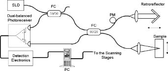 A gold-coated retroreflector placed on a linear stage that can scan as fast as provided depth scanning of the sample, while a second stage was employed for transversal scanning. The returning phase-modulated reference light was recombined with the light scattered or backreflected from the sample at the 80/20 fiber coupler. While a part of the recombined light was directed to one of the two photodiodes in the dual-balanced photoreceiver (Nirvana Model 2017), the rest returned to the fiber coupler, where it was split to reach the other photodiode. The dual-balanced detection technique was chosen to eliminate intensity noise of the light source. A detection electronics that serves to filter out-of-band noise components in the signal detected by the dual-balanced photoreceiver and to perform demodulation follows the dual-balanced photoreceiver. The signal generated with the system shown in Fig. 1 was phase modulated at . We designed and implemented custom electronics comprising a bandpass filter followed by a demodulating logarithmic amplifier, a low pass filter, and a single-ended-to-differential amplifier in cascaded configuration. The bandpass filter is a 4th order Butterworth bandpass filter with two cascaded universal active filters (Burr Brown UAF42) that implement a Kerwin-Huelsman-Newcomb (KHN) biquad topology. The UAF42 filters operate in the frequency range between 0 to and can be configured to realize Butterworth, Chebyshev, and Bessel filter types. The center frequency of the filter was set to , with a bandwidth that can cover a signal bandwidth set by a scanning speed of up to . The demodulating logarithmic amplifier is also an integrated circuit (Analog Devices AD606). The output of a logarithmic amplifier is the logarithm of the input signal’s envelope,10 but with characteristic rectifier-type ripples that need to be removed with low pass filtering. Thus a low pass filter stage was implemented with additional UAF42s with cutoff frequency of . At the final stage, additional conversion gain was added by a single-ended-to-differential amplifier (Analog Devices AD8138). In Fig. 2, we show the input waveform ( ) together with output waveforms with and without the low pass filtering stage ( and ) after the logarithmic amplifier. Fig. 2Input and corresponding output waveforms after the designed demodulator when the low-pass filter after logarithmic amplifier is switched off and switched on . 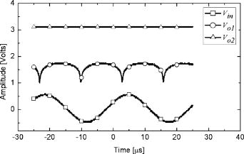 The conversion formula for the detection electronics system was obtained to be , where is the amplitude of the modulated input signal and is the output of the detection electronics. The circuit was implemented on a small four-layer printed circuit board with the size of . To quantify the sensitivity of the imaging system when the new detection electronics was employed, we used an OD1.2 filter followed by a mirror in the sample arm of the setup shown in Fig. 1. The controlled attenuation provided the information that the signal peaked at reflectivity as the sample arm beam passed twice through the OD1.2 filter. Figure 3a shows the recorded signal. We also scanned the same sample configuration using a lock-in amplifier (Stanford Research SR830) for comparison with our compact detection circuit. Figure 3b shows the signal recorded with the lock-in amplifier. The time constant of the lock-in amplifier was set to , which corresponds to a 1.59-kHz low pass filter bandwidth that is equivalent to the bandwidth of the designed detection electronics. Fig. 3Signals recorded using (a) custom-designed logarithmic amplifier-based detection electronics and (b) lock-in amplifier. 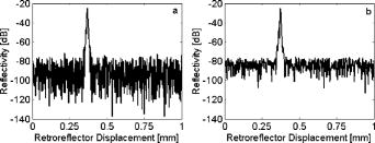 The sensitivity of the imaging system is given by where is the peak voltage of the signal and is the standard deviation of the signal noise floor. The system sensitivity we obtained with the custom-designed detection electronics was , compared to with the lock-in amplifier.Figure 4a presents the image of a fresh onion recorded with the designed detection electronics. In Fig. 4b, we show the onion image when a lock-in amplifier is used. The implemented imaging system provides axial resolution in air. Due to the nature of the logarithmic amplifier, the images obtained with the custom designed demodulator are in log-scale. However, the output of the lock-in amplifier is in linear scale, and therefore such images were converted to log-scale after data acquisition. The images are . No image averaging or image processing methods were applied. The polygonal structure of the onion sample is clearly visible in both images. Fig. 4Images of fresh-onion sample recorded with (a) custom-designed logarithmic amplifier-based detection electronics and (b) lock-in amplifier. 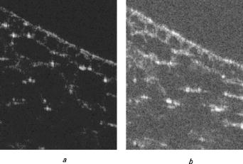 In this letter, we analyze the signal processing stage in optical coherence imaging systems. While the optics of the imaging system set the limits for performance characteristics such as axial and lateral resolution, the sensitivity of the system depends on the detection electronics. We demonstrate the feasibility of a compact and low-cost detection electronics implemented by a few integrated circuits (ICs) that filter, demodulate, and amplify the signal. While commercial lock-in amplifiers have the advantage of being tunable over a wide range of frequencies, which has value for optimization across various applications (e.g., real-time in vivo biomedical imaging versus in vitro biological imaging), the detection electronics we designed is targeted to operate purposely at fixed modulation frequency and signal bandwidth for in vitro or in-the-field biological imaging to achieve a compact and low-cost solution for portable imaging units. We demonstrate that the portable unit provides an equivalent performance to the lock-in amplifier. AcknowledgmentsThe authors thank Huikai Xie for stimulating discussion about this work. The research was funded under the National Science Foundation, the Defense Advanced Research Projects Agency Photonics Technology Access Program, and the Florida Photonics Center of Excellence. ReferencesD. Huang,
E. A. Swanson,
C. P. Lin,
J. S. Schuman,
W. G. Stinson,
W. Chang,
M. R. Hee,
T. Flotte,
K. Gregory,
C. A. Puliafito, and
J. G. Fujimoto,
“Optical coherence tomography,”
Science, 254 1178
–1181
(1991). 0036-8075 Google Scholar
M. Sato,
K. Seino,
K. Onodera, and
N. Tanno,
“Phase-drift suppression using harmonics in heterodyne detection and its applications in optical coherence tomography,”
Opt. Commun., 184 95
–104
(2000). https://doi.org/10.1016/S0030-4018(00)00930-5 0030-4018 Google Scholar
B. M. Hoeling,
A. D. Fernandez,
R. C. Haskell,
E. Huang,
W. R. Meyers,
D. Petersen,
S. E. Ungersma,
R. Wang,
M. E. Williams, and
S. E. Frasier,
“An optical coherence microscope for 3-dimensional imaging in developmental biology,”
Opt. Express, 6 136
–146
(2000). 1094-4087 Google Scholar
B. E. Bouma and
G. J. Tearney,
“Optical coherence tomography: theory,”
Handbook of Optical Coherence Tomography, 41
–66 Marcel Dekker, New York (2002). Google Scholar
J. P. Rolland,
J. O'Daniel,
A. C. Akcay,
T. DeLemos,
K. Lee,
K. Cheong,
E. Clarkson,
R. Chakabarti, and
R. Ferris,
“Task-based optimization and performance assessment in optical coherence imaging,”
J. Opt. Soc. Am. A, 22 1132
–1142
(2005). 0740-3232 Google Scholar
A. I. Kholodnykh,
I. Y. Petrova,
M. Motamedi, and
R. O. Esenaliev,
“Accurate measurement of total attenuation coefficient of thin tissue with optical coherence tomography,”
IEEE J. Sel. Top. Quantum Electron., 9 210
–221
(2003). 1077-260X Google Scholar
R. Kariya,
D. L. Mathine, and
J. K. Barton,
“Analog CMOS circuit design and characterization for optical coherence tomography signal processing,”
IEEE Trans. Biomed. Eng., 51 2160
–2163
(2004). 0018-9294 Google Scholar
A. W. Schaefer,
J. J. Reynolds,
D. L. Marks, and
S. A. Boppart,
“Real-time digital signal processing-based optical coherence tomography and Doppler optical coherence tomography,”
IEEE Trans. Biomed. Eng., 51 186
–190
(2004). https://doi.org/10.1109/TBME.2003.820369 0018-9294 Google Scholar
M. Choma,
M. Sarunic,
C. Yang, and
J. Izatt,
“Sensitivity advantage of swept source and Fourier domain optical coherence tomography,”
Opt. Express, 11 2183
–2189
(2003). 1094-4087 Google Scholar
E. Nash,
“Ask the applications engineer—28, logarithmic amplifiers explained,”
Analog Dialogue, 33
(3), 1
–5
(1999). Google Scholar
|


