|
|
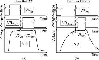
1.IntroductionPolarity inversion methods in active matrix liquid crystal displays (AMLCDs) have been developed for consideration of image quality, crosstalk, power-consumption, flicker, and so on. A dot inversion or pixel inversion is considered the best inversion method from the viewpoint of image quality.1 However, most LCD panels for monitors and laptop computer displays adopt a two-line inversion with a one-line offset, as shown in Fig. 1. To cut the costs of an LCD panel, reduced mask-count processes were developed for monitors and laptop computer displays.2 But, horizontal-line defects on an LCD panel driven by two-line inversion are observed due to more resistive data bus lines. The two adjacent pixels in a column should be driven by a single voltage level with the same polarity when the pixels have the same digital image data. Figure 2 shows two row signals for even and odd rows, and , and one column signal, VC, for the two-line inversion when the two pixel image data are the same. A voltage level of the column signal when a row signal falls to an off-level determines the voltage of a pixel located at both the row and column. If the charging time of the column line is not sufficient, then the column signal shows a delayed waveform, as shown in Fig. 2. A voltage difference at the falling transition points, as shown in Fig. 2, may cause a luminance difference between the two neighboring pixels. Thus, we can observe the horizontal failure lines. If an LCD is driven by higher refresh rates such as 75, 85, or , the LCD may show the same failure due to insufficient time to charge column lines. In this work, I propose an on-time modulation (OTM) method to overcome the insufficient time for charging column lines. Fig. 1Spatial polarity arrangement in an LCD panel driven by the two-line inversion with one-line offset.  Fig. 2Even and odd row signals ( and ) and one column signal (VC) for the two-line inversion shown in Fig. 1.  2.On-Time ModulationAs shown in Fig. 1, the polarity of every even pixel is opposite to that of the previous odd pixel. Hence, all even pixels suffer from insufficient charging time. The main idea of the OTM is to extend turn-on times of even row signals and to reduce pulse widths of the next odd rows by the same amount of time extended at the previous even rows. Figure 3 shows two row signals for the OTM and a column signal according to the positions from a column driver (CD). I express the voltage level of the column signal when an even (or odd) row signal falls to the off-level as (or ), illustrated by an open circle (or open square) shown in Fig. 3. Figure 3a shows row and column signals for the pixels near to the CD. and are almost the same, because the pixels are close to the CD and a delay of the column signal is small. Thus, unwanted horizontal lines are not observable near the CD. Figure 3b shows the row and column signals far from the CD. Due to a higher load of the column line, the delay of the column signal becomes bigger. Hence, has a much lower level than . By extending the on-time of the even pixel as shown in Fig. 3, an adjusted column voltage , illustrated by a solid circle, becomes comparable to . The compensated turn-on time of the row signal makes it possible to balance the column voltages of the two adjacent pixels. As a result, the OTM can get rid of the horizontal defect lines far from the CD. 3.Experimental ResultsFor the experiment, a 17-in. LCD panel with a resolution was used. Total resistance and capacitance of one column line were and , respectively. To find out optimal pulse widths according to the locations of pixels from the CD, five vertical locations with an interval of 256 pixels were selected. I recorded the extended pulse widths when the horizontal lines disappeared at those five locations. In Fig. 4, a solid line with solid squares shows the minimum extended times to compensate the failure at the five locations. Figure 4 shows that there was no horizontal-line defect at the nearest location to the CD, and at least were necessary to compensate the insufficient charging at the fifth position from the CD. Figure 4 shows that the modulated time became saturated, as the distance from the CD is longer. I extended pulse widths of even row signals further after the horizontal line defects were gone. New line defects were visible after some amount of extra-extension. The dotted line with open squares in Fig. 4 shows overcompensated conditions at the five locations. The new line defects are caused by a charging delay through switch transistors. The OTM gets rid of the voltage difference at column lines. The OTM, however, reduces turn-on times of the odd pixels, which causes insufficient time to transfer the compensated column voltages to the pixels. Thus, the new line defects become visible because the odd lines are dimmer after overcompensation. I found that it is impossible to fix the pulse widths of even and odd lines, regardless of position, because of the overcompensation problem. Hence, it is necessary to extend pulse widths of even lines according to their positions from the CD. The extended times of even lines should be shorter, as their positions are closer to the CD. The extended time can be calculated using where is a maximum extended time, is the order of the equation, and and are the distances of the ’th and the last rows from the CD, respectively. I found that if the order of the equation is higher than three, the horizontal defects are gone throughout the LCD screen. Figure 5 shows a comparison between the OTM with a fourth order and eye threshold, over which the horizontal defects are gone. I measured luminance of several selected gray levels at the upper, center, and lower parts of the 17-in. LCD screen. The overall luminance improvements after the OTM are less than 0.7% on average over the gray levels at the upper part. This means luminance increase by the OTM was not effective, because the upper part has a relatively sufficient charging time. At the lower part, however, luminance of most gray levels increases after applying the OTM by 2.7% on average, with 6.1% as a maximum. Thus, the horizontal lines were gone. We can easily calculate the actual luminance increase of even pixels. Before applying the OTM, the measured luminance is the same as the average luminance value of even and odd pixels, i.e., , where and are luminances of pixels at even and odd rows, respectively. The luminance after applying the OTM is the same as , because even pixels are compensated by the OTM. I found that the OTM could increase the luminance of even pixels by a maximum of 13.1% for gray level 64 and by 5.7% on average over the gray levels.4.ConclusionIn this work, OTM is proposed to overcome insufficient charging time. It is found that the pulse widths of even row signals should be wider, as pixels are located at a longer distance from the CD. By modulating the turn-on time in accordance with the distance from the CD, the OTM can completely solve the horizontal-line problem caused by insufficient line time. These days, the biggest issue in LCD technologies is motion blur reduction. Higher frame rates such as 120-Hz driving has been widely researched.3, 4 Even though a low-resistive metal process is being adopted, LCD screen size is becoming bigger and bigger and the line time becomes half compared with conventional 60-Hz driving. Thus, 120-Hz driving suffers from the charging time. For this reason, a column inversion is used. But, the vertical crosstalk is a severe problem.3 Therefore, a two-line inversion with the OTM should be applied to overcome the crosstalk and insufficient line time. In conclusion, I believe that the OTM can definitely contribute to the success of 120-Hz driving for premium LCD-TVs with higher image qualities. ReferencesS. W. Lee,
J. S. Kim, and
C. H. Han,
“Pixel arrangement for low-power dot inversion liquid crystal display panels,”
Electron. Lett., 34
(16), 1604
–1606
(1998). https://doi.org/10.1049/el:19981094 0013-5194 Google Scholar
C. W. Kim,
Y. B. Park,
H. S. Kong,
D. G. Kim,
S. J. Kang,
J. W. Jang, and
S. S. Kim,
“A novel four-mask-count process architecture for TFT-LCDs,”
SID Int. Symp. Digest Tech. Papers, 31 1006
–1009
(2000). https://doi.org/10.1889/1.1832833 0003-966X Google Scholar
S. S. Kim,
N. D. Kim,
B. H. Berkeley,
B. H. You,
H. Nam,
J. H. Park, and
J. Lee,
“Novel TFT-LCD technology for motion blur reduction using driving with McFi,”
SID Int. Symp. Digest Tech. Papers, 38 1003
–1007
(2007). https://doi.org/10.1889/1.2785474 0003-966X Google Scholar
Y. Yoshida,
T. Fujine,
K. Yamamoto,
H. Furukawa,
M. Ueno,
Y. Kikuchi,
S. Kohashikawa,
A. Yamada,
N. Takeda, and
M. Sugino,
“A development of large-screen full HD LCD TV with frame-rate conversion technology,”
SID Int. Symp. Digest Tech. Papers, 38 1721
–1724
(2007). https://doi.org/10.1889/1.2785658 0003-966X Google Scholar
|