|
|
|
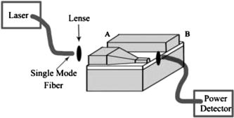
Waveguides based on silicon-on-insulator (SOI)1, 2, 3 are attractive for optical integrated circuits (OICs) because of their potential compatibility with CMOS technology. Furthermore, the large difference between the refractive indices of the core (Si) and the cladding/insulator (air and ) enables the realization of optical waveguides with submicrometer dimensions, which allows an ultrasmall bending radius.4 However, the great disparity in size between the mode field diameter (MFDs) of standard single-mode fibers and the Si waveguides will result in excessive coupling losses when they are directly coupled. Clearly, a compact and efficient mode converter is needed. Several approaches have been proposed, such as prism couplers,5 grating couplers,6 tapered optical fibers,6 and microlenses.7 The first approach needs hybrid integration between the coupler and the OIC, adding to complexity and cost. The second approach offers good efficiency but is typically narrowband. The last two approaches have good efficiency but have stringent alignment tolerances, thereby leading to high packaging costs. An ideal structure would be one that tapers in both the vertical and lateral directions8 and can be monolithically integrated with the OIC. Many techniques, such as the dip-etch process,9 dynamic etch mask technique,10 diffusion-limited etching,11 and stepped etching12 have been proposed to fabricate vertically tapered structures. All of these methods have disadvantages of either low reproducibility or labor-intensive processing. Other techniques, like dry etching using a shadow mask13, 14 requires very fine lithography and do not necessarily allow for processing on the wafer scale. In this paper, we report the fabrication and characterization of the integrated 3-D linear tapered coupler on silicon-on-insulator. The schematic diagram is shown in Fig. 1. The 3-D taper is connecting with an input and an output waveguide. The 3-D taper compresses, by field transformation, the mode field of the input waveguide (waveguide A) in the direction and simultaneously in the direction. Because the confinement of light is based on internal reflection, the slope of the taper should not be large. By selecting the suitable SOI wafers and tailoring the length of the taper, the MFDs of the input waveguide (waveguide A) and the output waveguide (waveguide B) can be well controlled for efficient coupling. Although the above description of the operation principle is made in terms of a spot-size compressor, the same structure, when it operates in reverse, can function as a spot-size expander. Clearly, the 3-D tapered coupler is simple, compact, and expected to be insensitive to a large range of the wavelength centered at . Fig. 1Schematic diagram of the 3-D taper coupling light between a single-mode fiber and planar optical devices. 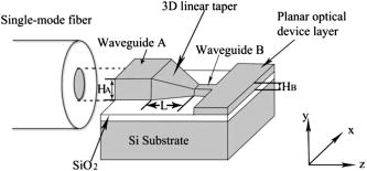 The 3-D linear taper is realized on (111) SOI wafers. It is worthy to note that the surface-orientation phase separation of commercial (111) SOI wafer is . There is slight difference, no more than , between different batches of wafers. That is, the surface is deflected from (111) crystal plane. Therefore, the vertical slope of the taper described above can be realized by anisotropic etching, because the etching rates of silicon in the ⟨100⟩ and ⟨110⟩ crystal orientations are much faster than that in the ⟨111⟩ orientation in a strongly anisotropic etchant, such as KOH.15 Figure 2 shows the scanning electronic microscopy (SEM) measurement of the profile of the top-Si layer in selected region on (111) SOI wafer after etching in KOH solution at for . The measured slope of the Si (111) crystal plane is 0.066 . The root-mean-square roughness of the (111) plane is , measured by atomic force microscope. Fig. 2SEM measurement of the profile of top-Si on Si (111)-SOI wafer after etching in KOH solution at for . 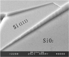 For a SMF of known MFDs to be used, the dimensions of the end facet of input waveguide (waveguide A in Fig. 1) were determined to provide desirable matching of the mode fields involved; the thickness of waveguide A was designed to be . Depending on the size of planar optical devices, the thickness of waveguide B was designed to be . In this paper, only the transmission loss was of concern. The length of the 3-D linear taper was determined to be according to the slope of (111) plane and the difference in thicknesses between waveguides A and B. In fabrication, the structure was realized by standard silicon micromachining technique. Figure 3 shows the schematic diagram of the fabrication process. A (111) SOI wafer with a -thick top Si layer was employed in the experiment. Rectangles were patterned on the top-Si layer by photolithography and dry etching techniques. Then, the wafer was bonded with another SOI wafer, whose thicknesses of the top-Si layer and buried oxide layer were and , respectively. Then, the Si substrate and buried oxide layer of initial wafer were removed. At that moment, stairs with in height were formed on the top-Si layer [refer to Fig. 3]. Thermal oxidation was then performed to engender a -thick layer as mask layer on the surface. Squares windows were patterned on the mask layer by photolithography and subsequent etching in aqueous dilute HF. After all these were done, anisotropic etching was performed in KOH solution at for to form the vertical slope. Finally, the waveguides and horizontal slopes were formed by inductively coupled plasma (ICP) etching after lithography. In the fabricated structure, the measured endface dimensions of the input and output waveguides were and , respectively. The length of the 3-D taper was , while the slope was 0.066. The SEM measurement of the fabricated structure is shown in Fig. 4. The thicknesses of the input and output waveguides can be controlled accurately by employing suitable SOI wafers. The length of the taper depends on the difference in thicknesses between input and output waveguides. Fig. 3Schematic diagram of the fabrication process: (a) patterning resist, (b)etching top-Si layer by ICP, (c) bonding to another wafer with top-Si layer, (d) removing substrate and polishing, (e) oxidation, (f) patterning, (g) etching silica in HF, (h) anisotropic etching in KOH, and (i) lithography and dry etching.  After both endfaces of the input and output waveguides were polished by chemical mechanical polishing, the total transmission loss from the input plane A to the output plane B, indicated in Fig. 5, were measured by exciting the input end using a lensed fiber with a MFD of . The same fiber was used to collect light for detection at the output end. Figure 5 shows the schematic diagram of characterization of the fabricated structure. A simultaneously fabricated waveguide without the 3-D linear taper was taken for comparison. It is to be noted that the output waveguide involved was very short in order to minimize the effect of its propagation loss on the accuracy of the transmission loss measurement. The total length of the device was . Therefore, the net transmission loss of the 3-D linear taper can be obtained by subtracting the transmission loss of the waveguide without 3-D taper from the total transmission loss of the waveguide with 3-D taper. Table 1 shows the measured results of the samples. The average net transmission loss of five samples measured in this way was at the wavelength of . Table 1Measured results of the samples. The insert transmision losses were measured between the input fiber and output fiber.
In conclusion, fabrication and characterization of a 3-D linear taper for efficient coupling between a single-mode fiber and planar photonic devices are reported. The input waveguide, in dimension of the end facet, was compressed to dimensions of in the output waveguide with average net transmission loss of at the wavelength of . The integrated 3-D taper possesses desirable features of structural simplicity, compactness, compatible with standard micromachining technics, high tolerance to fabrication errors, large optical bandwidth, and simplicity in design. AcknowledgmentThis work was financially supported by the National Science Foundation of China (Grant No. 60721004) and the Shanghai Institute of Microsystem and Information Technology Fund for Young Scholars. ReferencesW. Bogaerts, R. Baets, P. Dumon, V. Wiaux, S. Beckx, D. Taillaert, B. Luyssaert, J. Van Campenhout, P. Bienstman, and D. Van Thourhout,
“Nanophotonic waveguides in silicon-on-insulator fabricated with CMOS technology,”
J. Lightwave Technol., 23 401
–412
(2005). https://doi.org/10.1109/JLT.2004.834471 0733-8724 Google Scholar
T. Tsuchizawa, K. Yamada, H. Fukuda, T. Watanabe, J. Takahashi, M. Takahashi, T. Shoji, E. Tamechika, S. Itabashi, and H. Morita,
“Microphotonics devices based on silicon microfabrication technology,”
IEEE J. Sel. Top. Quantum Electron., 11 232
–240
(2005). https://doi.org/10.1109/JSTQE.2004.841479 1077-260X Google Scholar
V. R. Almeida, Q. Xu, C. A. Barrios, and M. Lipson,
“Guiding and confining light in void nanostructure,”
Opt. Lett., 29 1209
–1211
(2004). https://doi.org/10.1364/OL.29.001209 0146-9592 Google Scholar
D. Dai and S. He,
“Analysis for characteristics of bent rib waveguides,”
J. Opt. Soc. Am. A, 21 113
–121
(2004). https://doi.org/10.1364/JOSAA.21.000113 0740-3232 Google Scholar
A. Sure, T. Dillon, J. Murakowski, C. Lin, D. Pustai, and D. W. Prather,
“Fabrication and characterization of three-dimensional silicon tapers,”
Opt. Express, 11 3555
–3561
(2003). 1094-4087 Google Scholar
R. Hunsperger, Integrated Optics: Theory and Technology, Springer-Verlag, Berlin
(1995). Google Scholar
H. M. Presby and C. A. Edwards,
“Near 100% efficient fiber microlenses,”
Electron. Lett., 28 582
–584
(1992). https://doi.org/10.1049/el:19920367 0013-5194 Google Scholar
V. R. Almeida, R. R. Panepucci, and M. Lipson,
“Nanotaper for compact mode conversion,”
Opt. Lett., 28 1302
–1304
(2003). https://doi.org/10.1364/OL.28.001302 0146-9592 Google Scholar
T. Brenner, W. Hunziker, M. Smit, M. Bachmann, G. Guekos, and H. Melchior,
“Vertical tapers for low-loss optical fiber-waveguide coupling,”
Electron. Lett., 28 2040
–2041
(1992). https://doi.org/10.1049/el:19921307 0013-5194 Google Scholar
M. Chien, U. Koren, T. L. Koch, B. I. Miller, M. G. Young, M. Chien, and G. Raybon,
“Short cavity distributed Bragg reflector laser with an integrated tapered output waveguide,”
IEEE Photonics Technol. Lett., 3 418
–420
(1991). https://doi.org/10.1109/68.93864 1041-1135 Google Scholar
T. Brenner and H. Melchior,
“Integrated optical modeshape adapters in for efficient fiber-to-waveguide coupling,”
IEEE Photonics Technol. Lett., 5 1053
–1056
(1993). https://doi.org/10.1109/68.257189 1041-1135 Google Scholar
G. Muller, G. Wender, L. Stoll, H. Westermeier, and D. Seeberger,
“Fabrication techniques for vertically tapered spot-size transformers with very low loss,”
(1993). Google Scholar
B. Jacobs, R. Zengerle, K. Faltin, and W. Weiershausen,
“Verticaly tapered spot size transformers by a simple masking technique,”
Electron. Lett., 31 794
–796
(1995). https://doi.org/10.1049/el:19950527 0013-5194 Google Scholar
M. Frish, J. Fijol, E. E. Fike, S. A. Jacobson, P. B. Keating, W. J. Kessler, J. LeBlanc, C. Bozler, and M. Fritze,
“Coupling of single-mode fibers to planar Si waveguides using vertically tapered mode converters,”
OSA Trends in Optics and Photonics,
(2002) Google Scholar
J. B. Price,
“Anisotropic etching of silicon with ,”
Semiconductor Silicon 1973, 339
(1973) Google Scholar
|