
|
|
|
Photonic crystals (PhCs), which are periodically corrugated optical media, have received a growing interest in recent years due to their ability to tailor light properties at the wavelength scale. Most of these efforts have been devoted to photonic band-gap properties for light guiding and design of ultra-high-quality factor cavities.1, 2, 3 More recenty, attention has been paid to the strong dispersive properties of planar photonic crystals.4, 5 Collimation, superlensing, and superprism phenomena have been reported in PhCs using specific tailoring of the PhC isofrequency surfaces.5, 6 Such properties have opened opportunities to control the propagation direction and the profiles of optical beams in periodically corrugated planar optical media. In most cases, light is injected from a slab optical waveguide and impinges at the interface between this homogeneous medium and the PhC area, leading to mechanisms of light refraction through the excitation of evancescent and propagative Bloch modes in the periodic medium. Beam shaping properties can be exploited only if a significant fraction of incident light power is coupled into the PhC area, i.e., if the impedance mismatch between the two media has been carefully taken into account using some tapering strategy.7 Previous works have adressed this problem in the case of light coupling from optical strip waveguides to PhC waveguides,8, 9, 10 but only a few works have specifically adressed this problem in the case of light coupling into half-space photonic crystals. In Ref. 11, an immitance matching strategy has been proposed to minimize the reflected power at the interface with semi-infinite PhCs. Momeni and co-workers have also proposed an adiabatic matching approach for coupling of light into planar PhCs,12 while Lee and co-workers have explored a method based on anti-reflection PhC layers.13 Modifying the shapes of holes was also proposed in Ref. 14, but the technological feasiblity of etching such holes was then not considered. Moreover, all these works have adressed the problem only from a theoretical point of view. In this letter, we report experimental results showing the benefit of a gradual PhC interface to increase optical power transmission in periodically corrugated media up to the first PhC band-gap frequency of strong index contrast slab PhCs, i.e., in the slow light regime. Among the possible applications, this could serve to strengthen optical nonlinear effects in integrated optical devices. Experimental optical transmission across a nonoptimized square PhC area, i.e., with no gradual interface, is presented first. In a second step, it is compared with the same PhC region optimized with gradual stages at both input and output ends. Figure 1 shows a scanning electron microscope (SEM) view of the realized experimental device. It consists of a lattice parameter square PhC of circular airholes of normalized radius etched in a silicon-on-insulator (SOI) wafer with a -thick top silicon film separated from the Si substrate by a layer. Refractive slab waveguides were defined using a RAITH150 electron beam lithography process using negative resist. The PhC structure was separately insolated by means of a lithography process with positive resist. The photoresist patterns were transferred to the -thick top silica cladding layer using a reactive ion etching system. This layer served as a mask to etch the silicon film through a anisotropic etching process. Fig. 1(a) Large-scale SEM view of the realized PhC inserted in a slab waveguide area with -wide input and -wide output SOI strip waveguides: the output waveguide width was chosen to ensure full light collection in spite of beam divergence occuring in the slab waveguide area after the PhC region. (b) Detailed SEM view of the PhC area. 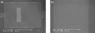 The PhC area is made of 39 rows of holes, and the input and output SOI strip waveguides have widths of and , respectively. These waveguides allow light injection and light collection, respectively, in the perpendicular direction with respect to the PhC lattice interface, i.e., in the direction. Figure 2 shows the square PhC dispersion diagram calculated using the 3-D guided-wave expansion method reported in Ref. 15 In the wavelength range of interest above , the normalized frequency is typically lower than 0.2, and a photonic band gap is visible in the direction near the first band of the square PhC. Fig. 2Dispersion diagram of an asymmetrical planar airhole SOI PhC (bottom cladding is oxide and top cladding is air) calculated using the 3-D guided-wave expansion method described in Ref. 15. Silicon, oxide, and air lines are visible. 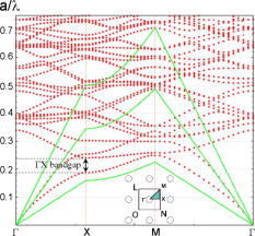 The experimental characterization was based on a setup using a tunable semiconductor laser in the spectral range between 1575 and . A linearly polarized light beam was coupled into an input waveguide with a polarization-maintaining lensed-fiber using a butt-coupling technique. The output light was collected by a objective and was measured with a large-area IR detector. The exact value of the hole diameter was obtained from the comparison of the band-gap frequency estimated using 3-D finite difference time domain (FDTD) simulations and from experimental optical transmission spectra. Figure 3 shows this comparison for the best hole diameter of . High-frequency fringes are visible in the experimental curve due to parasistic Fabry-Pérot reflections that have been hereafter filtered. Fig. 3Comparison between the 3-D FDTD calculated spectrum of the device described in Fig. 1 and the related experimental optical spectrum showing the good agreement between simulation and sample characterization for . 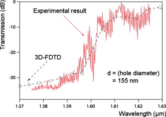 Light coupling at the edge of band 1 was further investigated by considering the possible tapering of the interface. As pointed out in Ref. 12, light reflection at the input/output interfaces near the PhC band edge is primarily due to group velocity mismatch between fast and slow waves. Here, the fast mode is related to the slab waveguide mode excited in the slab waveguide area before the light arrival at the interface with the PhC area. In order to increase the light coupling efficiency within the PhC area, 10 rows of holes were added at both input and output interfaces. From the desired PhC lattice at the center, a chirp was introduced in the direction (only) for both the lattice parameter and hole diameter, respectively. The lattice parameter in the ’th row of holes ) was taken as 98% of the previous value obtained for the ’th one. A similar chirp was introduced for the hole diameter, but with a 97% decrease rate instead of 98%. The final lattice parameter and hole diameter values were then and , respectively. Figure 4 shows the calculated light group velocity for the first band in the direction for the 10 different PhCs corresponding to the sets of lattice period and hole diameter values of the input/output tapering stages. It highlights the operation of gradual decrease of light group velocity in order to suppress the impedance mismatch between fast and slow waves at the interface between the slab waveguide and the 2-D PhC area. Fig. 4Light group velocity in the direction for 10 different PhCs. The lattice parameter and hole diameter values of these PhCs have been chosen to correspond to those of the 10 rows of holes of the input and ouput tapers of the device shown in Fig. 5. 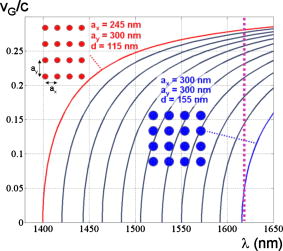 Fig. 5SEM view of the chirped PhC output interface after correction of proximity effects: 98% and 97% of lattice and hole diameter chirps, respectively, have been considered from each additional row of holes for the last 10 rows of holes. 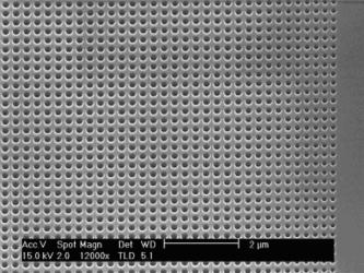 For the practical realization of the PhC device, proximity effects during e-beam lithography steps were taken into account. We realized for this a specific characterization allowing the estimation of the correct resist exposure to minimize proximity effects.16 The whole technological process allowed the fabrication of graded PhCs, i.e., fabrication tolerances did not prevent the possible use of physical effects due to lattice and hole diameter chirps. Figure 5 shows an SEM view of the realized chirped PhC. Figure 6 shows the experimental comparison between the initial PhC structure (without tapers) and the final PhC one (with tapers). It shows the benefit coming from the use of a gradual interface to efficiently inject light in the periodically corrugated optical medium. In this case, high-frequency oscillations, due to parasistic Fabry-Pérot cavities were removed from the experimental results. Fig. 6Comparison between experimental optical transmission spectra with and without the optical tapers described in the captions of Fig. 4 and Fig. 5. 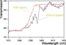 To conclude, planar PhCs have interesting properties to control light beam profiles and dispersion properties, but light has to be first efficiently injected into periodic media. We report in this paper experimental results about the possible use of a gradual interface to inject light in semi-infinite PhC areas. This approach is an efficient way to maximize light coupling into corrugated media, at least when power reflection is due to a group velocity mismatch between different regions. Such a result shows the possibility of exciting Bloch waves of planar PhCs close the photonic band-gap edge. This is interesting from a practical point of view, as most giant dispersive effects are obtained in this wavelength regime. ReferencesS. J. McNab, N. Moli, and Y. A. Vlasov,
“Ultra-low loss photonic integrated circuit with membrane-type photonic crystal waveguides,”
Opt. Express, 11
(22), 2927
–2939
(2003). 1094-4087 Google Scholar
A. Y. Petrov and M. Eich,
“Zero dispersion at small group velocities in photonic crystal waveguides,”
Appl. Phys. Lett., 85
(21), 4866
–4868
(2004). https://doi.org/10.1063/1.1815066 0003-6951 Google Scholar
Y. Akahane, T. Asano, and B.-S. Song,
“High-Q photonic nanocavity in a two-dimensional photonic crystal,”
Nature (London), 425 944
–947
(2003). https://doi.org/10.1038/nature02063 0028-0836 Google Scholar
L. Wu, M. Mazilu, J.-F. Gallet, and T. F. Krauss,
“Square lattice photonic crystal collimator,”
Photonics Nanostruct. Fundam. Appl., 1 31
–36
(2003). https://doi.org/10.1016/S1569-4410(03)00004-X 1569-4410 Google Scholar
B. Momeni, J. Huang, M. Soltani, M. Askari, S. Mohammadi, M. Rakhshandehroo, and A. Adibi,
“Compact wavelength demultiplexing using focusing negative index photonic crystal superprisms,”
Opt. Express, 14
(6), 2413
–2422
(2006). https://doi.org/10.1364/OE.14.002413 1094-4087 Google Scholar
D. Bernier, X. Le Roux, A. Lupu, D. Marris-Morini, L. Vivien, and E. Cassan,
“Compact, low cross-talk CWDM demultiplexer using photonic crystal superprism,”
Opt. Express, 16
(22), 17209
–17214
(2008). https://doi.org/10.1364/OE.16.017209 1094-4087 Google Scholar
S. G. Johnson, P. Bienstman, M. A. Skorobogatiy, M. Ibanescu, E. Lidorikis, and J. D. Joannopoulos,
“Adiabatic theorem and continuous coupled-mode theory for efficient taper transitions in photonic crystals,”
Phys. Rev. E, 66 066608
(2002). https://doi.org/10.1103/PhysRevE.66.066608 1063-651X Google Scholar
A. Mekis and J. D. Joannopoulos,
“Tapered couplers for efficient interfacing between dielectric and photonic crystal waveguides,”
J. Lightwave Technol., 19
(6), 861
–865
(2001). https://doi.org/10.1109/50.927519 0733-8724 Google Scholar
T. Baba, D. Mori, K. Inoshita, and Y. Kuroki,
“Light localizations in photonic crystal line defect waveguides,”
IEEE J. Sel. Top. Quantum Electron., 10
(3), 484
–491
(2004). https://doi.org/10.1109/JSTQE.2004.829201 1077-260X Google Scholar
R. Biswas, Z. Y. Li, and K. M. Ho,
“Impedance of photonic crystals and photonic crystal waveguides,”
Appl. Phys. Lett., 84
(8), 1254
–1256
(2004). https://doi.org/10.1063/1.1649815 0003-6951 Google Scholar
J. Ushida, M. Tokushima, M. Shirane, A. Gomyo, and H. Yamada,
“Immitance matching for multidimensional open-system photonic crystals,”
Phys. Rev. B, 68 155115
(2003). https://doi.org/10.1103/PhysRevB.68.155115 0163-1829 Google Scholar
B. Momeni and A. Adibi,
“Adiabatic matching stage for coupling of light to extended Bloch modes of photonic crystals,”
Appl. Phys. Lett., 87 171104
(2005). https://doi.org/10.1063/1.2115081 0003-6951 Google Scholar
S.-G. Lee, J.-S. Choi, J.-E. Kim, and H. Y. Park,
“Reflection minimization at two-dimensional photonic crystal interfaces,”
Opt. Express, 16
(6), 4270
–4277
(2008). https://doi.org/10.1364/OE.16.004270 1094-4087 Google Scholar
T. Baba and D. Oshaki,
“Interfaces of photonic crystals for high efficiency light transmission,”
Jpn. J. Appl. Phys., Part 1, 40 5920
–5924
(2001). https://doi.org/10.1143/JJAP.40.5920 0021-4922 Google Scholar
Guided Mode Expansion (GME) software: http://fisicavolta.unipv.it/dipartimento/ricerca/Fotonici/Index.htm Google Scholar
R. Wüest, P. Strassera, M. Jungob, F. Robina, D. Ernib, and H. Jäckela,
“An efficient proximity-effect correction method for electron-beam patterning of photonic-crystal devices,”
Microelectron. Eng., 67–68 182
–188
(2003). 0167-9317 Google Scholar
|


