|
|
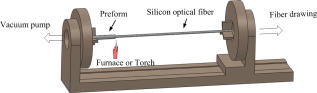
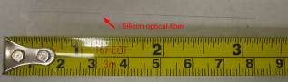
1.IntroductionOptical fibers form the basis of modern telecommunications by their extraordinary abilities of manipulating photons over a long distance. On the other hand, semiconductor-based optoelectronic devices, such as lasers, amplifiers, and detectors, are the key elements to generate, reshape, and capture photons. Conversion from photons to electrons is needed in order to demodulate the optical signal. However, conversion between optical and electronic signals not only increases the complexity of the overall system, but also seriously degrades the transmission speed and increases the total loss. Although silicon-waveguide-based optoelectronic devices have been realized, such as a Raman waveguide laser in the near-infrared (NIR) region1 and an image amplifier in the medium-wave-infrared (MWIR) region,2 it is desirable to avoid such conversions and maintain the photons within the fiber. Silicon-based all-fiber optoelectronic devices are highly desired for the future telecommunication networks. In addition, regular optical fibers are made of fused silica with some special dopants in the core, such as germanium. They cut off at a wavelength of . In comparison, silicon allows low-loss optical transmission to the MWIR region . Particularly, most chemical and biological agents have stronger and more unique signature absorptions in the MWIR region as compared to the NIR region, which can make silicon optical fibers ideal sensing devices. Silicon core optical fibers have been fabricated using high-pressure microfluidic chemical deposition technology.3 However, this technology experiences difficulties in order to fabricate fibers at a longer length and in a large quantity. Recently, silicon optical fibers have also been fabricated by the rod-in-tube technique using a traditional fiber draw tower.4 Although suitable for regular optical fiber manufacturing in a large quantity, the fiber draw tower is not suitable for fabricating small quantities of special fibers that are still in the development stage and that may require many iterations to be performed quickly to determine the proper processing parameters. Once all these parameters are determined, a fiber draw tower might then be used to make large quantities of the fiber at the predetermined conditions. In Ref. 4, fibers were drawn from a preform that had a silicon rod sleeved by silica tubes. These fibers ranged in diameter from , making them inflexible. Thus, their functionalities as practical fibers are very limited. 2.Experiment and AnalysisIn this research, silicon optical fibers are made with the powder-in-tube technique. The preform is made in such a way that high-purity silicon metal powders are placed inside the optical-purity silica tube, with an outer diameter of and an inner diameter of . Silicon optical fibers are fabricated from the preform by utilizing a custom-made fiber drawing system, as illustrated in Fig. 1. This system is specifically designed for specialty fiber drawing. The fiber drawing system has two chucks, which are used to clamp the silica preform and can spin together or separately at precisely controlled speeds. The second chuck can also be moved linearly, which draws the fiber from the preform when heated and softened by a hydrogen-oxygen torch over . The preform is clamped in one of the chucks, and another silica tube is clamped in the second chuck, which serves to support and allow mechanical force to be imparted on the molten preform. The preform is set to spin by slowly rotating the two chucks at the same rate in order to be heated uniformly. When the preform is heated by the hydrogen-oxygen flame to a temperature over , the silicon metal is melted and the silica tube is softened. Silicon optical fiber is produced by moving the second chuck along the platform, which maintains linearity. A vacuum is applied during the fabrication process in order to remove air from the preform. The vacuum is maintained as the preform is heated and during the fiber drawing. The fiber drawing system has the ability to control parameters such as the fiber diameter and the length, fiber drawing speed, etc. The fabricated silicon optical fibers have cladding diameters in the range of and core diameters in the range of and an approximate overall length of , as shown in Fig. 2. The fiber end face was also analyzed by an optical microscope and a scanning electron microscope (SEM). The optical and the SEM micrographs of the silicon optical fiber end face are shown in Fig. 3. In Fig. 3, a bright core can be seen by illuminating the fiber with a white light source. In Fig. 3, a silicon optical fiber with a cladding diameter of and a core diameter of was imaged. The silicon core and silica cladding have a clear phase difference, and the core/cladding boundary maintains uniformity over the entire fiber length. Fig. 3(a) Optical micrograph when the end face is illuminated by a white light. (b) SEM micrograph of a silicon optical fiber with a core diameter of and a cladding diameter of . The inset in the lower-left corner shows a clear phase difference between the silicon core and the silica cladding. 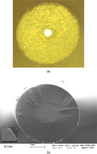 The optical transmission characteristics were also studied. In the experiment, the silicon fiber was mounted on an optical stage and axially aligned with the lead-in and the lead-out single-mode fibers, which were mounted on separate three-dimensional (3-D) stages for precision alignment. Light is delivered from the lead-in fiber into the silicon fiber through free space. The transmitted light is collected by the lead-out fiber, which transmits the signal into the spectrum analyzer. The optical transmission is measured in the wavelength range between and by a Micron Optics CTS system (Model Number SI-720). The transmission spectrum is shown in Fig. 4. The overall coupling efficiency is highly dependent on the optical alignment and is very sensitive to changes in the environmental conditions. Making an accurate numerical judgment of the transmission loss is difficult at this time. A rough estimation can be made by comparing the silicon optical fiber with a regular multimode fiber (MMF) with similar coupling conditions. The transmission spectrums of a well-cleaved MMF, a silicon optical fiber, and an uncleaved MMF are shown in Fig. 4. Fig. 4Optical transmission spectra of a well-cleaved MMF, a silicon optical fiber, and an uncleaved MMF.  In addition to the coupling conditions, the following factors are considered as main reasons for the loss from the fiber itself:
3.ConclusionIn this research, silicon optical fibers have been fabricated by the powder-in-tube technique. These are the first such small-diameter flexible fibers to be reported by the direct drawing technique. The fabricated fibers have been confirmed to have good physical and optical characteristics. These fibers can be potentially developed into optical communication and sensing devices. The powder-in-tube technique is versatile, and it can be utilized to fabricate similar devices with different dimensions and core/cladding materials, such as optical fibers with different dopants. ReferencesB. Jalali, V. Raghunathan, D. Dimitropoulos, and O. Boyraz,
“Raman-based silicon photonics,”
IEEE J. Sel. Top. Quantum Electron., 12 412
–421
(2006). https://doi.org/10.1109/JSTQE.2006.872708 1077-260X Google Scholar
V. Raghunathan, D. Borlaug, R. R. Rice, and B. Jalali,
“Demonstration of a mid-infrared silicon Raman amplifier,”
Opt. Express, 15 14355
–14362
(2007). https://doi.org/10.1364/OE.15.014355 1094-4087 Google Scholar
P. J. A. Sazio, A. Amezcua-Correa, C. E. Finlayson, J. R. Hayes, T. J. Scheidemantel, N. F. Baril, B. R. Jackson, D. J. Won, F. Zhang, E. R. Margine, V. Gopalan, V. H. Crespi, and J. V. Badding,
“Microstructured optical fibers as high-pressure microfluidic reactors,”
Science, 311 1583
–1586
(2006). https://doi.org/10.1126/science.1124281 0036-8075 Google Scholar
J. Ballato, T. Hawkins, P. Foy, R. Stolen, B. Kokuoz, M. Ellison, C. McMillen, J. Reppert, A. M. Rao, M. Daw, S. Sharma, R. Shori, O. Stafsudd, R. R. Rice, and D. R. Powers,
“Silicon optical fiber,”
Opt. Express, 16 18675
–18683
(2008). https://doi.org/10.1364/OE.16.018675 1094-4087 Google Scholar
P. Klocek, Handbook of Infrared Optical Materials, xiii, 335, 445 M. Dekker, New York
(1991). Google Scholar
|