|
|
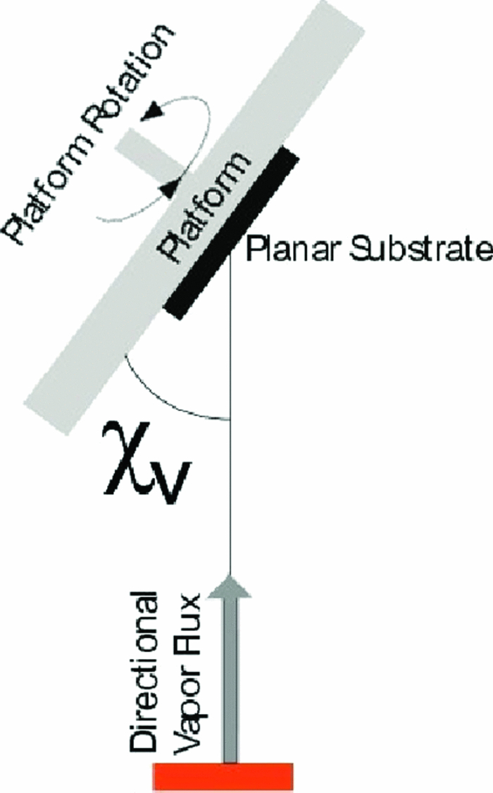
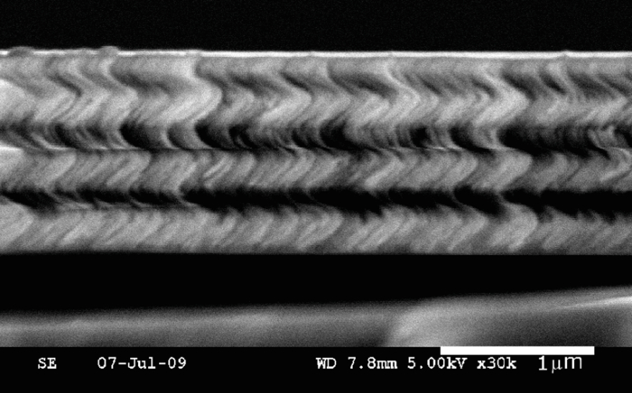
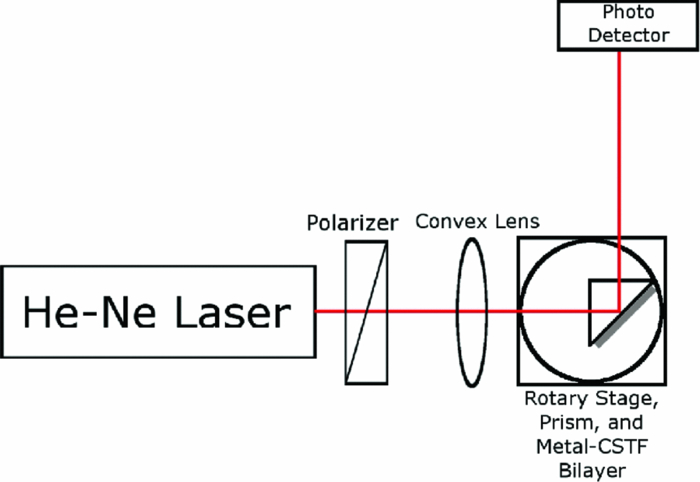
1.IntroductionSurface plasmon resonance (SPR) is the quantum oscillation of charges guided by the planar interface of a metal and dielectric material. The quantum is called a surface plasmon polariton (SPP), and resonance occurs when energy from photons in a dielectric material is transferred to collective oscillations, called plasmons, of free electrons guided by the metal/dielectric interface.1, 2, 3 SPR has been extensively studied,3, 4, 5 particularly for sensing chemical and biochemical species. Typically, SPPs are excited at noble metal/homogeneous dielectric material interfaces and can be observed only for the parallel polarization of the incident laser beam, p-polarization (the direction of the polarization lies in the plane of incidence).3 Recent theoretical studies6, 7, 8, 9 have shown that by replacing the homogeneous dielectric material by a linear, anisotropic dielectric material, more than one SPP wave can be launched, and in the same film SPP waves can also be observed for s-polarization of the incident laser beam (the direction of the polarization is perpendicular to the plane of incidence).6, 7 The theoretical basis for the excitation of multiple SPR and excitation by s-polarization is explained by Faryad and Lakhtakia.10 Although these SPP waves propagate with the same frequency, they have different phase speeds, polarization states, attenuation rates, and field distributions. Multiple SPP waves in a chiral sculptured thin film (CSTF) have been experimentally observed for p-polarized incident light.11 We report the experimental observation of multiple SPR guided by a metal and a chiral sculptured thin film (metal/CSTF) interface, providing experimental confirmation of the theoretical predictions of Motyka, Polo, and Lakhtakia.6, 7, 8, 9 2.Experimental ProcedureTo fabricate the metal/CSTF interfaces, magnesium fluoride CSTFs were deposited on borosilicate glass slides that had been previously coated with a gold film. The gold films were deposited by sputtering gold in argon plasma at 5 mTorr. Prior to sputtering, the chamber had been pumped to a base preasure of ∼10−6 Torr. Film thickness was monitored in situ by a quartz crystal monitor, and deposition was carried out until the thickness of the gold film reached ∼31 nm. Magnesium fluoride (MgF2) was then thermally evaporated at base pressures between 1- and 3-μTorr with a current of ∼125 A being passed through a 12 × 44 mm dimpled tungsten boat. The chiral morphology was produced by fixing the substrates at an oblique angle measured between the substrates' surfaces and the average direction of the vapor flux generated at the thermal source. We designate this angle as χv or the vapor flux angle, as shown schematically in Fig. 1. For all depositions, χv was fixed at 15 deg. The CSTFs were either two or three periods, each period being 400 nm in thickness. The substrates were then slowly rotated by a computer controlled stepper motor about an axis along the substrate's normal while maintaining a constant deposition rate as indicated by a quartz crystal monitor. To maintain a stable vapor flux, a low deposition rate of 0.4 nm s−1 was required. To allow for this low deposition rate and desired 400 nm pitch, the rotation about the surface normal was broken up into 20 steps of 18 deg with a 50-s pause between each successive step. This combination of deposition rate and substrate motion gave smooth helical film morphology to the MgF2 layer and a pitch of ∼400 nm. Multiple periods were produced by continuing the deposition while several rotations occurred, with approximately 17 min elapsing between each full rotation. Once the desired number of periods were deposited, the source was shuttered and the sample was allowed to cool under vacuum for an hour before being removed. Figure 2 shows a cross sectional SEM of a typical sample. Surface plasmons occur at the interface of two different materials, usually one with a positive dielectric constant and one with a negative dielectric constant. This can be achieved with a prism in optical contact with a thin metal layer. A key condition that allows for the propagation of surface plasmons is that the real part of the dielectric permittivity of the metal must be negative. This condition is met by noble metals, silver and gold for example. An important property of surface plasmons is that their k-vector is greater than that of light at the same frequency. To couple the surface plasmons, the parallel component of the incident k-vector must be greater than the free-space k-vector. A surface plasmon is excited when the beam is impinging on the interface at a well-defined angle determined by the optical parameters of the film. This is observed by a characteristic dip in the intensity of the reflected light.12, 13 The glass slide was attached with its uncoated side to a BK-7 prism with a refractive index of 1.514 for a 632.8-nm wavelength. Immersion oil (Olympus, Center Valley, Pennsylvania) of the same refractive index was used to make optical contact between the prism and the glass substrate on which the metal/CSTF interface was created. The prism with the sample was mounted on a Sigma Koki (Hidaka City, Japan) turntable, which provides a precision of 1 arc min. A polarized He-Ne laser beam (5 mW, λ = 632.8 nm) was focused onto the interface between the glass and the metal film by a lens of focal length 10 cm after passing through a linear polarizer. The power of the beam incident on the prism was 3.6 mW. The power of the reflected light was measured using a Newport (Irvine, California) photodetector as a function of the angle of incidence. A schematic diagram of the experimental setup is shown in Fig. 3. 3.Results and DiscussionA series of experiments were performed with samples of different CSTF thicknesses and a different number of periods. The results showed that in all CSTF samples, SPR are observed for both polarizations of the impinging laser beam. Figures 4 and 4 show the overall reflectance versus the angle of incidence on the metal/CSTF bilayer for two and three periods of CSTF, with s- and p- polarized incident laser beams, respectively. The results presented are for CSTFs of thicknesses ∼800 and ∼1200 nm. Multiple resonances are evident as indicated by the dips in the reflectance. These dips in the reflectance may also be caused by the waveguide modes excited in the CSTF. Since the waveguide resonances involve the bulk of the CSTF, their angular locations would depend on the thickness of the CSTF. However, there are two sharp dips in both Fig. 4 (labeled 1 at ∼45 deg and 2 at ∼63 deg) and Fig. 4 (labeled 3 at ∼50 deg and 4 at ∼57 deg) that could be considered as independent of the number of periods of CSTF, i.e., the thickness of the film. These dips indicate the launch of four different SPR, two for s-polarized incident light and two for p-polarized incident light. The experimental observation of multiple SPR therefore confirms the theoretical predictions.6, 7, 8, 9 Comments on the angular location and width of SPR dips are discussed by Polo and Lakhtakia.6 These resonant phenomenon could be used for sensing purposes such as detecting biomolecules of interest for water safety.5 Fig. 4Reflectance versus angle of incidence for (a) s-polarized and (b) p-polarized light, both with two- and three-period CSTFs. The s-polarization data show two sharp-overlapping dips at ∼45 and ∼63 deg, indicating the presence multiple SPR for s-polarized light. The p-polarization data show two sharp-overlapping dips at ∼50 and ∼57 deg, indicating the presence of multiple SPR for p-polarized light. 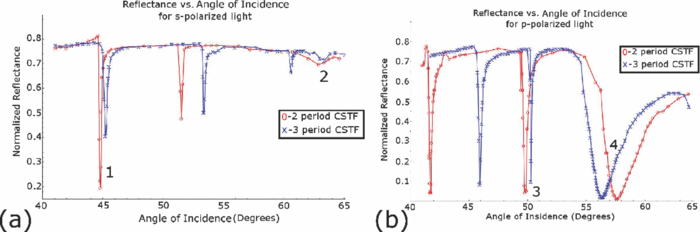 4.ConclusionOur experimental results confirm that more than one SPP wave of the same frequency but different phase speed can be supported by the planar interface of a metal and chiral sculptured thin film. Multiple SPR may have a significant impact on many sensing, imaging, and plasmon communication technologies.8, 9 AcknowledgementsThis research was done in the frame of a collaborative project between Indiana University of Pennsylvania, Penn State University, Millersville University of Pennsylvania, and Edinboro University of Pennsylvania. Collectively this group makes up the Pennsylvania Center for Advanced Nanosensing or PeCAN. ReferencesM. Dragoman and D. Dragoman,
“Plasmonics: application to nanoscale terahertz and optical devices,”
Prog. Quantu Electron., 32 1
–41
(2008). https://doi.org/10.1016/j.pquantelec.2007.11.001 Google Scholar
S. A. Maier, Plasmonics: Fundamentals and Applications, Springer, New York
(2007). Google Scholar
J. Homola, S. S. Yee, and G. Gauglitz,
“Surface plasmon resonance sensors: review,”
Sens. Actuators B, 54 3
–15
(1999). https://doi.org/10.1016/S0925-4005(98)00321-9 Google Scholar
J. Homola, Surface Plasmon Resonance Based Sensors, Springer, Heidelberg, Germany
(2007). Google Scholar
I. Abdulhalim, M. Zourob, and A. Lakhtakia,
“Surface plasmon resonance for biosensing: a mini-review,”
Electromagn., 28 214
–242
(2008). https://doi.org/10.1080/02726340801921650 Google Scholar
J. A. Polo Jr. and
A. Lakhtakia,
“On the surface plasmon polariton wave at the planar interface of a metal and a chiral sculptured thin film,”
Proc. R. Soc. A, 465 87
–107
(2009). https://doi.org/10.1098/rspa.2008.0211 Google Scholar
J. A. Polo Jr. and
A. Lakhtakia,
“Energy flux in a surface-plasmon-polariton wave bound to the planar interface of a metal and a structurally chiral material,”
J. Opt. Soc. Am. A, 26 1696
–1703
(2000). https://doi.org/10.1364/JOSAA.26.001696 Google Scholar
M. A. Motyka and A. Lakhtakia,
“Multiple trains of same-color surface plasmon-polaritons guided by the planar interface of a metal and a sculptured nematic thin film,”
J. Nanophoton., 2 021910
(2008). https://doi.org/10.1117/1.3033757 Google Scholar
M. A. Motyka and A. Lakhtakia,
“Multiple surface-plasmon-polariton waves localized to a metallic defect layer in a sculptured nematic thin film,”
J. Nanophoton., 3 033502
(2009). https://doi.org/10.1117/1.3147876 Google Scholar
M. Faryad and A. Lakhtakia,
“Surface plasmon-polariton wave propagation guided by a metal slab in a sculptured nematic thin film,”
J. Opt., 12 085102
(2010). https://doi.org/10.1088/2040-8978/12/8/085102 Google Scholar
Devender, D. P. Pulsifer, and A. Lakhtakia,
“Multiple surface plasmon polariton waves,”
Electron. Lett., 45 1137
–1138
(2009). https://doi.org/10.1049/el.2009.2049 Google Scholar
H. J. Simon, D. E. Mitchell, and J. G. Watson,
“Surface plasmons in silver films: a novel undergraduate experiment,”
Am. J. Phys., 43 630
–636
(1975). https://doi.org/10.1119/1.9764 Google Scholar
G. Hass, M. H. Francombe, and R. W. Homan, Physics of Thin Films, Advances in Research and Development, 9 Academic Press, New York
(1977). Google Scholar
|