|
|
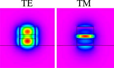
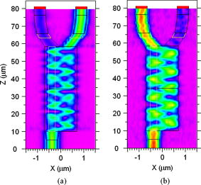
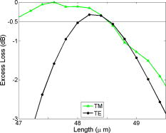
1.IntroductionThe development of photonic circuits and the emergence of electronic-photonic circuits show that integration becomes the key to the success of these photonic devices, which makes compact waveguide devices with low excess loss an essential component in integrated circuit design. One crucial problem in ultrasmall waveguide devices is the structural birefringence that is impossible to eliminate. Birefringence-induced polarization dependence is mostly undesirable because it causes phase shifts in all interferometric devices, such as Mach–Zehnder interferometers and ring resonators. In order to have polarization control, orthogonal transverse electric (TE) and transverse magnetic (TM) polarizations have to be split and processed separately. Therefore, polarization diversity circuits with polarization splitters are critical and necessary in ultrasmall device design. There are primarily two mechanisms for polarization splitters. One mechanism is waveguide-based polarization splitters, such as directional couplers,1 Mach–Zehnder scheme interferometers,2 and multimode interference splitters.3, 4 Although much research has been done in the design and fabrication of these types of polarization splitters, the majority of these approaches have limitations, such as excess loss or requiring external stress-inducing schemes. The other mechanism is the photonic crystal (PC)–based polarization splitter.5 Because of the nature of the PC, the existence of a TM photonic bandgap provides a mean for TE and TM splitting. However, the PC fabrication process is not compatible with general integrated circuit processes, which makes this approach difficult to deploy at the current stage. Polarization separation based on self-imaging devices has been studied for the lithium niobate and glass material systems.6 But the lithium niobate and glass material systems are not suitable for integration due to the bulky size and noncompatibility with standard fabrication. The nonbirefringent silicon material system is a better candidate for integration because of its matured fabrication technology, low cost, and compatibility with most of the electronic/photonic devices. A simple structure polarization splitter based on the silicon material system is proposed in this paper. A multimode interference (MMI) polarization splitter on a commercial substrate silicon-on-insulator is investigated. The simplicity of the slot waveguide structure and the compact size make the proposed splitter a great candidate for photonic integrated circuits or electronic-photonics circuits. The characteristics of the slot waveguide are explained, followed by a discussion of limited-modes MMI design for a compact-size splitter. The performance and tolerance of the device are analyzed and presented at the end. 2.Waveguide Structure and Coupler DesignThe slot waveguide core is composed of an upper silicon layer , a sandwiched silicon-oxide layer , and a lower silicon layer . The splitter schematic structure is shown in Fig. 1 and the slot waveguide cross section is depicted by the inset. The structure is analyzed by the rigorous finite difference method (mode solver) and the 3-D vector beam propagation method. The operating wavelength of the design is . Fig. 1Schematic structure of the polarization splitter. Inset shows the geometry of the MMI section and the waveguides cross section. 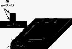 In the slot structure, the structural birefringence is large even though there is no material birefringence in the Si material system. The characteristics of TE polarization are more sensitive to the lateral structure because the major electrical field of TE is in the horizontal direction; the characteristics of TM polarization are more sensitive to the vertical structure because the major electrical field of TM is in the vertical direction. As shown in Fig. 2, the majority of the TE field is contained in the upper and lower Si layers, whereas the majority of the TM field is contained in the sandwiched layer.7 As a result, the effective indices of the TE and TM polarizations have large differences. This birefringence causes a large beat-length difference between TE and TM polarizations. As shown in Fig. 3, the beat-length difference between TE and TM polarizations changes as a function of the MMI section width (given a fixed sandwiched-layer index of 1.5, upper and lower Si-layer thicknesses of , and a sandwiched-layer thickness of ). Fig. 3TE and TM beat-length difference versus MMI width for different sandwiched layers at fixed sandwiched thickness . 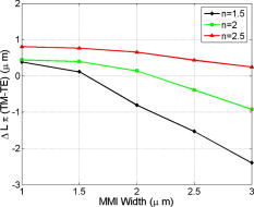 In the MMI coupler, polarization splitting is obtained if the mirrored single image position of TE polarization and the direct single image position of TM polarization are the same, or vice versa.6 The images can be expressed as8 where is the total number of guided modes supported in MMI section, is the beat length, and is the modal excitation coefficient, which can be calculated with the overlap integral. Clear single images formed at lengths of (where is an integer).8As the MMI width reduces, the number of guided modes reduces. Once the MMI section guide limited modes, such as four modes, the field can be expressed as follows, at distance : Without losing generality, can be set to 1. By inspection, the phase is not a multiple of only when . Clear self-single imaging happens when all modes experience phase shifts of a multiple of . However, the power excitation coefficient is a function of the input-field offset, the lateral distance between the center of the MMI section and the access waveguide.8 , , and show weak dependence on the input offset, but is strongly dependent on the input offset. The wide MMI is taken as an example with the input access waveguide width of and vertical structure identical to that of the MMI region. As shown in Fig. 4, the power excitation coefficient is very small when the offset is . With the input offset to the minimum excitation point, the summation of the fields at distance is almost the replica of the input-field image with the phase of the second mode being slightly off. The images at those positions are clear and have excess loss of . This holds true for both TE and TM polarizations. Fig. 4The power excitation coefficients of the MMI with the wide access waveguide; the sandwiched layer index is 1.5. 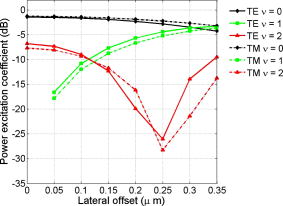 The beat length difference between TE and TM polarizations is large due to the structure-induced birefringence. The TE and TM polarizations can be routed to different outputs in minimum length,6 if the MMI length is designed to satisfy the following condition (where and are integers): An example is demonstrated and analyzed here. The vertical structure is as previously stated. The MMI width is chosen as to ensure easy separation between the two output ports but support only four modes for TE polarization and three modes for TM polarization. The single-mode access waveguides and taper are adopted. The offset between input waveguide and MMI center is adjusted to due to the existence of the taper. The first mirrored-image position of TE and TM polarizations can be found at 11.32 and , respectively, according to the BPM results. Referring to Eq. 3, when and , the TE and TM polarizations form clear single images at cross and through ports, respectively. The MMI length is adjusted to mainly due to the phase errors from the approximations of the self-image principle;7 it is also the effect of the input and output tapers. Excellent splitting between TE and TM polarizations is demonstrated in Fig. 5. The TE polarization is routed to the cross output, while the TM polarization is routed to the through output. The extinction ratios are 12.7 and for the TE and TM ports, respectively. The excess losses are 0.3 and for TE and TM, respectively. For throughput, the MMI section length error tolerance is as shown in Fig. 6, and the width error tolerance and wavelength error tolerances are 8 and , respectively. The extinction ratios for TE and TM modes are higher than other similar devices with comparable size and are comparable to other similar devices with much large size. This shows that the slot waveguide structure is a great candidate as a Si waveguide polarization splitter for a polarization diversity scheme. The device can be used as a polarization combiner as well. With an automated and matured Si processing technology, the proposed devices are feasible and promising. 3.ConclusionIn conclusion, this work reports a slot waveguide structure polarization splitter based on a self-imaging scheme. A slot waveguide structure is adopted to obtain a large beat-length difference between TE and TM polarizations. A limited-modes MMI section together with weak excitation of the second-order mode gives clear single images. With careful design of MMI size and input access waveguide offset, excellent splitting is demonstrated with a polarization extinction ratio of and low excess loss of for both polarizations. Relatively relaxed tolerances are also obtained. This compact polarization splitter is a promising candidate for electronic-photonic integrated circuits. ReferencesI. Liyat, A. Aydinli, and N. Dagli,
“A compact silicon-on-insulator polarization splitter,”
IEEE Photonics Technol. Lett., 17
(1), 100
–102
(2005). https://doi.org/10.1109/LPT.2004.838133 1041-1135 Google Scholar
L. B. Soldano, A. H. de Vreede, M. K. Smit, B. H. Verbeek, E. G. Metaal, and F. H. Groen,
“Mach-Zehnder interferometer polarization splitter in InGaAsP-InP,”
IEEE Photonics Technol. Lett., 6 402
–405
(1994). https://doi.org/10.1109/68.275500 1041-1135 Google Scholar
J. M. Hong, H. H. Ryu, S. R. Part, and J. W. Jeong,
“Design and fabrication of a significantly shortened multimode interference coupler for polarization splitter application,”
IEEE Photonics Technol. Lett., 15
(1), 72
–74
(2003). https://doi.org/10.1109/LPT.2002.805803 1041-1135 Google Scholar
D. M. Mackie and A. W. Lee,
“Slotted multimode-interference devices,”
Appl. Opt., 43
(36), 6609
–6619
(2004). https://doi.org/10.1364/AO.43.006609 0003-6935 Google Scholar
E. Schonbrum, Q. Wu, W. Park, T. Yamashita, and C. J. Summers,
“Polarization beam splitter based on a photonic crystal heterstructure,”
Opt. Lett., 31
(21), 3104
–3106
(2006). https://doi.org/10.1364/OL.31.003104 0146-9592 Google Scholar
D. M. Mackie, T. J. Tayag and T. E. Batchman,
“Polarization separation/combination based on self-imaging,”
Opt. Eng., 40
(10), 2265
–2272
(2001). https://doi.org/10.1117/1.1402623 0091-3286 Google Scholar
T. Fujisawa and M. Koshiba,
“Theoretical investigation of ultrasmall polarization insensitive multimode interference waveguides based on sandwiched structures,”
IEEE Photonics Technol. Lett., 18
(11), 1246
–1248
(2006). https://doi.org/10.1109/LPT.2006.875058 1041-1135 Google Scholar
L. B. Soldano and E. C. M. Pennings,
“Optical multi-mode interference devices based on self-imaging: principles and applications,”
J. Lightwave Technol., 13
(4), 615
–627
(1995). https://doi.org/10.1109/50.372474 0733-8724 Google Scholar
|