|
|
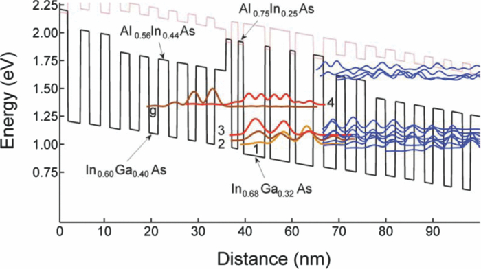
1.IntroductionThe device core of a conventional quantum cascade laser1 (QCL) is composed of a superlattice of quantum wells (QWs) and barriers of fixed alloy compositions. As a consequence, state-of-the-art devices optimized for high continuous-wave (cw) power and emitting in the 4.5- to 5.0-μm range2, 3 suffer from substantial thermally activated electron leakage from the upper laser level to the continuum. This leakage is evidenced by high sensitivity of their electro-optical characteristics to heatsink temperature variations at and above room temperature (RT)(i.e., above 300 K). That is, the characteristic temperature coefficient T0 for the threshold-current density Jth [defined by Jth(Tref+ΔT) = Jth(Tref) exp (ΔT/T0), where Tref+ΔT is the heatsink temperature and Tref is the reference heatsink temperature (e.g., 300 K)] is found to have low values of ≈140 K for 4.6-μm-emitting devices.2, 3 Similarly, the characteristic temperature coefficient T1 for the differential quantum efficiency ηd, defined by ηd(Tref+ΔT) = ηd(Tref) exp (–ΔT/T1), is also found to have a low value ≈140 K for 4.6-μm-emitting devices.2 These low values for both T0 and T1 are indirectly attributable to the small energy differential, δE = 150 to 250 meV, between the upper laser level and the top of the exit barrier.3, 4 In turn, the maximum wallplug efficiency ηwp,max in cw operation at RT, for light emitted from the front facet of devices with high-reflectivity-coated back facets, has typical values5, 6 of ≈12%, far short of theoretically predicted limits7 of ≈28% at λ ≈ 4.6 μm. In contrast, at cryogenic temperatures (40 to 80 K), where thermally activated electron leakage is negligible, maximum pulsed wallplug efficiency values as high as 50% have been achieved,8, 9 in close agreement with the theoretically predicted upper limit10 of ≈60% at λ ≈ 4.6 μm and 80-K heatsink temperature. By taking advantage of the flexibility of the metal-organic chemical vapor deposition (MOCVD) method to easily grow epitaxial QWs and barrier layers of multiple compositions in the QCL core region, we have implemented the deep-well (DW) concept11 in InP-based devices12, 13 and thus obtained δE values as high as 450 meV.12 In turn, electron leakage in and out of the active regions is substantially suppressed, which results in QCLs whose electro-optical characteristics are much less sensitive to temperature12, 13 than those for conventional devices. After deriving equations for Jth and ηd that take into account both leakage and backfilling currents, we discuss the DW concept, key results from DW QCLs, and the effects of tapering the conduction-band edge for the extractor and injection regions on the DW QCL's performance. We then show that by using the modified Jth and ηd equations, in conjunction with a model for electron thermal excitation in and out of the active region, one can obtain good agreement between calculated and experimental values for T0 in both conventional and DW-type QCLs. For optimized DW QCLs, front-facet, 300-K cw ηwp,max values >20% are projected. 2.Modified Equations for the Threshold Current and the Differential Quantum EfficiencyFigure 1 schematically shows the primary leakage paths in and out of the active region of a QCL of the double-phonon-resonance (DPR) design. Following the injection of electrons into the upper laser level (i.e., state 4), some are thermally excited to the active region's (AR’s) next-higher energy level (state 5), wherefrom they either relax to the lower-energy AR states (i.e., states 3, 2, and 1) or are further excited to the next-higher level (i.e., state 6). For state 6, electron leakage consists of both relaxation to the states 3, 2, and 1 and excitation to the upper-Γ-miniband states and subsequently to the continuum. While other parallel leakage paths exist, their currents should be negligible. On the one hand, at threshold the tunneling-injection efficiencies are close to unity, and the QW/barrier structures (e.g., In0.67Ga0.33As/Al0.64In0.36As) of conventional, high-performance 4.5- to 5.0-μm-emitting devices substantially prevent electron injection into the upper AR levels.4 On the other hand, thermal excitation from state 4 to state 6 and from state 5 to the upper-Γ-miniband states and relaxation from state 6 to the lower-Γ-miniband states are negligible because of relatively large energy differences and/or poor wave-function overlap. Fig. 1Schematic representation of the primary leakage paths for electrons injected into the upper laser level of a 4.5- to 5.5-μm-emitting QCL of the DPR design. Here g is the injector-region ground state, 1 through 6 are energy states in the active region, and the area marked as upper Γ miniband corresponds to the energy states in the upper Γ miniband of the extractor region. 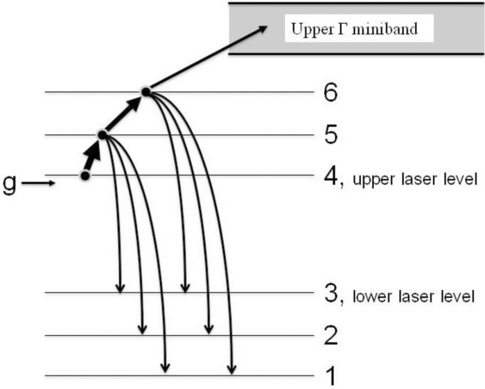 The conventional equations1 for the threshold and differential quantum efficiency should be modified to include the effects of electron leakage and, since the electrons in the injector are found to be hot,14 for electron backfilling as well. We assume that the efficiency of tunneling injection from the injector to the upper laser level1 (ηinj) is unity. The threshold-current density is then the sum of Jth in the absence of backfilling and electron leakage (J0,th) and the current densities required at threshold to compensate for backfilling (Jbf,th) and electron leakage (Jleak,th), each of which is defined below: Eq. 1[TeX:] \documentclass[12pt]{minimal}\begin{document}\begin{equation} J_{0,{\rm th}} = \frac{q}{{\tau _{{\rm up}} }}\frac{{\alpha _{{\rm tot}} }}{{g_c N_p }}, \end{equation}\end{document}Eq. 2[TeX:] \documentclass[12pt]{minimal}\begin{document}\begin{eqnarray} J_{{\rm bf,th}} &=& \frac{q}{\tau _{\rm up} }\left[ n_{s} \,\exp \left(- {\frac{\Delta _{\rm inj} + \hbar \omega_{\rm LO} [(T_{\rm eg}/T)-1]}{kT_{\rm eg}}} \right)\right.\nonumber\\ &&+\left. \left(\frac{n_{5}}{\tau_{53}}+ \frac{n_{6}}{\tau _{63}} \right) \tau_{3} \right], \end{eqnarray}\end{document}Eq. 3[TeX:] \documentclass[12pt]{minimal}\begin{document}\begin{equation} J_{{\rm leak},{\rm th}} = \frac{q}{{\tau _{5,{\rm leak}} }}n_5 + \frac{q}{{\tau _{6,{\rm leak}} }}n_6, \end{equation}\end{document}
[TeX:]
\documentclass[12pt]{minimal}\begin{document}\begin{equation*}
J \equiv J_0 + J_{{\rm bf}} + J_{{\rm leak}},
\end{equation*}\end{document}
where
Eq. 4[TeX:] \documentclass[12pt]{minimal}\begin{document}\begin{equation} J_0 + J_{{\rm bf}} \equiv \frac{q}{{\tau _4 }}n_4 \end{equation}\end{document}Eq. 5[TeX:] \documentclass[12pt]{minimal}\begin{document}\begin{equation} J_{{\rm leak}} \equiv \frac{q}{{\tau _{5,{\rm leak}} }}n_5 + \frac{q}{{\tau _{6,{\rm leak}} }}n_6 \end{equation}\end{document}A steady-state rate equation for the lower laser level (state 3) can be written as Eq. 6[TeX:] \documentclass[12pt]{minimal}\begin{document}\begin{equation} \frac{{n_3 }}{{\tau _3 }} = \left ({\frac{{n_5 }}{{\tau _{53} }} + \frac{{n_6 }}{{\tau _{63} }} + \frac{{n_4 }}{{\tau _{43} }}} \right) + \left ({\frac{{n_2 }}{{\tau _{23} }} + \frac{{n_1 }}{{\tau _{13} }}} \right), \end{equation}\end{document}Substituting Eq. 4 into Eq. 6, we get
[TeX:]
\documentclass[12pt]{minimal}\begin{document}\begin{eqnarray*}
\Delta n_{43} \equiv n_4 - n_3 &=& \frac{{J_0 + J_{{\rm bf}} }}{q}\tau _4 \left ({1 - \frac{{\tau _3 }}{{\tau _{43} }}} \right) \nonumber\\
&&- \left ({\frac{{n_2 }}{{\tau _{23} }} + \frac{{n_1 }}{{\tau _{13} }}} \right)\tau _3 - \left ({\frac{{n_5 }}{{\tau _{53} }} + \frac{{n_6 }}{{\tau _{63} }}} \right)\tau _3,
\end{eqnarray*}\end{document}
which, by using the τup definition, can be rewritten as
Eq. 7[TeX:] \documentclass[12pt]{minimal}\begin{document}\begin{eqnarray} J_0 + J_{{\rm bf}} &=& \frac{q}{{\tau _{{\rm up}} }}\left[ \Delta n_{43} + \left ({\frac{{n_2 }}{{\tau _{23} }} + \frac{{n_1 }}{{\tau _{13} }}} \right)\right.\tau _3 \nonumber\\ &&+ \left.\left ({\frac{{n_5 }}{{\tau _{53} }} + \frac{{n_6 }}{{\tau _{63} }}} \right)\tau _3 \right].\end{eqnarray}\end{document}Eq. 8[TeX:] \documentclass[12pt]{minimal}\begin{document}\begin{equation} J_0 = \frac{q}{{\tau _{{\rm up}} }}\Delta n_{43}, \end{equation}\end{document}Eq. 9[TeX:] \documentclass[12pt]{minimal}\begin{document}\begin{equation} J_{{\rm bf}} = \frac{q}{{\tau _{{\rm up}} }}\left[ {\left ({\frac{{n_2 }}{{\tau _{23} }} + \frac{{n_1 }}{{\tau _{13} }}} \right)\tau _3 + \left ({\frac{{n_5 }}{{\tau _{53} }} + \frac{{n_6 }}{{\tau _{63} }}} \right)\tau _3 } \right], \end{equation}\end{document}The backfilling expression in Eq. 9 can be further simplified if we make the following assumptions: (a) states 1 and 2 are strongly coupled to the injector miniband, so that the miniband states and states 1 and 2 are in thermal equilibrium, all sharing a common electronic temperature Teg,14 and (b) the backfilling of the lower laser level from states 1 and 2 occurs primarily via LO-phonon absorption, just like the thermal excitation from the upper laser level to the upper AR states [Eq. 16, Sec. 5]. Then we can write Eq. 10[TeX:] \documentclass[12pt]{minimal}\begin{document}\begin{eqnarray} n_2 &\approx& n_s \,\exp \,\left ({ - \frac{{\Delta _{{\rm inj}} - E_{32} }}{{kT_{{\rm eg}} }}} \right),\nonumber\\ n_1 &\approx& n_s \,\exp \,\left ({ - \frac{{\Delta _{{\rm inj}} - E_{31} }}{{kT_{{\rm eg}} }}} \right), \nonumber\\ \tau _{23} &\approx& \tau _{32}\, \exp \left ({\frac{{E_{32} - \hbar \omega _{{\rm LO}} }}{{kT_{{\rm eg}} }}} \right)\left ({\frac{{1 + n_{{\rm LO}} }}{{n_{{\rm LO}} }}} \right),\nonumber\\ \tau _{13} &\approx& \tau _{31}\, \exp \left ({\frac{{E_{31} - \hbar \omega _{{\rm LO}} }}{{kT_{{\rm eg}} }}} \right)\left ({\frac{{1 + n_{{\rm LO}} }}{{n_{{\rm LO}} }}} \right), \end{eqnarray}\end{document}For the external differential quantum efficiency ηd, by using the rate equations for a four-level system that includes electron leakage, and by defining a differential pumping efficiency at threshold, ηp = (J0, th + Jbf, th)/(J0, th + Jbf, th + Jleak, th), we obtain Eq. 11[TeX:] \documentclass[12pt]{minimal}\begin{document}\begin{equation} \eta _{\rm d} = \eta _{\rm p} \eta _{{\rm tr}} \frac{{\alpha _{\rm m} }}{{\alpha _{\rm m} + \alpha _{\rm w} }}N_p = \eta _{\rm i} \frac{{\alpha _{\rm m} }}{{\alpha _{\rm m} + \alpha _{\rm w} }}N_p, \end{equation}\end{document}Since ηtr is virtually temperature-independent, the temperature dependence of ηd is dictated by the temperature variation of both ηp and αw. These account for the experimentally observed drop in ηd with increasing temperature, especially above 300 K (i.e., the parameter T1). We also note that for a given heatsink temperature, changing the mirror loss αm by varying the cavity length L or front-facet reflectivity Rf will alter the differential internal efficiency value, since the quantity J0,th in the expression for ηp includes αm. The fact that ηi depends on L and Rf implies, in turn, that a conventional cavity-length16 or reflectivity17 study to derive ηi and αw from plots of 1/ηd versus L or 1/ηd versus 1/αm, with L or Rf varied over wide ranges, is likely to provide incorrect results for both ηi and αw. Furthermore, since αw clearly appears to increase with temperature, as deduced in Sec. 5, it may also increase with increasing αm. That is, at and above room temperature the correct value for αw has to be determined by a different method than those conventional used, which are useful only at cryogenic temperatures. 3.The Deep-Well ConceptWe initially grew a strain-compensated InP-based, 5.4-μm QCL structure of published design,18 from which we obtained19 RT lasing results comparable to the best results reported from 5.3-μm devices of same injector-doping level (2×1017 cm–3). Since the optimal growth temperature range for MOCVD (630 to 660°C) is much higher than for either gas-source molecular beam epitaxy (MBE) or MBE (500 to 530°C), it has been difficult to use MOCVD to grow the highly strained structures required for lasing below 5 μm. Therefore we designed a structure, based on deep QWs in the active region, to lase at ≈4.7 μm though grown at the same temperature (630°C) used to obtain RT lasing at 5.4 μm. Basically, only the QWs in the active region are deep, as required for4.7-μm emission (Fig. 2). Then, for strain compensation, the Al content in the barriers in and around the AR is increased from 56% to 75%, which provides much taller barriers than in conventional 4.6- to 4.8-μm QCLs.2, 3, 4, 5, 6 Another modification from conventional QCL structures is that the extractor region (i.e., the region just beyond the exit barrier) has a tapered conduction-band edge (CBE)12 that further helps to suppress electron leakage. This occurs because the wave functions corresponding to low-energy states in the upper miniband are pushed away from the AR, so that they have negligible overlap with the wave function for the upper energy state 6. The tapered-CBE extractor region is composed of an In0.66Ga0.34As well, an Al0.65In0.35As barrier, an In0.64Ga0.36As well, and an Al0.65In0.35As barrier. We further suppress electron leakage by also tapering the CBE of the injector region.13 The effects of tapering the CBE (in both the extractor and the injector regions) on electron leakage are made clear in the next section. Advantages of the DW-type 4.8-μm QCL over conventional 4.6- to 4.8-μm structures2, 3 include: (1) much greater design flexibility, since highly strained layers are limited to the active region; (2) much less carrier leakage from the active QWs, since the barrier layers in and around the AR are taller (e.g., the δE value is 200 to 300 meV larger than in conventional devices). That in turn leads to much higher T0 and T1, and potentially superior cw performance. Furthermore, ARs that suppress electron leakage are quite relevant to the development of highly efficient intersubband quantum box (IQB) lasers,20 since a longer upper-laser-level lifetime will make the devices much more sensitive to electron leakage. Thus, DW-QCL development is being pursued not only to improve the device performance and reliability, but also as a means for fulfilling the promise of IQB devices for achieving cw wallplug efficiencies as high as 50% at room temperature.21 4.Device Structures and ResultsFigure 3 compares the band diagrams and relevant wave functions of a conventional QCL3 with those for an optimized DW QCL,13 both being of the DPR design for depopulation of the lower laser level. We see first that increasing the barrier heights increases the energy difference E54 between the upper laser level (state 4) and the next-highest AR energy level (state 5), from 46 meV to 60 meV. It is shown below that this significantly reduces the carrier leakage associated with thermal excitation to state 5, followed by relaxation to the lower AR states 3, 2, and 1. For high-performance QCLs with the lower lasing level depopulated via the nonresonant extraction (NRE) design,2 E54 values as high as 63 meV have been reported.6 However, the energy difference E65 between states 5 and 6 is only about 40 meV in such devices,4 as compared to ≥80 meV for the DPR-design QCLs in Fig. 3. A lower E65 in turn leads to easy carrier escape to the continuum, as attested by the observation of relatively small values for both T0 and T1.(≈140 K).2 Fig. 3Conduction-band profile and key wave functions for: (a) conventional QCL3 emitting at 4.6 μm, (b) deep-well QCL13 emitting at λ = 4.8 μm. The upper laser level is labeled 4, while 5, 6, and 7 are higher energy states in the active region. The band profile at the top of each figure corresponds to the X valley. 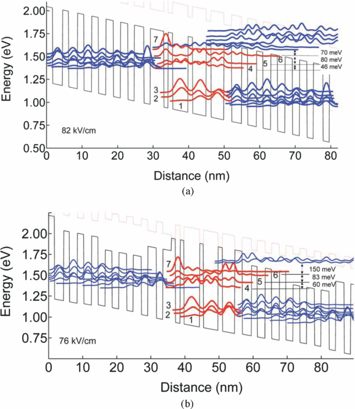 A second major difference is that the energy separation between state 6 and the bottom state of the upper Γ miniband in the extractor region, Eum,6, increases from 70 meV to 150 meV. This large enhancement occurs mostly because tapering the injector region causes the lowest state of the upper miniband to be drawn away from the extractor region, as seen in Fig. 4. As a consequence, electron leakage to the continuum, via thermal excitation from state 6 to the states of the upper Γ miniband, is completely suppressed. Fig. 4Conduction-band profile and key wave functions for deep-well QCLs with: (a) no conduction band edge (CBE) tapering; (b) tapered CBE in the extractor; (c) tapered CBE in both extractor and injector. 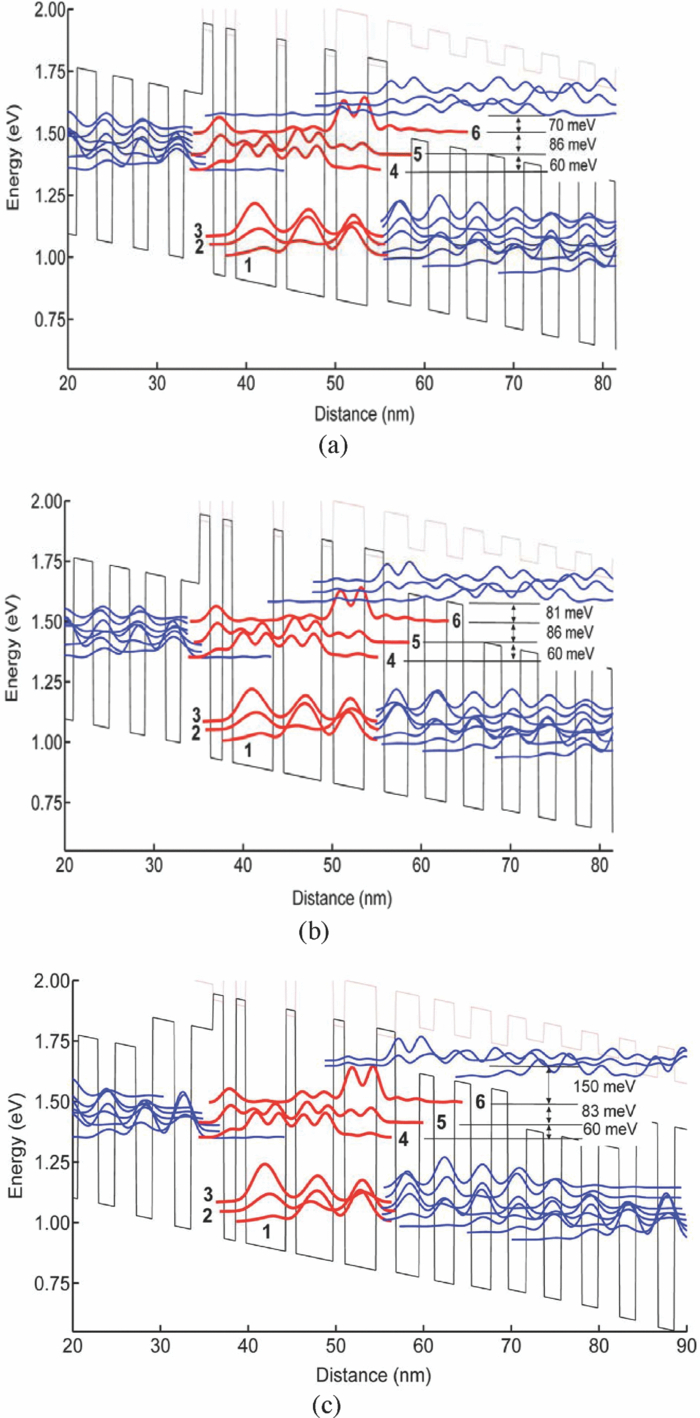 We also note that while for conventional QCLs state 7 is strongly coupled to states in the upper miniband and thus becomes a conduit for leakage to the continuum, for DW QCLs state 7 has poor overlap with upper-miniband states and thus plays no role in electron leakage. In order to clarify how tapering the injector- and extractor-region conduction-band edges affects electron leakage, Fig. 4 illustrates three cases: (a) DW structure with no CBE tapering, (b) DW structure with tapered CBE extractor, and (c) DW structure with tapered CBE for both the extractor and the injector. For fairness, the structures of cases (a) and (b) were designed to have the same emission wavelength (λ = 4.63 μm) and E54 value (60 meV) as for the published design of structure (c) in Ref. 13. Furthermore, the J0, th figure of merit (z43)2τup, where z43 is the dipole matrix element of the radiative transition, is found to have basically the same value in all three structures (≈2.5 nm2 ps). In case (a) with no CBE tapering, E65 remains basically the same (≈85 meV) as in (b) and (c), while Eum,6 has a significantly smaller value than in (c)(70 versus 150 meV), which is comparable to that for conventional DPR-design QCLs [Fig. 3]. That is, the deep wells by themselves bring about a significant increase in E54 compared to the conventional QCL (from 46 to 60 meV), which has a primary influence on electron leakage. Tapering the extractor-region CBE causes Eum,6 to increase from 70 meV to 81 meV, besides decreasing the wave-function overlap between state 6 and the upper-miniband bottom state, um1. The latter occurs because the intermediate-height barriers introduced in the extractor region push the um1 wave function away from the AR. Both effects act to significantly reduce electron leakage via scattering from state 6 to the upper miniband. More specifically, the scattering time from state 6 to the upper miniband, τ6,um, as calculated using Eq. 16 in Sec. 5, increases from 9.4 ps in the case of no CBE tapering [Fig. 4] to 33 ps in the case of tapered CBE in the extractor [Fig. 4]. Finally, from Fig. 4 it is clear that tapering the injection-region CBE causes the um1 wave function to be drawn away from the extractor region, which in turn dramatically increases Eum,6 (from 81 meV to 150 meV). The result is that electron leakage to the upper miniband is de facto shut off, as the calculated τ6,um reaches values of ≈500 ps. The electro-optical characteristics for the DW QCLs whose conduction-band diagram is displayed in Fig. 3 are shown in Fig. 5. The details of the laser structure are provided in Ref. 13, and details of the crystal growth are provided in Ref. 22. Fig. 5Deep-well QCLs 13: (a) Pulsed L-I curves as the heatsink temperature Th varies. Inset: spectrum. (b) Plots of Jth and the slope efficiency ηs as functions of Th. Here T0 and T1 are characteristic temperatures for Jth and ηs. 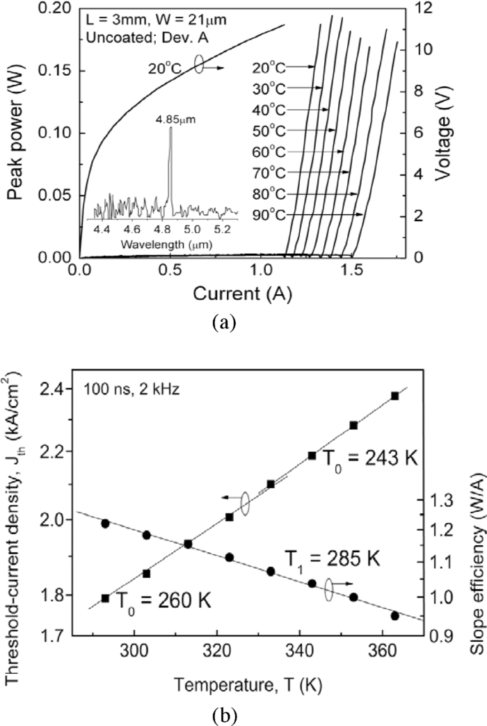 Ridge-waveguide devices were mounted episide up on Cu blocks and measured in pulsed mode (100 ns, 2 kHz). The value of Jth at 20°C is 1.78 kA/cm2, at a threshold voltage of 11.2 V, which is comparable to that for conventional devices. The characteristic temperature T0 is 260 and 243 K over the 20 to 60°C and 60 to 90°C heatsink temperature ranges, respectively. Another device with somewhat higher Jth (1.87 kA/cm2 at 20°C) exhibited T0 = 278 K over the entire 20 to 90°C temperature range.13 By comparison, T0 for a high-performance conventional 4.6-μm QC laser3 is only 143 K over the same temperature range. Both deep-well devices displayed a characteristic temperature for slope efficiency, T1, of 285 K over the 20 to 90°C range [Fig. 5], as compared to only ≈140 K for 4.6- to 4.8-μm QCLs operating over the 20 to 60°C (Ref. 2) and 0 to 50°C (Ref. 23) temperature ranges. While T0 ≈ 200 K has been observed for devices with low-doped injectors [ns = (0.5 to 0.7)×1011 cm–2],4, 24, 25, 26 most likely due to reduced carrier backfilling, such designs are not conducive to high cw powers, since the maximum current density27 Jmax scales with doping level,27 and the series resistance is high. The high T0 (260 to 278 K) and T1 (285 K) values for the deep-well QCLs not only indicate a strong suppression of carrier leakage, but also provide indirect proof that leakage to the indirect valleys (X and/or L) is not a problem in the 4.5 to 5.0-μm range when heavily strained (≈1%) In0.68Ga0.32As QWs are used. This confirms a recent report28 that the X and L minima lie farther above the Γ valley than was previously expected. Furthermore, high T0 and T1 are beneficial for cw operation. For example, the cw power, Pcw, is Eq. 12[TeX:] \documentclass[12pt]{minimal}\begin{document}\begin{eqnarray} P_{{\rm cw}} &=& A\eta _{{\rm d},{\rm cw}}(J - J_{{\rm th},{\rm cw}})\nonumber\\ &=& A\left[ {\eta _{\rm d} \,\exp \left ({ - \frac{{\Delta T_{{\rm act}} }}{{T_1 }}} \right)} \right]\left[ {J - J_{{\rm th}} \,\exp \left ({\frac{{\Delta T_{{\rm act}} }}{{T_0 }}} \right)} \right],\nonumber\\ \end{eqnarray}\end{document}Eq. 13[TeX:] \documentclass[12pt]{minimal}\begin{document}\begin{eqnarray} \Delta T_{{\rm act}} &=& T_{{\rm core}} - T_{\rm h} = R_{{\rm th}}(AJV - P_{{\rm cw}})\nonumber\\ &=& R_{{\rm th}} P_{{\rm cw}} [(1/\eta _{{\rm wp}}) - 1], \end{eqnarray}\end{document}5.Estimates for Temperature Dependence of Threshold Current and Differential Quantum EfficiencyWe use Eqs. 1 to 3, 11 to estimate the temperature variations of Jth and ηd over the range 300 to 360 K. To estimate the leakage current at threshold, we calculate the electron sheet densities in states 5 and 6 using the following relations: Eq. 14[TeX:] \documentclass[12pt]{minimal}\begin{document}\begin{equation} n_5 = n_{\rm 4,th} \frac{{\tau _{5,{\rm tot}} }}{{\tau _{45} }} + n_6 \frac{{\tau _{5,{\rm tot}} }}{{\tau _{65} }}, \end{equation}\end{document}Eq. 15[TeX:] \documentclass[12pt]{minimal}\begin{document}\begin{equation} n_6 = n_5 \frac{{\tau _{6,{\rm tot}} }}{{\tau _{56} }}, \end{equation}\end{document}Eq. 16[TeX:] \documentclass[12pt]{minimal}\begin{document}\begin{equation} \frac{1}{{\tau _{ij} }} \approx \frac{1}{{\tau _{ji} }}\,\exp \left ({ - \frac{{E_{ji} + \hbar \omega _{{\rm LO}} [(T_{\rm ei}/T)-1]}}{{kT_{{\rm ei}} }}} \right), \end{equation}\end{document}Table 1 shows calculated values for the ratio Jleak/Jth at heatsink temperatures of 300 and 360 K, and for T0, in conventional QCLs3 and DW QCLs13 of DPR design, with 4.6- to 4.8-μm wavelength, 30 periods, 3-mm-long cavity, and uncoated facets. For conventional QCLs of such parameters the Jth value at 300 K is taken to be 1.85 kA/cm2. The value was derived from experimental data3, 5 and by using our estimates of the quantity J0,th+Jbf,th for those structures with the preceding assumptions on Te5 and Te6, which provide a differential internal efficiency ηi of 70%. For DW QCLs the Jth value at 300 K for uncoated, 3-mm-long chips is 1.83 kA/cm2.13 Starting with the expression for J0,th+Jbf,th (i.e., n4,th/τ4), we add to it the expression for Jleak,th [Eqs. 3, 14, 15] and then factor out n4,th to find its value for a given Jth. Subsequently, Jleak,th was calculated at 300 K. Then, the ratio of the value of J0,th+Jbf,th at 360 K to its value at 300 K was used as a scaling factor for n4,th when calculating Jleak,th at 360 K. Table 1Measured and calculated parameters for conventional3 and deep-well13 QCLs of the DPR design (λ = 4.6 to 4.8 μm). Here Jleak/Jth is the relative electron leakage, where Jth is the threshold current density.
The primary electron leakage path is found to be relaxation from state 5 to the lower AR states (i.e., states 3, 2, and 1) of electrons thermally excited from the upper laser level (state 4) to state 5. A secondary leakage path, which is significant only for conventional QCLs, is thermal excitation from state 6 to the upper-Γ-miniband states, and subsequently to the continuum, of electrons (thermally) excited to state 6 from state 5. The relative carrier leakage (Jleak,th/Jth) is significantly smaller for DW than for conventional devices, primarily because E54 is 60 meV in the former and 46 meV in the latter. The higher E54 value, which is a consequence of the much taller barriers, affects Jleak, th mostly through the scattering time τ45. For example, the calculated values for τ45 at 360 K are 0.84 and 0.32 ps for DW-type and conventional devices, respectively. The difference is due to the E54 dependence in the thermal-activation term of Eq. 16, and also the larger τ54 value (0.21 versus 0.12 ps), which is related to the magnitude of E54 compared to the phonon energy (i.e., how nonresonant is the phonon-assisted scattering). Leakage from state 6 to the continuum is basically nonexistent in DW-type devices because of the large energy difference between state 6 and the bottom of the upper Γ miniband, Eum,6 (i.e., 150 meV), as seen from Fig. 3, which in turn gives τ6,um values of the order of 500 ps at 300 K and 200 ps at 360 K. In sharp contrast, Eum,6 in conventional devices is ≈70 meV [Fig. 3], which, coupled with the significant wave-function overlap between state 6 and the lower states of the upper miniband, gives much smaller τ6,um values: 2.4 ps at 300 K, and 1.3 ps at 360 K. Notwithstanding, leakage through the upper miniband at 360 K is estimated to account for only about 10% of the total Jleak,th, because of the relatively high value of E65 (80 meV). The electron leakage to the continuum may actually be greater if the electronic temperatures of states 5 and 6 are higher than that in the upper laser level and/or if the phonons’ temperature is higher than that of the lattice temperature (i.e., hot phonons are present). The calculated T0 values for conventional and DW devices (167 and 234 K) agree well with the experimental values (143 and 253 K,13 respectively). For conventional devices better agreement would be obtained if the electronic temperatures of states 5 and 6 were taken to be higher than that of state 4 and/or if αw were taken to increase with temperature. Conversely, for DW devices a lower (injector) ground-state electronic temperature Teg and thus better agreement is expected, since lower αE-L values are associated with higher conduction-band offsets.14 With increasing temperature, lower Teg values would decrease both Jbf,th and Jleak,th, which together with increases in αw would provide more accurate T0 values for DW devices. T1 values are estimated from the ηd expression (11) by assuming that only ηp varies with temperature, and using calculated T0 values for the quantity J0,th+Jbf,th combined with the derived T0 values for the total Jth. For conventional devices the T1 value thus obtained is 585 K, much higher than expected, although no direct comparisons with experiment could be made, since in the literature we could not find pulsed L-I curves beyond T = 298 K for 4.6- to 4.8-μm QCLs of the DPR design. (A T1 value of ≈153 K can be derived from pulsed L-I curves33 covering T = 280 to 298 K.) While pulsed L-I curves for 4.6 to 4.8-μm-emitting devices of other designs yield T1 ≈ 143 K over the 273 to 323-K range for the bound-to-continuum design23 and 140 K over the 293- to 333-K range for the NRE design,2 direct comparisons are not possible. Nonetheless a discrepancy exists, which may be due to the same reasons as for the higher calculated T0 values; that is, higher electronic temperatures for upper AR states and αw increasing with temperature, with the latter having a stronger influence, since αw variations affect the ηd value much more than the Jth value. For DW devices the estimated T1 value is 1260 K, much higher than the experimental result of 285 K,13 which may in part be due to a lower Teg value and in a larger part due to αw increasing with temperature. Finally, by using a modified equation for the maximum wallplug efficiency ηwp,max,29 which takes into account the leakage-induced droop in the pulsed light-versus-J curve,17 and the differential pumping-efficiency term ηp, and considers that the maximum in pulsed wallplug efficiency occurs at a current density Jwp,max smaller than Jmax [viz., Jwp,max ≈ 2.5×Jth (300 K)],6, 33—most likely due to leakage currents high above threshold via injection into upper AR states,34—we calculated, for an optimized DW-QCL structure with Np = 40 and optimal αm value 2.2 cm–1 (just as in Ref. 17), a pulsed ηwp,max value of ≈23.5% for front-facet-emitted (i.e., usable) power at 300 K. This is ≈1.7 times higher than the best reported front-facet values for conventional QCLs.17 Then, by assuming similar thermal and electrical resistances to those in Ref. 17 and using Eqs. 12, 13, the temperature rise in the device core with respect to the heatsink temperature, ΔTact, is estimated to be ≈21 K for DW QCL devices at the point where the wallplug efficiency reaches its maximum in cw operation at 300 K. In contrast, for conventional QCLs,6 which have significantly lower T0 and T1 values than DW QCLs, by using Eq. 13 the value of ΔTact at ηwp,max is found to be ≈30 K. Then, for DW QCLs, by using the estimated ΔTact and the experimentally measured T0 and T1 values, we estimate a maximum front-facet, RT cw wallplug efficiency value of ≈22%. 6.ConclusionsThe use of deep quantum wells in the active regions of mid-infrared QCLs has resulted in the strong suppression of electron leakage. This is evidenced by significantly lower temperature sensitivities for both the threshold current and the slope efficiency than in conventional QCLs. Basically, both the threshold current and the slope efficiency of DW QCLs vary with temperature about 2.3 times slower than those parameters for conventional, high-performance QCLs. This dramatic suppression of carrier leakage indicates that we are approaching temperature dependences determined mainly by inelastic and elastic scattering and backfilling. The virtual doubling of T0 and T1 above room temperature should lead to significantly improved cw performance as well as better long-term reliability at watt-range cw powers. Furthermore, the achieved carrier leakage suppression makes DW-QCL designs ideally suited for incorporation into intersubband quantum-box laser structures. The conventional equations for threshold current and external differential quantum efficiency have been modified to reflect both electron leakage and backfilling when the electrons in the injectors are hot. The calculated T0 values for both conventional and DW QCLs are in good agreement with experiment, providing evidence that our thermal-excitation model involving hot electrons in both the injector and the active region is correct. AcknowledgmentsThis work was supported in part by the National Science Foundation under grant ECCS-0925104. The authors are grateful to Jerome Faist for valuable technical discussions. ReferencesJ. Faist, F. Capasso, C. Sirtori, D. Sivco, and A. Cho,
“Intersubband transitions in quantum wells: physics and device applications II,”
Semiconductors and Semimetals, 1
–83 Academic, New York
(2000). Google Scholar
A. Lyakh, C. Pflugl, L. Diehl, Q. J. Wang, F. Capasso, X. J. Wang, J. Y. Fan, T. Tanbuk-Ek, R. Maulini, A. Tsekoun, R. Go, and C. K. N. Patel,
“1.6 W high wallplug efficiency, continuous-wave, room temperature quantum cascade laser emitting at 4.6 μm,”
Appl. Phys. Lett., 92 111110
(2008). https://doi.org/10.1063/1.2899630 Google Scholar
Y. Bai, S. R. Darvish, S. Slivken, W. Zhang, A. Evans, J. Nguyen, and M. Razeghi,
“Room temperature continuous wave operation of quantum cascade lasers with watt-level optical power,”
Appl. Phys. Lett., 92 101105
(2008). https://doi.org/10.1063/1.2894569 Google Scholar
C. Pflügl, L. Diehl, A. Lyakh, Q. J. Wang, R. Maulini, A. Tsekoun, C. Kumar N. Patel, X. Wang, and F. Capasso,
“Activation energy study of electron transport in high performance short wavelengths quantum cascade lasers,”
Opt. Express, 18 746
–753
(2010). https://doi.org/10.1364/OE.18.000746 Google Scholar
Y. Bai, S. Slivken, S. R. Darvish, and M. Razeghi,
“Room temperature continuous wave operation of quantum cascade lasers with 12.5% wall plug efficiency,”
Appl. Phys. Lett., 93 021103
(2008). https://doi.org/10.1063/1.2957673 Google Scholar
A. Lyakh, R. Maulini, A. Tsekoun, R. Go, C. Pflügl, L. Diehl, Q. J. Wang, Federico Capasso, and C. Kumar N. Patel,
“3 W continuous-wave room temperature single-facet emission from quantum cascade lasers based on nonresonant extraction design approach,”
Appl. Phys. Lett., 95 141113
(2009). https://doi.org/10.1063/1.3238263 Google Scholar
J. Faist,
“Wallplug efficiency of quantum cascade lasers: critical parameters and fundamental limits,”
Appl. Phys. Lett., 90 253512
(2007). https://doi.org/10.1063/1.2747190 Google Scholar
P. Q. Liu, A. J. Hoffman, M. D. Escarra, K. J. Franz, J. B. Khurgin, Y. Dikmelik, X. Wang, J.-Y. Fan, and C. F. Gmachl,
“Highly power-efficient quantum cascade lasers,”
Nature Photon., 4 95
–98
(2010). https://doi.org/10.1038/nphoton.2009.262 Google Scholar
Y. Bai, S. Slivken, S. Kuboya, S. R. Darvish, and M. Razeghi,
“Quantum cascade lasers that emit more light than heat,”
Nature Photon., 4 99
–102
(2010). https://doi.org/10.1038/nphoton.2009.263 Google Scholar
J. Faist,
“Quantum cascade lasers circuits,”
(2010) http://www.physique.univ-paris-diderot.fr/iqclsw/ Google Scholar
D. P. Xu, M. D’Souza, J. C. Shin, L. J. Mawst, and D. Botez,
“InGaAs/GaAsP/AlGaAs, deep-well, quantum-cascade light-emitting structures grown by metalorganic chemical vapor deposition,”
J. Crystal Growth, 310 2370
–2376
(2008). https://doi.org/10.1016/j.jcrysgro.2007.11.218 Google Scholar
J. C. Shin, M. D’Souza, Z. Liu, J. Kirch, L. J. Mawst, D. Botez, I. Vurgaftman, and J. R. Meyer,
“Highly temperature insensitive, deep-well 4.8 μm emitting quantum cascade semiconductor lasers,”
Appl. Phys. Lett., 94 201103
(2009). https://doi.org/10.1063/1.3139069 Google Scholar
J. C. Shin, L. J. Mawst, D. Botez, I. Vurgaftman, and J. R. Meyer,
“Ultra-low temperature sensitive, deep-well quantum-cascade lasers (λ = 4.8 μm) via uptapering conduction band edge of injector regions,”
Electron. Lett., 45 741
(2009). https://doi.org/10.1063/1.1340865 Google Scholar
M. S. Vitiello, T. Gresch, A. Lops, V. Spagnolo, G. Scamarcio, N. Hoyler, M. Giovannini, and J. Faist,
“Influence of InAs, AlAs δ layers on the optical, electronic, and thermal characteristics of strain-compensated GaInAs/AlInAs quantum-cascade lasers,”
Appl. Phys. Lett., 91 161111
(2007). https://doi.org/10.1063/1.2798061 Google Scholar
P. M. Smowton and P. Blood,
“The differential efficiency of quantum-well lasers,”
IEEE J. Sel. Top. Quantum Electron., 3 491
–498
(1997). https://doi.org/10.1109/2944.605699 Google Scholar
J. S. Yu, S. Slivken, A. J. Evans, and M. Razeghi,
“High-performance continuous-wave operation of λ∼4.6 μm quantum-cascade lasers above room temperature,”
IEEE J. Quantum Electron., 44 747
–754
(2008). https://doi.org/10.1109/JQE.2008.924434 Google Scholar
R. Maulini, A. Lyakh, A. Tsekoun, R. Go, C. Pflügl, L. Diehl, F. Capasso, C. Kumar
N. Patel,
“High power thermoelectrically cooled and uncooled quantum cascade lasers with optimized reflectivity facet coatings,”
Appl. Phys. Lett., 95 151112
(2009). https://doi.org/10.1063/1.3246799 Google Scholar
L. Diehl, D. Bour, S. Corzine, J. Zhu, G. Hofler, B. G. Lee, C. Y. Wang, M. Troccoli, and F. Capasso,
“Pulsed- and continuous-mode operation at high temperature of strained quantum-cascade lasers grown by metalorganic vapor phase epitaxy,”
Appl. Phys. Lett., 88 041102
(2006). https://doi.org/10.1063/1.2166206 Google Scholar
J. C. Shin, M. D’Souza, D. Xu, J. Kirch, L. J. Mawst, D. Botez, I. Vurgaftman, and J. R. Meyer,
“Characteristics of deep-well 4.8 μm-emitting quantum-cascade lasers grown by MOCVD,”
Proc. SPIE, 7230 723013
(2009). https://doi.org/10.1117/12.808268 Google Scholar
C. -F. Hsu, J. -S. O, P. Zory, and D. Botez,
“Intersubband quantum-box semiconductor lasers,”
IEEE J. Sel. Top. Quantum Electron., 6 491
–503
(2000). https://doi.org/10.1109/2944.865104 Google Scholar
D. Botez, G. Tsvid, M. D’Souza, J. C. Shin, Z. Liu, J. H. Park, J. Kirch, L. J. Mawst, M. Rathi, T. F. Kuech, I. Vurgaftman, J. Meyer, J. Plant, G. Turner, and P. Zory,
“Intersubband quantum-box lasers: progress and potential as uncooled mid-infrared sources,”
Future Trends in Microelectronics: From Nanophotonics to Sensors to Energy, 49
–64 Wiley-IEEE Press, (2010). Google Scholar
J. C. Shin, M. D’Souza, J. Kirch, J. H. Park, L. J. Mawst, and D. Botez,
“Characteristics of mid-IR-emitting deep-well quantum cascade lasers grown by MOCVD,”
J. Crystal Growth, 312 1379
–1382
(2010). https://doi.org/10.1016/j.jcrysgro.2009.09.034 Google Scholar
T. Gresch, J. Faist, and M. Giovannini,
“Gain measurements in strain-compensated quantum cascade laser,”
Appl. Phys. Lett., 94 161114
(2009). https://doi.org/10.1063/1.3123390 Google Scholar
L. Diehl, D. Bour, S. Corzine, J. Zhu, G. Höfler, M. Loncar, M. Troccoli, and F. Capasso,
“High-temperature continuous wave operation of strain-balanced quantum cascade lasers grown by metal organic vapor-phase epitaxy,”
Appl. Phys. Lett., 89 081101
(2006). https://doi.org/10.1063/1.2337284 Google Scholar
A. Evans, J. S. Yu, S. Slivken, and M. Razeghi,
“Continuous-wave operation of λ ∼ 4.8 μm quantum-cascade lasers at room temperature,”
Appl. Phys. Lett., 85 2166
–2168
(2004). https://doi.org/10.1063/1.1793340 Google Scholar
A. Evans, J. Nguyen, S. Slivken, J. S. Yu, S. R. Darvish, and M. Razeghi,
“Quantum-cascade lasers operating in continuous-wave mode above 90°C at λ ∼ 5.25 μm,”
Appl. Phys. Lett, 88 051105
(2006). https://doi.org/10.1063/1.2171476 Google Scholar
C. Sirtori, F. Capasso, J. Faist, A. Hutchinson, D. Sivco, and A. Cho,
“Resonant tunneling in quantum cascade lasers,”
IEEE J. Quantum Electron., 34 1722
(1998). https://doi.org/10.1109/3.709589 Google Scholar
G. Molis, A. Krotkus, and V. Vaičaitis,
“Intervalley separation in the conduction band of InGaAs measured by terahertz excitation spectroscopy,”
Appl. Phys. Lett., 94 091104
(2009). https://doi.org/10.1063/1.3092483 Google Scholar
D. Botez, S. Kumar, J. C. Shin, L. J. Mawst, I. Vurgaftman, and J. R. Meyer,
“Temperature dependence of the key electro-optical characteristics for midinfrared emitting quantum cascade lasers,”
Appl. Phys. Lett., 97 071101
(2010). https://doi.org/10.1063/1.3478836 Google Scholar
V. Spagnolo, G. Scamarcio, H. Page, and C. Sirtori,
“Simultaneous measurement of the electronic and lattice temperatures in GaAs/Al0.45Ga0.55As quantum-cascade lasers: influence on the optical performance,”
Appl. Phys. Lett., 84 3690
(2004). https://doi.org/10.1063/1.1739518 Google Scholar
J. Faist, Google Scholar
A. Wittmann, Y. Bonetti, J. Faist, E. Gini, and M. Giovannini,
“Intersubband linewidths in quantum cascade laser designs,”
Appl. Phys. Lett., 93 141103
(2008). https://doi.org/10.1063/1.2993212 Google Scholar
M. Razeghi,
“High-power high-wallplug efficiency mid-infrared quantum cascade lasers based on the InP/GaInAs/AlInAs material system,”
Proc. SPIE, 7230 723011
(2009). https://doi.org/10.1117/12.813923 Google Scholar
Y. Dikmelik, J. B. Khurgin, P. Q. Liu, M. D. Escarra, A. J. Hoffman, K. J. Franz, and C. F. Gmachl,
“Limitations to the power output and efficiency of mid-infrared quantum cascade lasers imposed by transport,”
(2010) Google Scholar
Biography
|
||||||||||||||||||||