|
|
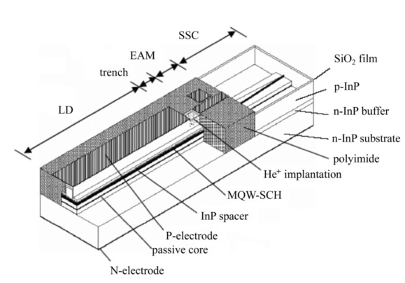
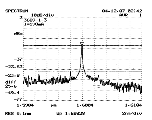
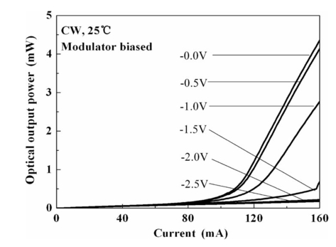
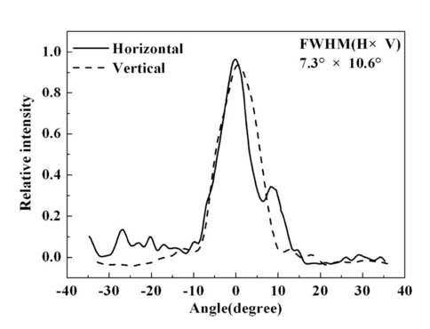
1.IntroductionMonolithic integration of a laser diode (LD) (or semiconductor optical amplifier) and an electroabsorption modulator (EAM) with a spot-size converter (SSC) output (LD-EAM-SSC) is very attractive for transmitter modules in optical fiber communication systems for its low-cost packaging due to its large spot size, which is well matched to that of a single-mode fiber (SMF). However, most of them have been based on buried structures1 or with butt-joint selective area growth,2 3 which involves complex growth steps, excessive processing steps, and strict process tolerance. In this letter, a 1.60-μm novel LD-EAM-SSC is demonstrated using a relatively simple fabrication approach in which selective area growth (SAG) and asymmetric twin waveguide (ATG) technologies were successively used. By contrast with butt-joint selective area growth, the SAG method is useful in fabricating several band edges across the wafer in a single epitaxial growth step, while the ATG approach allows a variety of photonic integrated circuits (PICs) with different layouts and components to be fabricated from the same wafer. All the integrated components are defined by postgrowth pattering, eliminating the need for epitaxial regrowth.4 In addition, ATG technology is robust, low-loss, compatible with existing epitaxial designs, and uses fabrication techniques that are common in InP laser manufacturing.5 As for our device, SAG technology was employed in the LD/EAM section to exactly control bandgap difference of the LD gain peak and exciton absorption edge while ATG technology was employed in the SSC sections to expand the mode spot size to match the core of a SMF. The active waveguide is laterally tapered and combined with an underling passive waveguide. Such a combination makes it easy to control the beam divergence at the output facet. For the device structure, in the LD/EAM section a double-ridge structure was employed to reduce the EAM capacitances and enable high-bit-rate operation. For the SSC sections, a buried ridge double-core structure (BRS) was incorporated. 2.Device Structure and FabricationThe schematic diagram of the device is shown in Fig. 1. The device consists of a 600-μm-long LD, a 50-μm-long etched electrical isolation, a 150-μm-long EAM, and a 300-μm-long dual-core SSC on the output end to improve the optical coupling efficiency. The device is fabricated using only a three-step low-pressure metal-organic vapor phase epitaxial (LP-MOVPE) process, the second of which is a SAG step. For the first epitaxial growth, InP buffer, 50-nm-thick n-type 1.15-μm bandgap InGaAsP quaternary (Q) lower waveguide and a 0.2-μm n-InP spacer layer are grown. Then, two SiO 2 pads are patterned on the spacer layer in the LD region. The multi-quantum well and separate confinement heterojunction (MQW-SCH) stack is then grown in the second epitaxial growth. The SAG process creates a bandgap difference between the modulator and the laser diode of 75 nm as measured with small-spot photoluminescence. After removing the SiO 2, the lateral taper is formed by selective etchant of MQW-SCH layers from the SSC regions. A thin P-InP cladding layer, 1.2Q etch stop layer, P-InP overcladding, and an InGaAs cap layer are then grown in the third epitaxial growth step. This is followed by conventional double-ridge waveguide processing of the LD/EAM sections. 3.Device PerformancesFigure 2 shows the laser typical optical spectra of the device at 198 mA and 25°C when the EAM biased voltage is 0 V. Quasi-single longitudinal mode was observed with a side mode suppression ratio (SMSR) of 25.6 dB, although no grating was fabricated in the LD region. The frequency response for the modulator was measured at −2 V of dc bias. The 3-dB bandwidth for the modulator is about 16 GHz. Figure 3 shows the L-I characteristics of the device when the modulator was biased. From these L-I characteristics, one can see that when the bias voltage on the modulator was varied from 0.0 to −2.0 V while the current injection on the laser was fixed at 160 mA, the on-off ratio was larger than 16.2:1. Figure 4 shows the far-field pattern observed from the SSC facet. The device emits in a single transverse mode, which indicated that there was no degradation of the single transverse mode characteristics with the introduction of the SSC. The divergence angles from SSC facet are as small as 7.3 deg (horizontal)×10.6 deg (vertical). In contrary, those from the rear facet of the LD are as large as 30.0 and 49 deg. The coupling loss and 1-dB align tolerance for the SSC facet are about 3.0 dB, ±3.1 μm (horizontal)×±2.65 μm (vertical), when the device was coupled to a cleaved SMF. However, at the same case, those from the rear facet of the LD are about 9 dB, ±2.0 μm (horizontal)×±1.7 μm (vertical). 4.ConclusionIn conclusion, a 1.60-μm laser diode and electroabsorption modulator monolithically integrated with a novel dual-core spot-size converter output for low-loss coupling to cleaved single-mode optical fiber is demonstrated. The devices emit in a single transverse and quasi-single longitudinal mode with SMSR of 25.6 dB. The dc extinction ratio of 16.2 dB is observed for the device with the modulator at −2 V of dc bias. The 3-dB modulation bandwidth of 16.0 GHz is also observed at the same case. The output beam divergence angles of the spot size were as small as 7.3 deg (horizontal)×10.6 deg (vertical), resulting in low-coupling losses with a cleaved optical fiber (3.0-dB loss). Simple fabrication procedure and excellent performance make the device suitable for mass production and a cost-effective active, or passive, mode-locked laser. AcknowledgmentThis project was supported by the National Natural Sciences Foundation of China under Grant No. 90101023 and the Special for Major State Basic Research Project of China under Grant No. 20000683-1. REFERENCES
U. Koren
,
B. I. Miller
,
M. G. Young
et al.;,
“Polarization insensitive semiconductor optical amplifier with integrated electroabsorption modulators,”
Electron. Lett. , 32
(2), 111
–112
(1996). Google Scholar
M. Beck
,
O. Abdallah
, and
W. L. Charles
,
“40-Gb/s tandem electroabsorption modulator,”
IEEE Photonics Technol. Lett. , 14
(1), 27
–29
(2002). Google Scholar
K. Asaka
,
Y. Suzaki
, and
Y. Kawaguchi
,
“Lossless electroabsorption modulator monolithically integrated with a semiconductor optical amplifier and a passive waveguide,”
IEEE Photonics Technol. Lett. , 15
(5), 679
–681
(2003). Google Scholar
J. E. Johnson
,
L. J. P. Ketelsen
, and
J. A. Grenko
,
“Monolithically integrated semiconductor optical amplifier and electroabsorption modulator with dual-waveguide spot-size converter input,”
IEEE J. Sel. Top. Quantum Electron. , 6
(1), 19
–25
(2000). Google Scholar
|