|
|
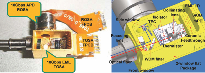
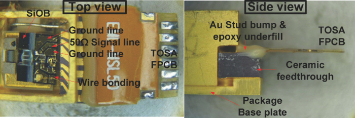
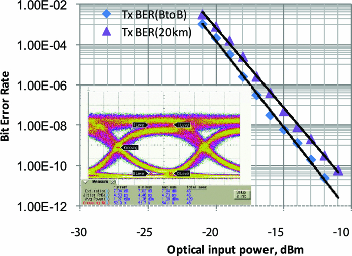
1.IntroductionHigh bandwidth services have strongly driven fiber-to-the-home networks to adopt a 10-Gbps passive optical network (PON) system as their access network. In these networks, a bidirectional communication system has typically been introduced for PON systems in order to reduce the network construction and maintenance costs. In a previous study, 10-Gbps bidirectional optical subassembly (BOSA) techniques for optical network units were constructed by combining a TO-can-packaged transmitter optical subassembly (TOSA) and receiver optical subassembly (ROSA) to a metal housing via a laser welding technique.1 In general, the metal housing containing a lens, filter, and fiber is firmly mounted on a transceiver package and supports the BOSA structure, which is widely used to take an uncooled laser, such as a distributed feedback laser in a TOSA. However, we need to consider the laser cooling issue of an electroabsorptive modulated laser (EML) BOSA for 10-Gbps optical line terminal (OLT) applications. An EML typically needs a thermoelectric cooler (TEC) to stabilize the wavelength and optical output power. Thus, dissipation of the TEC joule heat is the most important consideration in designing an EML BOSA structure. To efficiently dissipate the TEC joule heat, the base plate of the EML BOSA package is generally fabricated using copper tungsten (CuW), and should be tightly mounted on a transceiver package. Thus, most components not contained in the EML TOSA package such as metal housings, filters, and lenses are jointed at the window of the EML TOSA package using a laser welding technique. As such, in terms of mechanical reliability, the weight on the welding joint should be minimized in order to reduce mechanical stress incurred by external mechanical shock and vibration. Based on the above points, an EML BOSA structure that considers TEC heat dissipation and mechanical reliability should be developed. In this letter, we introduce an EML BOSA based on a novel two-window flat package that reduces stress on welded joints and enhances TEC joule heat dissipation by simplifying the BOSA structure. 2.Structure and Fabrication of 10-Gbps EML BOSAFigure 1 shows the fully assembled 10-Gbps EML BOSA. Components such as the EML chip, TEC, thermistor, isolator, and filter are integrated inside the two-window flat package, thereby simplifying the EML BOSA structure; the manufacturing cost is reduced by removing the need for separate TOSA and ROSA metal housings. The length, height, and width of the two-window flat packages are 11, 5.8, and 5.8 mm, respectively, which are compatible with a standard microdevice (XMD) mini flat package. The optical output signal, emitted by an EML chip having a 1577 nm wavelength, passes through a 45° wavelength division multiplexing (WDM) filter, and is coupled to a fiber at the front window of the two-window flat package. The optical input signal, having 1270 nm wavelength, enters the package through the front window, is reflected by the 45° WDM filter, and changes direction to become perpendicular to the input beam path. The optical input signal then passes through the side window of the two-window flat package, and couples to an avalanche photodiode (APD) chip in the ROSA. Here, a silicon optical bench (SiOB) is fabricated on high resistivity silicon. The SiOB is a cost-effective technology for mass production, and has recently become widely used as an optical component platform.2 On the SiOB platform, a V-groove for lens assembly is fabricated via a 410-μm depth wet-etching process; the patterns are then fabricated using a thin-film metallization process. The EML chip, monitoring photodiode, and thermistor are flip-chip bonded on the SiOB platform with AuSn solder at 280°C. On the V-groove, a 1-mm diameter collimating microaspheric lens is integrated with flip-chip bonding using a low outgassing epoxy resin. Note that the placement accuracy of the lens should be smaller than ±2 μm to ensure a collimated beam size of ∼550 μm; based on this design, we achieved an optical coupling efficiency of around 60% by placing the microaspheric lens at a distance of 160 μm to the emitting side of the EML in order to reduce spherical aberrations. The TEC is bonded on the CuW base plate of a two-window mini flat package using low-melting-temperature indium solder, which is also used to bond the previously assembled SiOB substrate onto the TEC. A single-stage optical isolator—very sensitive to temperature change—is bonded onto the TEC using silver epoxy and a thin-film WDM filter is placed in front of the optical isolator to split the optical input and output signals depending on the wavelength. Figure 2 presents the signal transmission and electric power supply line connected from the SiOB substrate to the external flexible printed circuit board (FPCB). The signal line connecting the electroabsorptive modulation part of the EML chip is fabricated with thin-film Ni-Cr to have a 50 Ω matching resistance. A ceramic feed-through of the package is fabricated using a high temperature co-fired ceramic (HTCC). A gold (Au) stud bump is fabricated on the ceramic feed-through using a commercial wire bonder. Then, the FPCB is flip-chip bonded on the Au stud bump, and fixed using an underfill epoxy resin. As a result, a high-speed electrical signal can be transmitted from the FPCB to the SiOB platform via the ceramic feed-through with no bending or sharp turns, such that the signal transmission loss is minimized. The APD ROSA comprised of an APD chip and transimpedance amplifier is packaged in a commercial TO-46 package. The FPCB is connected to the co-axial lead pin of the TO-46 package. To minimize optical crosstalk, a blocking filter with a 40 dB optical isolation was installed at the window of the APD ROSA. The subassembled EML TOSA is aligned with a fiber by detecting the optical output power, and fixed using laser welding. Then, the APD ROSA is placed at the side window of the EML TOSA package, and aligned to the position at which the maximum APD photocurrent is detected for the optical input power. 3.Experimental ResultsThe optical output power of the EML TOSA was over 8 dBm, and the side-mode suppression ratio was over 35 dB at a 25°C ambient temperature and 50 mA input bias current. The –3 dB modulation bandwidth of the EML TOSA was over 9 GHz, and the signal return loss was less than –10 dB at 9 GHz. Figure 3 shows the bit error rate (BER) test results for 10-Gbps transmission; both the rise and fall times were less than 60 ps, the extinction ratio was over 7 dB, and the dispersion penalty at 20 km transmission was less than 1.5 dB. Figure 4 shows the BER test results of the APD ROSA, in which the sensitivities were less than –21.5 dBm at a BER of 10−12, and –27 dBm at a BER of 10−3 without forward error correction (FEC), for a 10-Gbps optical input signal. In this experiment, the APD ROSA responsivity was less than 0.5 A/W. To test the signal crosstalk, the sensitivities were measured for the on/off states of the EML TOSA power. Compared to the sensitivity measured under the “off” state, the sensitivity for the “on” state incurred a 1.2 dB crosstalk penalty. Changes of the EML TOSA power and APD ROSA responsivity were less than 0.5 dB measured before and after a mechanical shock test under conditions of 500 G peak acceleration and 1 ms pulse duration, which satisfied a mechanical reliability criterion of Telcordia GR-468-CORE. The EML BOSA was operated at a temperature range of 0°C to 75°C using a thermal chamber to evaluate a cooling performance of the TEC. The EML chip temperature was successfully controlled at 45°C with an EML input bias current of 100 mA, and the maximum power consumption was lower than 0.45 W at an operating temperature of 75°C. 4.ConclusionsA 10-Gbps EML BOSA comprised of an EML TOSA and APD ROSA for a 10-Gbps PON OLT system was successfully fabricated and demonstrated by introducing a novel XMD compatible two-window flat package in an attempt to enhance the mechanical reliability and cooling performance. Based on this design, the optical output power was over 8 dBm with a 50 mA input bias current at 25°C operating temperature due to a high coupling efficiency of over 60%. The extinction ratio was over 7 dB, and the dispersion penalty was less than 1.5 dB at 20 km transmission. The APD ROSA sensitivity was –21.5 dBm at a BER of 10−12 and –27 dBm at a BER of 10−3 without FEC, and the sensitivity penalty due to the signal crosstalk was less than 1.2 dB. In addition, the EML BOSA passed a shock test under conditions of 500 G peak acceleration and 1 ms pulse duration, and the TEC consumed a power of less than 0.45 W to control the EML chip temperature at 45°C for a temperature range from 0°C to 75°C. ReferencesT.-T. Shih, M.-C. Lin, P.-H. Tseng, C.-Y. Li, T.-Y. Hung, Y.-J. Chiu, and W.-H. Cheng,
“High-performance and low-cost 10-Gb/s bidirectional optical subassembly modules,”
J. Lightwave Technol., 11
(25), 3488
–3494
(2007). https://doi.org/10.1109/JLT.2007.907786 Google Scholar
J. J. Lee, K.-S. Lim, S. Lee, and H. S. Kang,
“Compact bidirectional optical subassembly vertically stacked with 1.25-Gbps transmitter and 10-Gbps receiver for passive optical networks,”
Opt. Eng., 49
(11), 110501
(2010). https://doi.org/10.1117/1.3506718 Google Scholar
|