|
|
|
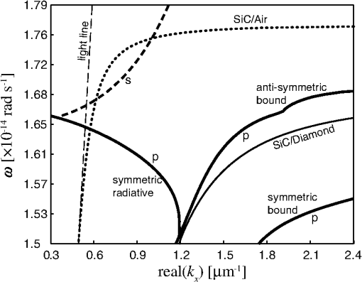
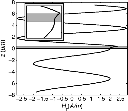
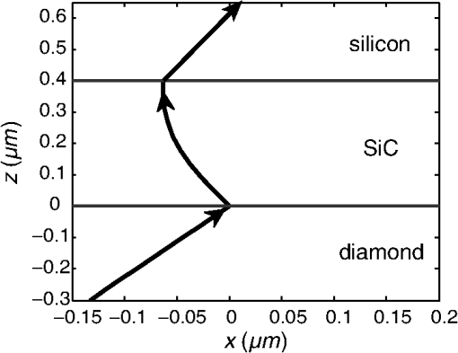
Currently, there is great interest in materials that refract light negatively. Negative refraction can be characterized by a light beam whose wavefront is refracted normally (in a positive direction), while its energy flux is refracted negatively. Materials that negatively refract light can enable applications such as near-field superlensing and optical cloaking.1 Approaches to developing negative refraction materials include the design of photonic crystals with geometries that result in desired dispersion properties. The photonic crystal approach has produced some notable successes in the development of microwave to infrared negative refraction materials.2,3 Another approach is to exploit material resonance modes to achieve negative refraction.4,5 Recent examples include the use of infrared plasma resonance in free-carrier doped InGaAs films to suport negative refraction.6 Magnetic resonance, in gold, has also been applied to the development of mid-IR negative refraction materials.7 In this letter, we propose that coupled photon-phonon resonance modes, called radiative surface phonon polaritons (RSPhP), can be exploited in the development of mid-IR negative refraction materials. To demonstrate this idea, we present theoretical results for a prototype structure consisting of a thin silicon carbide (SiC) film, bounded by very thick layers of silicon (Si) and diamond (Di). Approaches to achieving mid-IR negative refraction materials are necessary for the development of next-generation thermal management devices such as thermal rectifiers and specialized thermal emitters.8,9 Physically, surface phonon polaritons are atomic lattice-waves coupled to transverse magnetic (-polarized) electromagnetic fields that may be supported at the interface between a polar material bounded by a dielectric. For example, surface phonon polaritons can be excited at the interface between air (dielectric constant, ) and a semi-infinite layer of SiC [a polar material with a frequency varying dielectric function ]. The SiC/Air system is illustrated in Fig. 1(a), and the well-known dispersion relation for surface phonon polariton modes at an interface formed between a semi-infinite polar material and a dielectric is given by the expression where the dependency on frequency is made explicit and where is the speed of light. The surface phonon polariton dispersion relation for the SiC/Air case is plotted as the dotted line in Fig. 2. The vertical axis of Fig. 2 is the frequency at which the surface mode exists and the horizontal axis is (the real part of) , which is the wavevector for the surface polariton that is propagating parallel to the SiC interface. The “light line” is the dashed diagonal line through the plot and gives the dispersion relation for light propagation in free space, or . The upper and lower limits of the frequency axis, in Fig. 2, approximately correspond to the spectral locations of the SiC transverse optical frequency and its longitudinal optical frequency , which gives the SiC/Air polariton dispersion cutoff. Between these frequency limits, the dielectric function of SiC is less than zero, i.e. , and a negative dielectric indicates that the material may support electromagnetic resonance modes. More specifically, the SiC dielectric function can be described by the Lorentz model where , , , and the damping constant is given as . In this letter, the loss term is included in all calculations.Fig. 1(a) Schematic of semi-infinite SiC/Air system. (b) Schematic of Si/SiC/Di structure studied in this work, where is the SiC thickness, and is the angle of the incident light.  Fig. 2Frequency versus the real part of . Thin Dashed Line: Free space light line. Dotted Line: SPhP dispersion relation for semi-infinite SiC bounded by air [Fig. 1(a)]. Solid Thick Lines: SPhP dispersion relation for -polarized light in multilayer structure shown in Fig. 1(b). Thick Dashed Line: Dispersion relation for -polarized light in the multilayer structure. Thin Solid Line: Dispersion relation for semi-infinite SiC bounded by diamond.  The wavevector representing the component of light propagating perpendicular to ’th interface is defined by . Therefore, surface modes with cannot couple to propagating light, since would be purely imaginary. Figure 2 shows that the surface phonon polariton mode for the SiC/Air structure is to the right of the light line and, thus, is too large for a beam of incident light to interact with the surface phonon polariton. So, while it is possible for semi-infinite SiC to support mid-IR surface phonon polaritons, these modes are forbidden from direct coupling to propagating light. However, the situation completely changes for the case of a thin, 400 nm layer of SiC, sandwiched between semi-infinite thick layers of Si and diamond, as shown in Fig. 1(b). These materials were chosen because they are transparent in the infrared region and have high refractive indexes with and . The dispersion relation, for surface phonon polaritons in the Si/SiC/Di structure, is determined by numerically finding values of that result in zeros for the denominator of the three-layer, -polarized, reflectance equation,10 where , and the subscripts refer to the layers and 2, where diamond is layer 0, SiC is layer 1, and Si is layer 3. The numerically determined surface phonon polariton dispersion relation for the Si/SiC/Di structure is given by the solid thick lines of Fig. 2, and shows three branches. Two branches are completely to the right of the light line and represent modes unaccessible by propagating light. As shown in the figure, the two modes are the antisymmetric and symmetric modes which are well-known to represent the surface polaritons at each interface the thin film.10 The plot also shows the dispersion relation for semi-infinite SiC bounded by diamond. While the horizontal axis range is limited in Fig. 2 for brevity, previous theoretical results suggest that for very large , degeneracy is lifted and the symmetric and anti-symmetric modes become equivalent to the semi-infinite SiC/Diamond case. The SPhP modes are known to only exist for the -polarized case. For comparison, we also plot the dispersion relation for the -polarized case in Fig. 2 to show that the effects discussed in this letter only occur for -polarized light.The third branch of the Si/SiC/Di dispersion relation extends to the left of the light line, crossing it at approximately , or 11.4 μm. Since this mode crosses the light line and is, thus, accessible by propagating light with a wavelength of about 11.4 μm, we refer to it as a radiative surface phonon polariton (RSPhP). As will be shown below, calculation of the magnetic field shows that the mode is symmetric since the transverse component of the electric field () is not zero inside the film [c.f. Fig. 3 and Eq. (4)]. Symmetric (and anti-symmetric) radiative surface polaritons have been predicted, before, for the case of multilayer structures. However, our calculations show that the radiative branch of the dispersion relation presented here has a negative slope. Since the group velocity is given by , the negative slope implies a negative group velocity. Also, since the group velocity characterizes the direction of energy flow, which in this case is roughly opposite of the wave propagation direction (), negative refraction may be possible with the structure shown in Fig. 1(a). To validate that the radiative mode is a physical solution, we calculated the imaginary part of for the RSPhP mode as positive. Thus, the surface mode decays as it propagates along the film, radiating light into the silicon along the way. Fig. 3Magnetic field distribution in three layer structure at 11.4 μm. Inset: Details of magnetic field inside SiC layer.  In the remainder of this letter, we will use theoretical evidence to support the idea that incident light coupling to radiative surface phonon polariton modes can be accomplished in the Si/SiC/Di structure. We also use theoretical results to show that negative refraction is occurring in the SiC layer of the Si/SiC/Di structure. We can characterize this light coupling by examining the magnetic field in the Si/SiC/Di structure. Referring to the system shown in Fig. 1(b), we start by describing the magnetic field in each layer as The boundary conditions require that the magnetic fields and their derivatives be continuous at each interface, e.g., , and at . By manipulating Eqs. (4) through (6) and applying the attendant boundary conditions, we find The magnetic field is plotted for the case of 11.4 μm light in Fig. 3, where the gray region represents the SiC layer.Figure 3 shows the infrared light propagating through the diamond layer as an oscillating field below the gray region. The gray region is the SiC layer. Figure 3 also shows the field exponentially decaying within the SiC layer, which is characteristic of a surface phonon polariton mode. The inset of Fig. 3 shows the details of the exponential decay in the SiC layer. Finally, another oscillating field is shown in the region above the SiC region, which demonstrates that the RSPhP mode is leaking into the silicon layer. Furthermore, the results show that the RSPhP mode is not self-sustaining, but depends on infrared light incident from the diamond side.11 We now, theoretically, show that the 11.4 μm light energy flux is negatively refracted in the Si/SiC/Di structure. The Poynting vector describes the light energy flux as and thus the direction of the energy flux in the material is given by where the magnetic fields are given by Eqs. (4) through (6), and Maxwell’s equations give the associated electric fields as which when used with Eq. (9) for each layer, we obtain The energy flux directions for -polarized 11.4 μm light in Si/SiC/Di is plotted in Fig. 4.Figure 4 shows that the energy flux has a positive incidence angle at the SiC/Di interface which we calculate from Eq. (11) to be . The energy flux then, dramatically, changes its angular direction in the SiC such that it is negatively refracted as it propagates from the diamond to the Si/SiC interface. The flux angle in the SiC layer, , is calculated using Eq. (12). The real part of varys from to , and is plotted in Fig. 4. The curvature of the energy flux in the SiC layer is consistent with Fermat’s principle, since there is significant variation in refractive index from the diamond to Si layers. The energy flux emerges from the SiC/Si interface again with a positive angle calculated, with Eq. (13), to be . In conclusion, this letter, theoretically, predicts that a submicron thin film of SiC, bounded by silicon and diamond, may be used as a negative refraction material. The key mechanism is the radiative surface phonon polariton mode coupled to incident light at the SiC interfaces. AcknowledgmentsThis work was supported by AFRL through a subcontract with Universal Technology Corporation, subcontract No. 11-S567-0015-02-C6. ReferencesS. KawataY. InouyeP. Verma,
“Plasmonics for near-field nano-imaging and superlensing,”
Nat. Photonics, 3
(7), 388
–394
(2009). http://dx.doi.org/10.1038/nphoton.2009.111 1749-4885 Google Scholar
A. Berrieret al.,
“Negative refraction at infrared wavelengths in a two-dimensional photonic crystal,”
Phys. Rev. Lett., 93
(7), 73902
(2004). http://dx.doi.org/10.1103/PhysRevLett.93.073902 PRLTAO 0031-9007 Google Scholar
E. Schonbrunet al.,
“Wave front evolution of negatively refracted waves in a photonic crystal,”
Appl. Phys. Lett., 90
(4), 041113
(2007). http://dx.doi.org/10.1063/1.2435344 APPLAB 0003-6951 Google Scholar
J. Yaoet al.,
“Optical negative refraction in bulk metamaterials of nanowires,”
Science, 321
(5891), 930
–930
(2008). http://dx.doi.org/10.1126/science.1157566 SCIEAS 0036-8075 Google Scholar
V. Shalaev,
“Optical negative-index metamaterials,”
Nat. photonics, 1
(1), 41
–48
(2007). http://dx.doi.org/10.1038/nphoton.2006.49 1749-4885 Google Scholar
A. Hoffmanet al.,
“Negative refraction in semiconductor metamaterials,”
Nat. Mater., 6
(12), 946
–950
(2007). http://dx.doi.org/10.1038/nmat2033 NMAACR 1476-1122 Google Scholar
J. Bossardet al.,
“Synthesizing low loss negative index metamaterial stacks for the mid-infrared using genetic algorithms,”
Opt. Express, 17
(17), 14771
–14779
(2009). http://dx.doi.org/10.1364/OE.17.014771 OPEXFF 1094-4087 Google Scholar
S. BasuM. Francoeur,
“Near-field radiative transfer based thermal rectification using doped silicon,”
Appl. Phys. Lett., 98
(11), 113106
(2011). http://dx.doi.org/10.1063/1.3567026 APPLAB 0003-6951 Google Scholar
C. FuZ. Zhang,
“Further investigation of coherent thermal emission from single negative materials,”
Nanoscale Microsc. Thermophys. Eng., 12
(1), 83
–97
(2008). http://dx.doi.org/10.1080/15567260701866744 NMTECW 1556-7265 Google Scholar
H. Raether, Surface Plasmons on Smooth and Rough Surfaces and on Gratings, Springer, Berlin
(1988). Google Scholar
J. BurkeG. StegemanT. Tamir,
“Surface-polariton-like waves guided by thin, lossy metal films,”
Phys. Rev. B, 33
(8), 5186
(1986). http://dx.doi.org/10.1103/PhysRevB.33.5186 PRBMDO 0163-1829 Google Scholar
|


