|
|
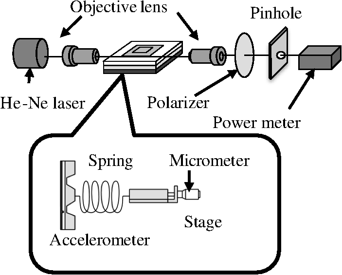
1.IntroductionSilicon-based guided-wave optical sensors with micromechanical structures, such as diaphragm and cantilever, have continued to attract attention due to the remarkable development of MEMS and MOEMS technologies, and have been actively proposed and demonstrated since the late 1980s.1–6 Our group also has been developing silicon-based guided-wave optical pressure sensors,7,8 microphones, accelerometers,9 and flow sensors with diaphragms. These sensors have two unique features: guided-wave optical sensing and the use of micromechanical structures. The guided-wave optical sensing provides several advantages, such as immunity to electromagnetic interference and the impossibility of electrical leak. Thus, the sensors can be utilized even in harsh environments, such as industrial plants and power plants, without any special protection against electromagnetic interference or electrical leak. Incidentally, silicon has excellent micromechanical properties, and various micromechanical structures are available on silicon substrates.10 Excellent features of micromechanical structures, such as being lightweight and adaptable to miniaturization, can be added to sensing devices, thus expanding the application of guided-wave optical sensors to mechanical sensing, such as pressure, fluid flow, and acceleration sensing. In industrial plants and power plants, accelerometers can be significant in the detection of abnormal vibration due to malfunction and in the monitoring of machine operations. Our group has proposed a silicon-based guided-wave optical accelerometer, which consists of a micromachined diaphragm with a proof mass and a single-mode waveguide on the diaphragm. For accelerometers, sensitivity, frequency response, and resonance frequency are very significant as sensor specifications. Sensitivity and resonance frequency are strongly suggested to be related to waveguide location, diaphragm size, mass weight, etc. These relationships should be determined theoretically and experimentally in order to establish a design guideline. In this study, sensitivity dependences on waveguide position and diaphragm thickness were examined experimentally. The experimental results suggest that sensitivity is highest at the diaphragm edge and is inversely proportional to the square of diaphragm thickness. The findings of this study are quite reasonable according to our knowledge of a guided-wave optical pressure sensor with a diaphragm.8,11,12 2.Principles of Sensor OperationFigure 1 shows a silicon-based guided-wave optical accelerometer, consisting of a diaphragm with a proof mass and a straight single-mode waveguide on the diaphragm. An intermodal interferometer using a straight waveguide was used in this study since formation of a number of waveguides on the diaphragm was required to investigate sensitivity dependence on waveguide position. This interferometer, however, would be better if replaced with a Mach-Zehnder interferometer, a Michelson interferometer, or a ring resonator in practical use. Fig. 1(a) Schematic drawing of a silicon-based guided-wave optical accelerometer between a pair of crossed polarizers, and (b) its cross-section view. 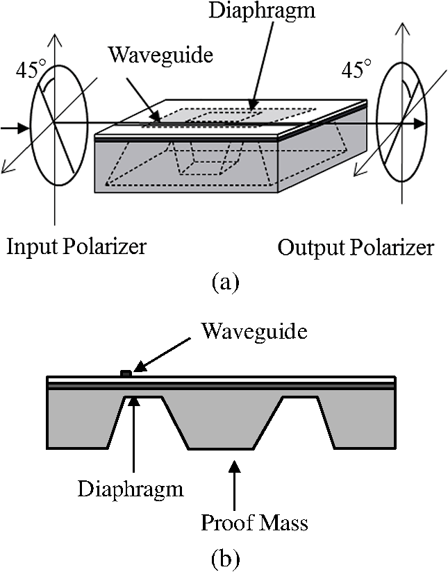 When acceleration is applied to the sensor, the diaphragm is distorted by inertial force. The distortion causes strain, which induces a change in the refractive index of waveguide by the elasto-optic effect. The index change produces phase retardation in the lightwave, which propagates in the waveguide on the diaphragm. Since the phase retardation is dependent on the guided modes, the phase difference between the fundamental transverse magnetic (TM)-like and transverse electric (TE)-like modes is also a function of the applied acceleration. To detect the phase difference, the sensor is placed in a pair of crossed polarizers as shown in Fig. 1(a). The input polarizer is oriented at 45 deg with respect to the sensor surface. The light beam from the input polarizer is coupled to the fundamental TM-like and TE-like modes at equal intensities. At the end of the waveguide, the lightwave has linear, elliptic, or circular polarization, corresponding to the induced phase difference between the two guided modes. The crossed output polarizer converts the polarization-modulated light into intensity-modulated light. The intensity of the beam passing through the output polarizer sinusoidally changes in response to inertial force, corresponding to the magnitude of acceleration. Therefore, the acceleration exerted to the sensor can be determined from the output intensity. 3.Sensitivity Dependence on Waveguide Position3.1.Fabrication and Experimental SetupFigure 2 shows a fabricated optical accelerometer with actual dimensions. In order to investigate sensitivity dependence on waveguide position, 17 straight ridge-type polystyrene waveguides spaced 0.25 mm apart were formed on both sides of a diaphragm. Figure 2(d) indicates a cross-sectional view of the waveguide. Width of the waveguide was 7.0 μm, and thickness of the polystyrene guided layer at the waveguide was 1.1 μm, thicker by 0.1 μm than the surroundings. Thickness of the buffer layer was determined to be 1.0 μm in order to sufficiently reduce the radiation loss of the guided waves into the silicon with high refractive index. On the top surface, the area of the diaphragm and proof mass were and , respectively. Also, the thicknesses of the diaphragm and proof mass were 50 and 300 μm, respectively. The overall dimensions of the sensor were 20 mm long, 20 mm wide and 300 μm thick. Fig. 2(a) Cross-sectional view and (b) bottom view of a fabricated guided-wave optical accelerometer and (c) cross-section of a ridge-type polystyrene waveguide. 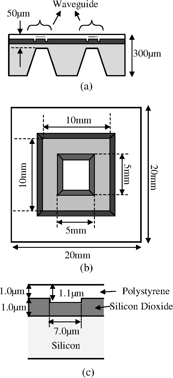 In fabrication, a silicon substrate was first thermally wet-oxidized at 1100°C to form a silicon dioxide layer. The silicon dioxide layer of the bottom surface was selectively removed by an etchant of buffered HF acid, using a patterned photoresist as an etching mask. During etching, the silicon dioxide of the top surface was protected by a thick layer of electron wax. Then, the exposed silicon was anisotropically etched in aqueous KOH solution at 50°C to form the diaphragm. Diaphragm thickness was controlled by etching time. After diaphragm formation, the silicon dioxide layer 1.0 μm thick was regrown by thermal oxidation to serve as a buffer layer. Shallow 7.0 μm-wide and 0.1 mm-deep grooves were engraved on the silicon dioxide layer, parallel to the diaphragm edge, using buffered HF acid. The polystyrene layer was spin-coated as the guided layer, and its thickness at the grooves was 1.1 μm. Figure 3 shows the experimental setup to measure output power as a function of applied force, as simulated inertial force due to acceleration. A linearly polarized He-Ne laser at 633 nm in wavelength was used as the light source. The polarization of the laser beam was set at 45 deg to the sensor surface, so that the input polarizer was not utilized during measurement. A pinhole was placed in front of a photodetector to block stray light. In this study, rather than inertial force by acceleration, static force directly applied on the proof mass by a spring connected to a micrometer was used since valuable data to consider sensitivity dependences can be sufficiently obtain even from static response. 3.2.Experimental ResultsIn order to examine sensitivity dependence versus waveguide position, sensitivity was measured for each waveguide formed on the diaphragm. Here, phase sensitivity is used as sensor sensitivity, which is defined as the induced phase difference between the two modes per unit force or unit gravity. Phase sensitivity can be evaluated from a half period of the output power as a function of the applied force, since a half period corresponds to a phase difference of rad. Figure 4 shows examples of normalized output power versus the applied force. Figure 4(a) and 4(b) is for waveguide positions nearest the edges of the diaphragm and proof mass, respectively. Dots represent measured values, and the sinusoidal curves indicate the computer projection of the experimental data. The measured output power sinusoidally changes in response to the applied force. A half period of the output power is called the half-wave force and corresponds to the dynamic range. The half-wave force is equivalent to the phase difference of rad. From Fig. 4(a) and 4(b), the half-wave forces were evaluated to be 7.1 and 16 mN, and the phase sensitivities in radian per milli-Newton were calculated 0.44 and from the measured half-wave force, respectively. Moreover, phase sensitivity in milli-radian per gravity is estimated to be 76 and when the mass of the proof mass is 17.5 mg (). Incidentally, the extinction ratios were quite low mainly due to undesired stray light passing through the pinhole. A low extinction ratio does not affect sensitivity dependence, but it should be improved for practical use. Fig. 4Phase sensitivity as a function of applied force for the waveguides (a) nearest the diaphragm edge and (b) nearest the edge of the proof mass. 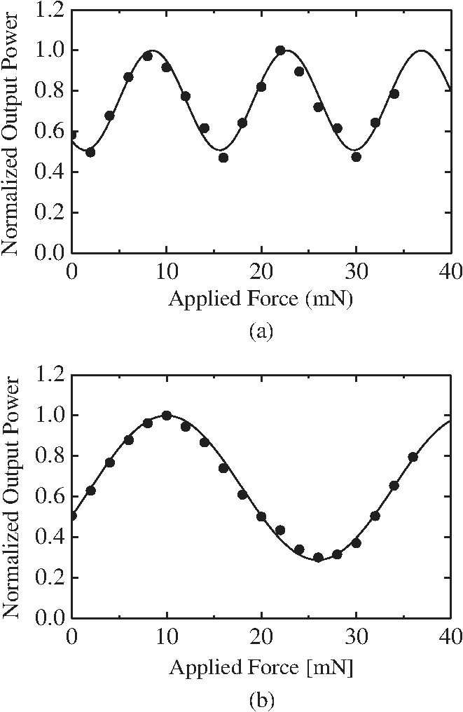 Figure 5 shows the evaluated phase sensitivity versus waveguide position. In the graph, positions of and correspond to the diaphragm edges and the edges of the proof mass, respectively. From the figure, phase sensitivity is highest when the waveguide is placed along the diaphragm edge. Moreover, sensitivity is relatively high for the waveguide along the edge of proof mass and is very low between the edges of the diaphragm and the proof mass. Therefore, to maximize sensitivity, the diaphragm edge is the best waveguide position. Fig. 5Phase sensitivity as a function of waveguide position for an accelerometer with a 10 mm-square, 50 μm-thick diaphragm and a 5 mm-square, 300 μm-thick proof mass. 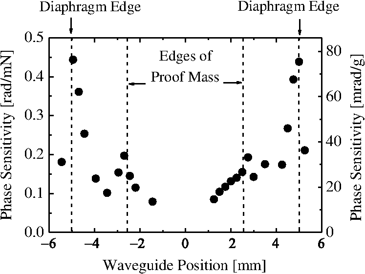 This sensitivity dependence is quite similar to the results of some guided-wave optical pressure sensors with a diaphragm5,11 if the edge of proof mass is set relative to the center of diaphragm of the pressure sensor. However, the sign of the sensitivity cannot be distinguished simply from the experimental data. According to the theoretical analysis of the pressure sensor, the sign of the sensitivity at the diaphragm edge must be opposite to that at the center of diaphragm.11 When inertial force is exerted to the accelerometer, if deflection around the diaphragm edge is convex, then deflection around the edge of the proof mass is concave, and vice versa. So, the sign of the sensitivity at the diaphragm edge would be opposite to that at the edge of the proof mass although the sensitivities at the edges of diaphragm and proof mass are both high with the same sign in Fig. 5. Hence, it may be possible to improve sensitivity by a push-pull configuration, which can be realized by a Mach-Zehnder interferometer, with paths along the edges of diaphragm and proof mass. 4.Sensitivity Dependence on Diaphragm Thickness4.1.FabricationFigure 6 shows fabricated optical accelerometers with actual dimensions. In order to examine sensitivity dependence on diaphragm thickness, two accelerometers for each diaphragm thickness of 50, 60, 70, 80, and 90 μm were fabricated. Thirty-five straight waveguides spaced 0.1 mm apart were formed on both sides of a diaphragm to confirm the sensitivity nearest the diaphragm edge. Although waveguide structure does not affect sensitivity dependences, strip-loaded-type BK7 waveguides were used in this experiment. Figure 6(d) shows a cross-sectional view of the waveguide. Thickness of the BK7 guided layer was 1.2 μm. Thickness and width of the loaded strip were 0.4 and 8.0 μm, so that the waveguide width was 8.0 μm. Thickness of the buffer layer was determined to be 1.4 μm in order to sufficiently reduce the radiation loss of the guided modes into the high-index silicon. On the top surface, the area of the diaphragm and 300 μm-thick proof mass were and , respectively. The overall dimensions of the sensor were 20 mm long, 20 mm wide, and 300 μm thick. Fig. 6(a) Cross-sectional view and (b) bottom view of fabricated guided-wave optical accelerometers and (c) cross-section of a strip-loaded-type BK7 waveguide. 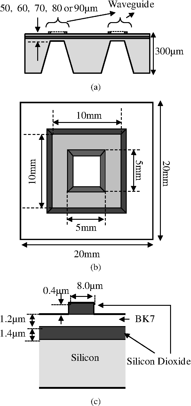 In fabrication, a diaphragm was first formed on a silicon substrate as described in Sec. 3.1. After diaphragm formation, the silicon dioxide was removed from the substrate in order to form strip-loaded-type waveguides on the diaphragm, following redeposition of a 1.4 μm-thick silicon dioxide film by sputtering as a buffer layer. Then, a 1.2 μm-thick BK7 glass film was deposited as the guided layer by sputtering. Moreover, 8 μm-wide and 0.4 μm-thick silicon dioxide strips were formed on the guided layer parallel to the diaphragm edge by sputtering and lift-off method. Experimental setup and measurement were same as described in Sec. 3.1. 4.2.Experimental ResultsFigure 7 shows normalized output power for the waveguide location nearest the diaphragm edge as a function of the applied force for fabricated accelerometers of diaphragm thicknesses, 50, 70, and 90 μm. In the figures, dots represent measured values, and sinusoidal curves indicate the computer projection of the experimental data. From Fig. 7(a)–7(c), the half-wave forces are evaluated to be 5.8, 11, and 18 mN, corresponding to phase sensitivities in radian per milli-Newton of 0.54, 0.28, and , respectively. Moreover, phase sensitivity in milli-radian per gravity is estimated to be 93, 49, and when the mass of the proof mass is 17.5 mg. Figure 8 shows phase sensitivity versus diaphragm thickness. Dots represent the evaluated phase sensitivities, and the line indicates the regression line for the experimental data. The slope of the regression line is in a log-log graph. Therefore, the phase sensitivity is experimentally determined to be inversely proportional to the square of the diaphragm thickness. Sensitivity can be adjusted in the 10’s mrad/g range for accelerometers with a diaphragm and a proof mass by designing the diaphragm thickness although the frequency range also varies. When detailed sensitivity dependences on dimensions of diaphragm and proof mass are determined theoretically and experimentally in the on-going study, they are expected to expand the designable sensitivity range. Fig. 7Normalized output powers versus applied force for (a) 50 μm-, (b) 70 μm- and (c) 90 μm-thick diaphragms. 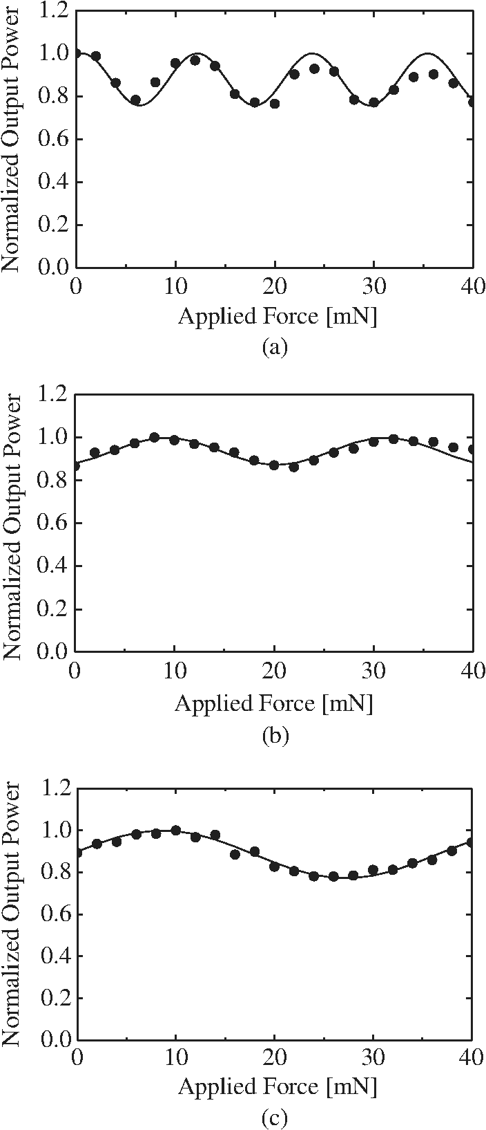 Fig. 8Evaluated phase sensitivity as a function of diaphragm thickness for accelerometers with a 10 mm-square, 50 μm-thick diaphragm and a 5 mm-square, 300 μm-thick proof mass. 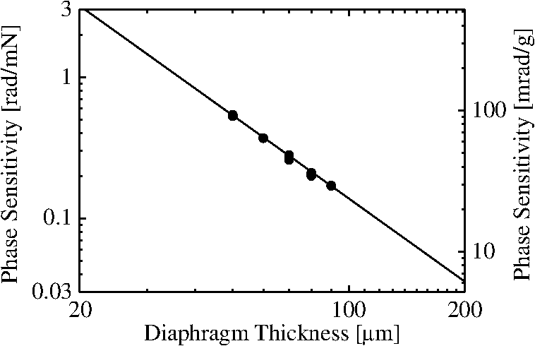 Incidentally, flexural rigidity of the diaphragm is defined as , where , , and denote the modulus of elasticity, Poisson’s ratio, and diaphragm thickness, respectively.13 Hence, flexibility of the diaphragm is inversely proportional to the cube of the diaphragm thickness. In addition, strain at the diaphragm surface, where a waveguide is formed, is known to be proportional to the diaphragm thickness, while the curvature of the diaphragm is kept constant. From both effects, sensitivity is expected to be inversely proportional to the square of the diaphragm thickness. Such sensitivity dependence has been identified in previous theoretical and experimental studies of the pressure sensor.8,12 The results shown in this section agree well with the findings of the pressure sensor8,12 and are quite reasonable, although the accelerometer has a thick proof mass. 5.ConclusionsSensitivity dependences on waveguide position and diaphragm thickness were experimentally examined for a silicon-based guided-wave optical accelerometer. Regarding sensitivity dependence on waveguide position, the highest phase sensitivity was obtained for the waveguide located at the diaphragm edge. It is found that to maximize sensitivity, the diaphragm edge is the best waveguide position. Regarding sensitivity dependence on the diaphragm thickness, phase sensitivity was found to be inversely proportional to the square of diaphragm thickness. For accelerometers with a diaphragm and a proof mass, the phase sensitivities in the range could be realized by changing diaphragm thickness of 10’s μm, for example, when diaphragm thickness is 50 μm. These findings regarding sensitivity dependences are quite reasonable according to our knowledge of guided-wave optical pressure sensors and provide very valuable information in the designing of accelerometers, although theoretical considerations are necessary to identify sensitivity dependences. AcknowledgmentsThis work is, in part, supported by a Grant-in-Aid for Scientific Research (No. 22560322) from the Japan Society for the Promotion of Science. ReferencesM. OhkawaM. IzutsuT. Sueta,
“Integrated optic pressure sensor on silicon substrate,”
Appl. Opt., 28
(23), 5153
–5157
(1989). http://dx.doi.org/10.1364/AO.28.005153 APOPAI 0003-6935 Google Scholar
M. Tabib-AzarG. Beheim,
“Modern trends in microstructures and integrated optics for communication, sensing, and actuation,”
Opt. Eng., 36
(5), 1307
–1318
(1997). http://dx.doi.org/10.1117/1.601331 OPEGAR 0091-3286 Google Scholar
G. N. De BrabanderG. BeheimJ. T. Boyd,
“Integrated optical micromachined pressure sensor with spectrally encoded output and temperature compensation,”
Appl. Opt., 37
(15), 3264
–3267
(1998). http://dx.doi.org/10.1364/AO.37.003264 APOPAI 0003-6935 Google Scholar
H. Porteet al.,
“Imbalanced Mach-Zehnder interferometer integrated in micromachined silicon substrate for pressure sensor,”
J. Lightwave Technol., 17
(2), 229
–233
(1999). http://dx.doi.org/10.1109/50.744229 JLTEDG 0733-8724 Google Scholar
X. Zhaoet al.,
“A nano-opto-mechanical pressure sensor via ring resonator,”
Opt. Express, 20
(8), 8535
–8542
(2012). http://dx.doi.org/10.1364/OE.20.008535 OPEXFF 1094-4087 Google Scholar
N. Pelletieret al.,
“SU-8 waveguiding interferometric micro-sensor for gage pressure measurement,”
Sens. Actuators A, 135
(1), 179
–184
(2007). http://dx.doi.org/10.1016/j.sna.2006.07.012 SAAPEB 0924-4247 Google Scholar
M. Ohkawaet al.,
“Silicon-based integrated optic sensor using intermodal interference between TM-like and TE-like modes,”
Fiber Integrated Opt., 21
(2), 105
–113
(2002). http://dx.doi.org/10.1080/014680302317244807 FOIOD2 0146-8030 Google Scholar
M. OhkawaT. Sato,
“Scale-reduction rule without drop in the sensitivity of a silicon-based guided-wave optical pressure sensor using a micromachined diaphragm,”
Opt. Eng., 51
(1), 014401
(2012). http://dx.doi.org/10.1117/1.OE.51.1.014401 OPEGAR 0091-3286 Google Scholar
Y. Miuraet al.,
“Consideration of sensitivity with respect to diaphragm thickness and waveguide position in silicon-based guided-wave optical accelerometer,”
Proc. SPIE, 7941 79410P
(2011). http://dx.doi.org/10.1117/12.873660 PSISDG 0277-786X Google Scholar
K. E. Peersen,
“Silicon as a mechanical material,”
Proc. IEEE, 70
(5), 420
–457
(1982). http://dx.doi.org/10.1109/PROC.1982.12331 IEEPAD 0018-9219 Google Scholar
M. Ohkawaet al.,
“Relationship between sensitivity and waveguide position on the diaphragm in integrated optic pressure sensors based on the elasto-optic effect,”
Appl. Opt., 41
(24), 5016
–5021
(2002). http://dx.doi.org/10.1364/AO.41.005016 APOPAI 0003-6935 Google Scholar
H. Nikkuniet al.,
“Sensitivity dependence with respect to diaphragm thickness in guided-wave optical pressure sensor based on elasto-optic effect,”
Opt. Eng., 47
(4), 044402
(2008). http://dx.doi.org/10.1117/1.2909669 OPEGAR 0091-3286 Google Scholar
S. P. TimoshenkoS. Woinowsky-Krieger, Theory of Plates and Shells, McGraw-Hill Kogakusha, Tokyo
(1981). Google Scholar
Biography Natsumi Saito received her BE degree in biocybernetics from Niigata University, Japan, in 2011. Her research interests include silicon-based guided-wave optical accelerometers. Yusuke Miura received his BE and ME degrees in biocybernetics from Niigata University, Japan, in 2010, and 2012, respectively. His research interest is silicon-based guided-wave optical accelerometers. He now works for Toyota Motor Corporation. Takuya Oshima received his BE and ME degrees in biocybernetics from Niigata University, Japan, in 2009, and 2011, respectively. His research was focused on silicon-based guided-wave optical accelerometers. He now works for Daiwa Institute of Research Business Innovation Ltd.  Masashi Ohkawa received his BE, ME, and PhD in electrical engineering from Osaka University, Japan, in 1984, 1986, and 1989, respectively. In 1989, he joined the faculty of engineering at Niigata University, Japan, as a research associate, and is currently a professor. His research interests include integrated optic devices and holography.  Takashi Sato received his BS, MS, and PhD in electronic engineering from Kyoto University in 1976, 1978, and 1983, respectively. He is currently a professor at Niigata University. His research subjects are in laser-production of alkali hydride particles, frequency stabilization of dye lasers and semiconductor lasers, the oscillation frequency shift of a semiconductor laser in a magnetic field, and the application of nonlinear optical effects for frequency stabilization of a semiconductor laser. |