|
|
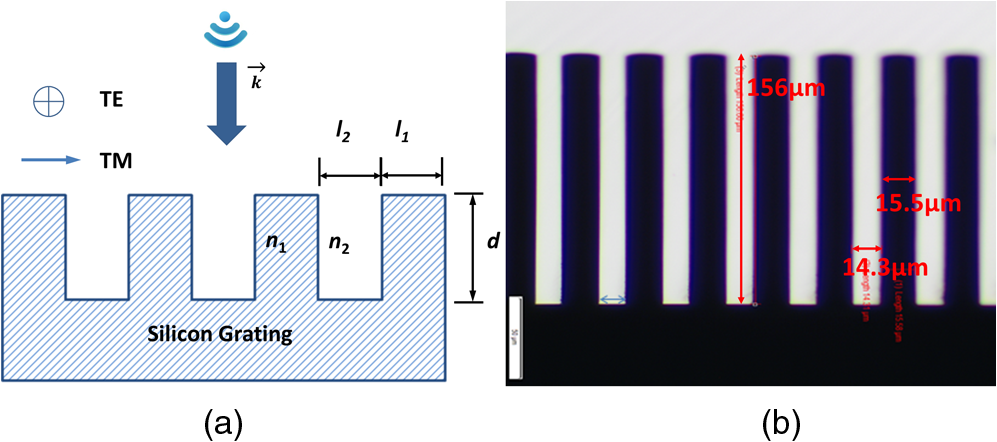
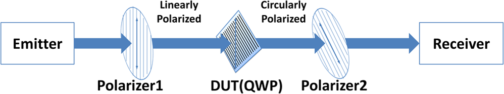
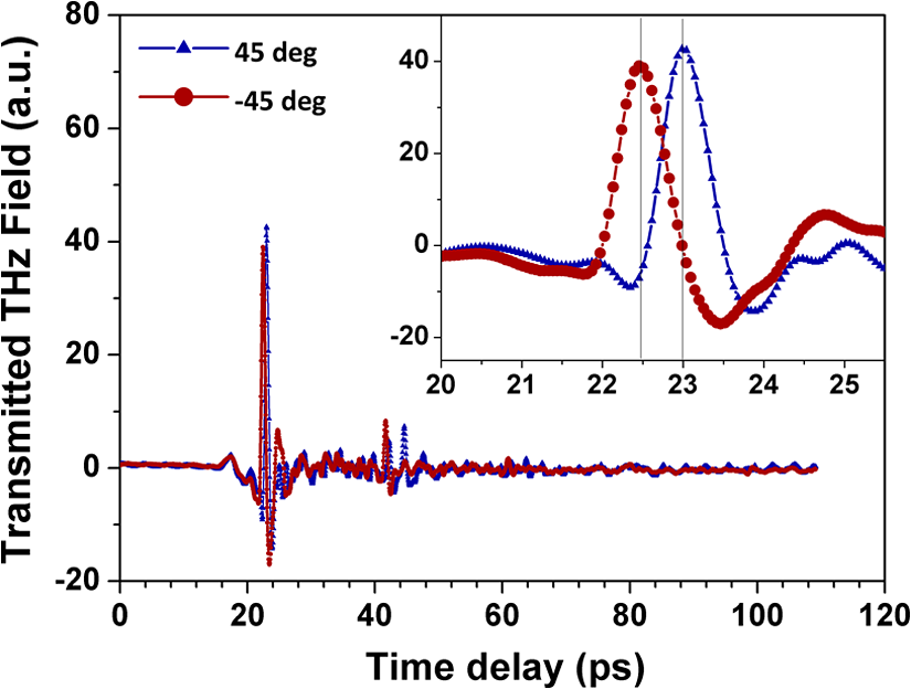
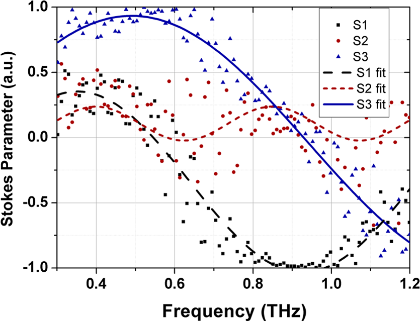
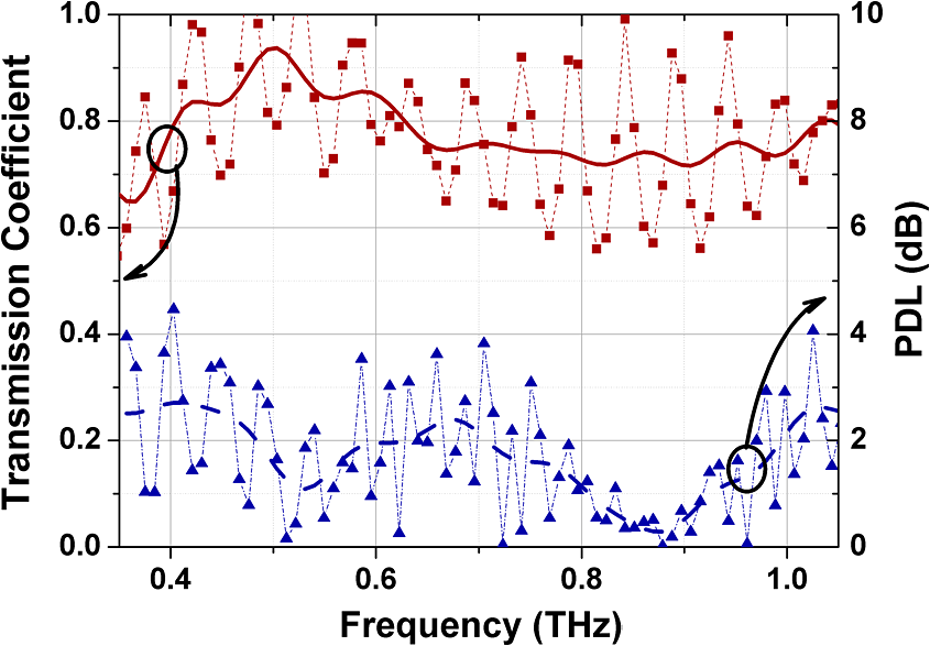
1.IntroductionAt present, terahertz technology has drawn significant attention due to its numerous applications in material inspection,1 semiconductor and medical imaging,2 security imaging, and communications.3 A variety of devices have been demonstrated and applied in real cases, including wave plates,4 filters,5 and phase shifters6 based on birefringence materials. Devices using form birefringence have a smaller size in comparison with natural birefringence materials, hence their being more suitable for integration.7 In this letter, we aim for developing a quarter-wave plate (QWP) using grating based on form birefringence structure operating in lower terahertz frequency range (0.51 THz in our work). Previous studies have demonstrated QWPs using various materials such as one-dimensional photonic crystals,7 stacked paper,8 polyethylene (HDPE),9 transparencies,10 and silicon wafers.11 However, most of the QWPs, especially those which operate at low frequency ranges, have relatively large sizes. In this letter, a thin QWP is presented with an operation frequency of 0.51 THz. The QWP is fabricated using a deep reactive ion etching (DRIE) technique to achieve a 156-μm-deep grating on a silicon substrate. Stokes parameters are utilized to characterize the QWP, which shows a good performance at 0.51 THz. The transmission coefficient and polarization dependent loss (PDL) are 0.93 and 1.4 dB at 0.51 THz, respectively. 2.Design and FabricationThe structure of QWP is shown in Fig. 1(a), where a grating on silicon substrate consists of alternating silicon and air components, with refractive indices and , and width and , respectively. A quasi-static effective medium theory (EMT) is utilized to describe the interaction between the micro grating structure and a THz wave, when the wavelength of the incident wave is much larger than the period of the grating.7 When the incident wave propagates along the direction , the grating exhibits effective birefringence, which is depicted as TE and TM in Fig. 1(a). The electrical fields transmit along the TE and TM directions with refractive indices given by where and are the fill factors of the silicon and air components respectively, and , . Our target operation frequency of the QWP is 0.5 THz, which corresponds to a wavelength of 600 μm. The grating period is set to 30 μm, which is much smaller than the wavelength, so that the quasi-static EMT is satisfied. Fill factors are set as . The refractive index of silicon is 3.415. The calculated effective refractive indices are , . The grating depth for a QWP at 0.5 THz is calculated as 130 μm.A 1-mm-thick, orientation , double side polished silicon wafer with resistivity larger than was used to fabricate a QWP described above. The wafer was coated with 1.2-μm-thick S1813 photo resist and soft baked at 100°C for 100 s. Then the wafer was exposed using a mask plate in a Suss MA8 aligner for 7 s at power and developed in MF-320 developer for 60 s. An MUC-21 (Surface Technology Systems) etching system was used in the DRIE process. The silicon wafer was etched in (200 SCCM, 10 s, 3 Pa) and (85 SCCM, 3 s, 2 Pa) cycling for 50 min. The coil and plate powers were 600 Watt and 15 Watt, respectively. In our preceding measurements, the calculation of the 130 μm grating was found to deviate a bit from the real result, due to the slightly inaccurate solution of the EMT.12 The etching depth was then optimized to 156 μm. Figure 1(b) shows the fabricated grating, where the widths of the silicon and air gap are 15.5 and 14.3 μm, respectively. 3.CharacterizationThe fabricated QWP is measured using our self-built polarimetric terahertz time domain spectroscopy system.13 As shown in Fig. 2, the incident THz beam is firstly linear polarized by polarizer 1, and then perpendicularly enters the QWP sample. Polarizer 2 acts as a polarization analyzer by rotating with different angles. The TE direction of the QWP sample is located at 45-deg with respect to the direction of polarizer 1. In this case, the incident wave is equally split into TE and TM components. After transmitting through the QWP, once the phase difference between TE and TM components equals to 90-deg, the output signal will become a circularly polarized beam. The time domain pulses are measured and shown in Fig. 3, when polarizer 2 is located at 45-deg (TE) and -45-deg (TM), respectively. The TE component is retarded 0.53 ps than TM component in Fig. 3. Fresnel reflection in the 1-mm-thick silicon substrate can also be observed as two small peaks separating from the main pulse by 21.6 and 19.3 ps for TE and TM components respectively. The QWP is also characterized using Stokes matrix.14 Figure 4 shows the calculated Stokes parameters, and corresponding fitting curves. The Stokes parameters (, , ) are close to (0, 0, 1) at around 0.5 THz, which means a circularly polarized beam as depicted in Fig. 2. The curve of is deviated a little from the ideal value of 0. This deviation possibly originates in the following reasons: the inherent noise of testing system, polarization dependent loss (PDL) of the QWP sample, and the angle deviation of exactly 45 deg. By our calculations, a Stokes parameter at 0.51 THz has the minimum variance 0.0015, with respect to (0, 0, 1). The small frequency deviation from 0.5 THz may be due to the variance in fabrication and scaling of the grating. The transmission coefficient of the QWP is measured and shown in Fig. 5, where the measured data is fitted using a finite impulse response (FIR) low pass filter. The silicon grating has a transmission coefficient larger than 0.6 in the range of 0.3 to 1 THz. The transmission coefficient at 0.51 THz is 0.8 in calculated data and 0.93 in fitting curve. The PDL is also calculated and shown in Fig. 5. A continuous curve fitting by FIR low pass filter shows less than 2 dB PDL in the overall range. The PDL is about 1.4 dB at 0.51 THz from fitting curve. Moreover, less loss can be achieved using silicon substrate with much higher resistivity, and an anti-reflection coating can also improve the transmission coefficient.11 4.ConclusionIn this letter, we designed and fabricated a thin quarter-wave plate operating at a lower terahertz frequency of 0.51 THz, with thickness of 156 μm, high transmission coefficient of 0.93 and low PDL of 1.4 dB at 0.51 THz. Less loss can be achieved using silicon substrate with much higher resistivity and anti-reflection coating. AcknowledgmentsThis work is supported by the international joint project between A-STAR of Singapore and JST of Japan with A-STAR/SERC/SICP grant No. 1021630069. The authors would like to thank Vincent Lim from IMRE A-STAR of Singapore for mask making. ReferencesK. Kawase,
“Terahertz imaging for drug detection and large-scale integrated circuit inspection,”
Opt. Photon. News, 15
(10), 34
–39
(2004). http://dx.doi.org/10.1364/OPN.15.10.000034 OPPHEL 1047-6938 Google Scholar
P. Y. HanG. C. ChoX.-C. Zhang,
“Time-domain transillumination of biological tissues with terahertz pulses,”
Opt. Lett., 25
(4), 242
–244
(2000). http://dx.doi.org/10.1364/OL.25.000242 OPLEDP 0146-9592 Google Scholar
R. Piesiewiczet al.,
“Performance analysis of future multi-gigabit wireless communication systems at THz frequencies with highly directive antennas in realistic indoor environments,”
IEEE J. Sel. Top. Quantum Electron., 14
(2), 421
–430
(2008). http://dx.doi.org/10.1109/JSTQE.2007.910984 IJSQEN 1077-260X Google Scholar
J.-B. MassonG. Gallot,
“Terahertz achromatic quarter-wave plate,”
Opt. Lett., 31
(2), 265
–267
(2006). http://dx.doi.org/10.1364/OL.31.000265 OPLEDP 0146-9592 Google Scholar
C.-Y. Chenet al.,
“Liquid-crystal-based terahertz tunable Lyot filter,”
Appl. Phys. Lett., 88
(10), 101
–107
(2006). http://dx.doi.org/10.1063/1.2181271 APPLAB 0003-6951 Google Scholar
C.-Y. Chenet al.,
“Room temperature terahertz phase shifter based on magnetically controlled birefringence in liquid crystals,”
Appl. Phys. Lett., 83
(22), 4497
(2003). http://dx.doi.org/10.1063/1.1631064 APPLAB 0003-6951 Google Scholar
M. SchellerC. JördensM. Koch,
“Terahertz form birefringence,”
Opt. Express, 18
(10), 10137
–10142
(2010). http://dx.doi.org/10.1364/OE.18.010137 OPEXFF 1094-4087 Google Scholar
B. Schergeret al.,
“Paper terahertz wave plates,”
Opt. Express, 19
(25), 24884
–24889
(2011). http://dx.doi.org/10.1364/OE.19.024884 OPEXFF 1094-4087 Google Scholar
S. C. Sahaet al.,
“Imprinted terahertz artificial dielectric quarter wave plates,”
Opt. Express, 18
(12), 12168
–12175
(2010). http://dx.doi.org/10.1364/OE.18.012168 OPEXFF 1094-4087 Google Scholar
Y. D. GongH. Dong,
“Terahertz waveplate made with transparency,”
in 37th Infrared, Millimeter, and Terahertz Waves (IRMMW-THz),
1
–2
(2012). Google Scholar
S. C. Sahaet al.,
“Low-loss terahertz artificial dielectric birefringent quarter-wave plates,”
IEEE Photon. Lett., 22
(2), 79
–81
(2010). http://dx.doi.org/10.1109/LPT.2009.2036242 IPTLEL 1041-1135 Google Scholar
I. Ritchteret al.,
“Design considerations of form birefringent microstructures,”
Appl. Opt., 34
(14), 2421
–2429
(1995). http://dx.doi.org/10.1364/AO.34.002421 APOPAI 0003-6935 Google Scholar
Y. D. GongH. DongP. Varghese,
“Simple methods to measure partial polarization parameters in the terahertz band using THz-TDS,”
Microw. Opt. Technol. Lett., 52
(9), 2005
–2007
(2010). http://dx.doi.org/10.1002/mop.v52:9 MOTLEO 0895-2477 Google Scholar
H. DongY. D. Gong,
“Measurement of Stokes parameters of terahertz radiation in terahertz time domain spectroscopy,”
Microw. Opt. Techn. Lett., 52
(10), 2319
–2324
(2010). http://dx.doi.org/10.1002/mop.v52:10 MOTLEO 0895-2477 Google Scholar
|