|
|
1.IntroductionFor some time the use of microelectromechanical systems and nanoelectromechanical systems (MEMS and NEMS)1 has opened the way for their application in several areas, ranging from biomedicine and communications to high-resolution measurement systems, including recent contributions that report the use of MEMS devices for mechanical energy harvesting.2,3 These devices, if combined and functionalized with electromagnetic resonant structures, serve for sensing,4–8 and energy recollection from electromagnetic waves.9 On the other hand, light can be used not only to excite or modulate the state of mechanical vibration but also to characterize the mechanical status and properties of these devices. In these situations, the relative phase between the vibrations of the cantilevers is of interest when combining the signals produced by individual cantilevers. On the other hand, when the components of the array are coupled one to each other, cooperative modes are possible and the method presented here can be applied to identify such modes, since it is sensitive to on-phase or counter-phase relative vibrations of some array components. Laser diffractometry is an optical technique well-suited for analyzing microstructures and has been successfully applied for the measurement of particle size distributions in several media.10 Diffractive imaging has been used in phase retrieval problems at various wavelength ranges. Most of the algorithms are based on the Gerchberg–Saxton method that iteratively relates two irradiance maps obtained at the plane of interest and also in the far field region.11–13 In the MEMS arena, optical methods are routinely used as the displacement detection mechanism,14–16 with the atomic force microscope probably the simplest and most well-known of these because it is based on the deflection of a light beam reflected by the cantilever itself.17 The analysis of the stationary status of cantilevers using diffraction has been used previously to understand the individual position of each cantilever.18,19 In our case we are interested in understanding the amplitude of the cantilever movement, and the mutual phase correlation between them. For a nonstationary, moving cantilever array, the frequency of the mechanical vibration cannot be followed by conventional image-acquisition systems. Therefore, the measured diffraction pattern is a temporal average of the instantaneous irradiance distribution. This fact makes it difficult to apply the previously reported methods and thus needs an alternative approach. When the vibration of a collection of microcantilevers has to be characterized, other specifically developed methods are able to efficiently detect the displacement of the collectivity of mechanical elements with high spatial resolution. This is accomplished by using an array of laser sources,20 or alternatively, by scanning a single laser beam across the full area of the array.21 However, because of the sequential nature of some of these methods they are unable to give a simultaneous picture of the dynamic state of all the array components and, consequently, no phase information of the vibration state can be detected. To overcome this drawback, in this paper we analyze the diffraction of the cantilever array. The diffraction pattern is registered and analyzed to identify the amplitude and vibration state of the array. We have compared the results from our simulation against those experimentally obtained from actual devices. The diffraction images have been analyzed to extract the desired parameters. As far as the diffraction pattern is formed collectively, and the registering method involves temporal average, the results obtained here may serve to better understand the effect of the coupling among cantilevers. This is one of the goals of this contribution: to obtain information about the phase relation related to the mutual coupling, using only the diffraction pattern produced by the array. The treatment presented here benefits from a simple model that uses a complex reflectivity window to resemble the reflectivity of the moving array of cantilevers. The modulus of this complex reflectivity is related to the actual reflectivity of the material of the cantilever, and the phase models show the actual change in shape of the cantilever. This approach is quite flexible and is able to include variations in frequency, vibrational modes, and mutual correlation among cantilevers. This paper is organized as follows. Section 2 describes the analysis of the MEMS system. In Sec. 3 we present the basic diffraction analysis of the array of cantilever. The treatment considers cantilever as a phase window whose diffraction pattern is properly calculated. Section 4 shows the experimental set-up used in the measurements. The experimental results are compared with the model output, and analyzed in more detail. Finally, Sec. 5 summarizes the main experimental and theoretical results of this contribution. 2.MEMS DeviceThe MEMS structure used in this paper was an array of nine silicon dioxide, , cantilevers. An optical image of this device is shown in Fig. 1. The cantilevers with dimensions length , width , and a thickness of 3.55 μm, are separated with a pitch . Fig. 1Optical image of the microelectromechanical systems (MEMS) device. The orientation of the coordinate system is also given.  As a previous step to the experimental measurements, several simulations in a Finite Element Method package (Comsol Multiphysics) were carried out in order to know the frequencies of resonance of the MEMS device. With these simulations we were able to find the values of the resonant frequencies for each mode as it is shown in Table 1. Table 1Resonance frequency of a SiO2 cantilever.
To excite the vibration of the mechanical structure we glued the sample on a piezoelectric actuator driven by a sinusoidal signal generator. The good solidification of the used glue makes the joint between the sample and the actuator mechanically reliable. The frequency of the generated signal was one of the resonance frequencies of the MEMS device. Several values for the signal amplitude were used. 3.Complex ReflectivityIn this section we show how the cantilever displacement produces a characteristic diffraction pattern that depends on the dimensions of the array and also on the actual geometric profile of its vibrational mode.22,23 After presenting the profile of the cantilever under study, we define a complex reflectivity to model phase variations produced by the cantilever vibration. Because of the simplicity of this method, it allows treating the whole array of cantilevers and even takes into account the mutual phase coupling amongst them. Also, it can be implemented easily in a simple and reliable algorithm. The profile of the displacement of the cantilever is given by the equation of a one-side clamped beam.1 This equation can be written in a normalized form as where is the length of the cantilever, is the coordinate along the cantilever length (see the orientation of the coordinate system given in Fig. 1), and the constant is given by with a mode constant that, for the geometry given here, has the following values for the first four vibrational modes (). This normalized profile is different for each mode (see Fig. 2). The actual amplitude of the vibration of the cantilever depends on the excitation voltage, , and the quality factor of the cantilever, . This provides a dimensional factor that is , where characterizes the piezo-electric actuator driving the cantilever. In our case , and . This value has been obtained by averaging the factors from each component of the array, where vibration frequency response has been characterized individually for each one. Thus, the displacement, , is given as . Therefore, the voltage driving the piezo actuator fixes the maximum amplitude of the vibration. In our experimental case, the maximum value of voltage, , produces a maximum amplitude at the tip of the actuator of . On the other hand we consider that the cantilever moves only as a function of , not showing dependence with the orthogonal coordinate . This means that is constant along the axis on the cantilever width.Fig. 2Normalized profiles of the vibration of a cantilever. The four plots correspond with the first four modes. These modes are characterized by a different value of the parameter in Eq. (1). 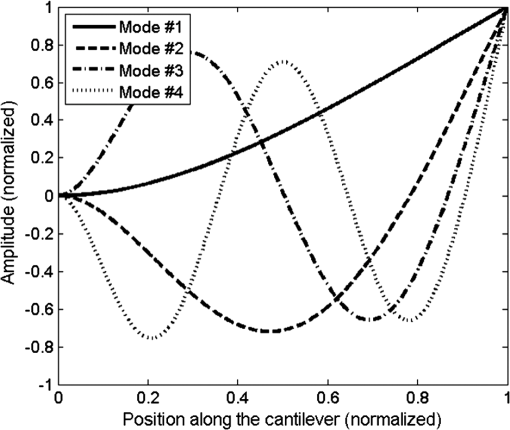 Once the profile of the vibration is obtained and analytically described, we now model the cantilever as a reflecting moving surface that will produce a diffraction pattern in the far field. We assume that this reflection can be modeled as a complex reflectivity where the modulus is related with the size and position of the cantilever arrangement and the phase is given by the vibrational state of each cantilever. This reflectivity can be expressed as where is the wavelength of illumination of the array. There is a factor 2 multiplying because the phase is produced in reflection mode and the displacement along has to be taken twice. This model is applicable because of the narrow range of displacement of the array with respect to its length. The function represents a map of the displacement of the cantilever arrangement. The domain of can be divided in subdomains corresponding to each one of the cantilevers. Each cantilever, labeled with a subindex , is represented by a function given by Eq. (1), , where the coordinates are applicable to the subdomain where the cantilever is located.By using Eq. (2) we can simulate any vibrational state and can model different phase situations of the cantilevers. In Eq. (2) we included the temporal evolution of the reflectivity. This time dependence can be given as a harmonic function at a frequency , related to the natural resonance of the cantilever, written as where represents a constant phase term. Both the frequency and the constant phase term can be different for each of the cantilevers in the arrangement. By using this method it is possible to simulate the differences between the frequencies of resonance of the cantilevers (variability in and ) and also their degree of mutual coupling (variability in ).Our goal is to obtain a computable solution for the far-field irradiance, , produced by the complex reflectivity characterizing the cantilever. If we assume a monochromatic plane wave illumination, the result is given as the Fourier transform of the complex reflectivity of the cantilever, , where and are the spatial frequencies associated with and , respectively. On the other hand, if the image is obtained with a charge-coupled device (CCD) camera, the vibrational frequency (see Table 1) is typically much larger than the frame rate of the camera. This fact produces a temporal averaging of the image. Therefore the retrieved image from the cantilever is expressed as where means the temporal averaging of the far-field pattern.4.Experimental ResultsIn this section we first present the experimental set-up used to register the diffraction pattern of the vibrating array of cantilevers. Then, the experimental results are described and compared with those obtained from the analytical model. The diffraction pattern produced by the cantilever is obtained by means of an optical set-up pictured in Fig. 3. This figure represents the set-up used to remove undesired diffraction patterns caused by the metallic areas surrounding the cantilever. The illuminated beam, cantilever location and screen are placed to show a large angle of incidence. The light source is an He-Ne laser set at 632.8 nm, with the size of the beam at the cantilever locations large enough to fill the array with a uniform illumination. The actual angle of incidence used in the experiments reported in this paper is 20 deg. The cantilevers are mounted on a positioning stage and the generated pattern is then projected onto a screen placed at a distance ranging from 0.5 to 2.5 m within the Fraunhofer diffraction regime, and showing a Fresnel number lower than 0.025 for the experimental situations treated in this paper. The orientation of the coordinate system is shown in the bottom left corner of Fig. 3. The plane is the plane of incidence. The inset in Fig. 3 shows an image obtained with this arrangement and a diffraction pattern produced both by the cantilever array and also by the reflective portion of the cantilever located at the clamped side. This artifact can be eliminated by placing a blocking element that avoids the illumination of the stationary part of the device. Figure 4 presents the diffraction patterns obtained before (a), and after (b) removing the undesirable stationary diffraction pattern. Figure 4(b) shows a well-resolved diffraction pattern. The distance between the main diffraction maxima is about 1 cm when the screen is placed at 2.5 m from the array. The secondary maxima located between the observed maxima can be also resolved by the registering system. Alternatively, the diffraction pattern can be directly captured using a CCD camera placed at shorter distance from the cantilevers than the projection screen and looking towards the cantilevers. Both methods of registering the diffraction pattern produce the same structure. Fig. 3Image of the measurement set-up showing the location of the cantilever and the screen. This set-up was used when removing the spurious diffraction pattern caused by the structures around the cantilevers. The inset of this image shows the diffraction pattern observed on the screen. In the bottom-left part we show the orientation of the coordinate system along with the illumination and observation directions that lie on the plane. 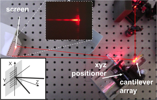 Fig. 4Diffraction patterns of the array of cantilevers registered before removing the stationary part (a) and after blocking the illumination on this portion of the array (b).  After adjusting the angular parameters of the incidence to optimize the capture of the diffraction pattern, the cantilevers are piezo-electrically excited with an external voltage signal. The images obtained with this arrangement are shown in Fig. 5 for three values of the driving voltage (0.0, 0.5, and 1.0 V). These images have been treated to remove some artifacts appearing during acquisition. Actually, the image at the left of this figure corresponds with the stationary case (driving voltage at 0 V). This case should be taken as a reference in order to evaluate the displacement of the cantilevers. We may see that the horizontal extension of the maxima increases as voltage increases. Also the distribution of light along these horizontal maxima is moving towards the outer parts of the pattern when voltage is larger. On the other hand, even for 0.0 V driving voltage, there is a nonnegligible contribution to the diffraction pattern coming from diffuse reflection on the cantilever. This diffuse reflection contribution reduces the contrast of the diffraction pattern and masks the location of the secondary maxima and minima. Fig. 5Time-averaged diffraction patterns as a function of the supplied voltage to the piezoelectric.  To validate the model given in Sec. 3, we have taken the experimental images shown in Fig. 5 and extracted two perpendicular profiles along the horizontal (-axis) and vertical (-axis) directions intersecting at zero. In order to reduce the noise in these profiles we averaged the image, taking 20 columns for the vertical profile, and 10 columns for the horizontal profile. For our experimental set-up the angular subtend of each pixel is 0.00072 deg in each direction. The next step has been to evaluate the profile obtained from the simulation of a variety of cases. The parameters for these variations are the excitation voltage of the cantilever, the vibration mode, and the correlation among the vibration of each individual cantilever. The excitation voltage is linked with the quality factor of the cantilever set. The correlation is mostly described by taking into account the relation between the individual phases of the vibration of the cantilevers. A total correlation would mean that ; we labeled this case as CTN (ConsTaNt). A more realistic case should take into account a partial correlation among the individual phases. This correlation is caused by the mechanical constraint produced by the common metallic portion at the clamped side of the cantilever. We have considered two cases. For the case labeled as RNB (RaNdom Bounded) the phase varies randomly but restricted, or bounded, to the interval [0 deg, 100 deg]. The second case, named as RND (RaNdoM), allows a random value for the phase of each cantilever along the whole 360-deg range. The first case (first row of Fig. 6) is for an excitation of 0 V. However, we cannot be assured that the cantilevers are in the same plane. We assume that the cantilevers are at rest but flexured at different positions following the profile given by vibration mode Number 1. We modeled this case as that obtained for a small excitation (0.1 mV) having an RND phase distribution. When comparing this case with the 0 V, having all the cantilevers flat and at rest (dashed line in the first row of Fig. 6), we may check that the RND case is fitting better in the registered diffraction pattern. Fig. 6Vertical (a) and horizontal (b) profiles of the far-field diffraction pattern obtained from the experimental set-up compared with the simulated results. The rows correspond to different driving voltages: 0 V (first row), 0.5 V (second row), and 1 V (third row). The gray dots are for the experimental values, and the solid and dashed lines correspond with different mode oscillation (Nos. 1 and 2), and different phase correlations. RND means an unbounded random phase correlations, CTN means total phase correlation, and RNB applies to a bounded random phase difference between cantilevers. 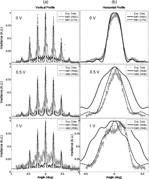 When the voltage increases, the cantilevers begin to oscillate. The method explained previously produces simulated profiles for a wide variety of cases. The main parameters are the excitation voltage, the vibration mode under analysis, and the initial phase correlation among cantilevers. In the second and third row of Fig. 6 we plotted the results obtained from the simulation for two cases that fit with the experimental result. These correspond with a bounded random variation of the initial phases (RNB) and oscillating in the first and second modes. We may see that although the fitting is about the same for both modes along the vertical direction, the experimental horizontal profile fits better with an oscillation of the second mode. At this point it is important to note that the far-field diffraction pattern describes a collective contribution of the whole array of cantilevers. We cannot follow the individual behavior of each cantilever with this method. However, we can still infer the vibration mode and the phase correlation between cantilevers. 5.ConclusionsIn this paper, we presented an analytical model describing the diffraction pattern of a collection of vibrating cantileves. The model is based on the definition of a complex reflectivity that corresponds with the two-dimensional (2-D) geometry of the actual cantilevers. Besides, if necessary, the complex reflectivity could introduce individual variations in shape, size, or material for each cantilever, adding the effect of the reflective surrounding structures. This makes this method quite flexible and applicable to a wide variety of cases involving stationary or vibrating cantilevers. This approach takes into account vibrational modes, driving voltages, varying frequencies of vibration, and arbitrary phase relations among the individual vibrations of an array of cantilevers. The temporal period associated with the vibration of the cantilevers is much larger than the integration time of image-registering equipment. Therefore, the diffraction patterns are temporal averages, over a large number of vibration periods of the movement of the cantilevers. The results of the model were checked using the diffraction patterns obtained from an experimental set-up. To obtain the images, the cantilevers reflect light onto a registering media located within the Fraunhofer diffraction region. The experimental results show a good agreement with the simulated images obtained from the model itself. Actually, by comparing the experimental results with the analytical ones we can identify the vibrational mode of the device and the initial phase relations appearing along the array of cantilevers. The method proposed here can be generalized to deal with a variety of cantilever geometries and only needs to register far-field diffraction images obtained by reflection from the cantilever array. AcknowledgmentsThis work has been supported by project ENE2009-14340 from the Spanish Ministry of Science and Innovation. ReferencesG. M. Rebeiz, RF MEMS: Theory, Design and Technology, John Wiley & Sons, New Jersey
(2003). Google Scholar
Y. QinX. WangZ. L. Wang,
“Microfibre-nanowire hybrid structure for energy scavenging,”
Nature, 451
(7180), 809
–813
(2008). http://dx.doi.org/10.1038/nature06601 NATUAS 0028-0836 Google Scholar
G. Murilloet al.,
“Harvester-onchip: design of a proof of concept prototype,”
Microelectron. Eng., 86
(4–6), 1183
–1186
(2009). http://dx.doi.org/10.1016/j.mee.2009.01.081 MIENEF 0167-9317 Google Scholar
K. L. EkinciY. T. YangM. L. Roukes,
“Ultimate limits to inertial mass sensing based upon nanoelectromechanical systems,”
J. Appl. Phys., 95
(5), 2682
–2689
(2004). http://dx.doi.org/10.1063/1.1642738 JAPIAU 0021-8979 Google Scholar
M. Gritzet al.,
“Fabrication of air bridges using electron beam lithography,”
J. Vac. Sci. Technol. B, 21
(1), 332
–334
(2003). http://dx.doi.org/10.1116/1.1539062 JVTBD9 0734-211X Google Scholar
M. E. Motamedi, MOEMS: Micro-Opto-Electro-Mechanical Systems, SPIE Press, Bellingham, WA
(2005). Google Scholar
J. Aldaet al.,
“Optical antennas for nanophotonic applications,”
Nanotechnology, 16
(5), S230
–S234
(2005). http://dx.doi.org/10.1088/0957-4484/16/5/017 NNOTER 0957-4484 Google Scholar
K. Jensenet al.,
“Nanotube radio,”
Nano Lett., 8
(1), 374
–374
(2008). http://dx.doi.org/10.1021/nl073089g NALEFD 1530-6984 Google Scholar
D. Okawaet al.,
“Surface tension mediated conversion of light to work,”
J. Am. Chem. Soc., 131
(15), 5396
–5398
(2009). http://dx.doi.org/10.1021/ja900130n JACSAT 0002-7863 Google Scholar
L. Beuselincket al.,
“Grain-size analysis by laser diffractometry: comparison with the sieve-pipette method,”
CATENA, 32
(3–4), 193
–208
(1998). http://dx.doi.org/10.1016/S0341-8162(98)00051-4 CIJPD3 0341-8162 Google Scholar
R. W. GerchbergW. O. Saxton,
“A practical algorithm for the determination of phase from image and diffraction plane pictures,”
Optik, 35
(2), 237
–246
(1972). OTIKAJ 0030-4026 Google Scholar
H. M. Quineyet al.,
“Diffractive imaging of hihgly foculsed X-ray fields,”
Nat. Phys., 2
(2), 101
–104
(2006). http://dx.doi.org/10.1038/nphys218 NPAHAX 1745-2473 Google Scholar
W. ChenX. Chen,
“Quantitative phase retrieval of complex-valued specimens based on noninterferometric imaging,”
Appl. Opt., 50
(14), 2008
–2014
(2011). http://dx.doi.org/10.1364/AO.50.002008 APOPAI 0003-6935 Google Scholar
D. KarabacakT. KouchK. L. Ekinci,
“Analysis of optical interferometric displacement detection in nanoelectromechanical systems,”
J. Appl. Phys., 98
(12), 124309
(2005). http://dx.doi.org/10.1063/1.2148630 JAPIAU 0021-8979 Google Scholar
D. Karabacaket al.,
“Optical knife-edge technique for nanomechanical displacement detection,”
Appl. Phys. Lett., 88
(19), 193122
(2006). http://dx.doi.org/10.1063/1.2203513 APPLAB 0003-6951 Google Scholar
J. Agustíet al.,
“Optical vibrometer for mechanical properties characterization of silicalite-only cantilever based sensors,”
Microelectron. Eng., 87
(5–8), 1207
–1209
(2010). http://dx.doi.org/10.1016/j.mee.2009.12.009 MIENEF 0167-9317 Google Scholar
J. E. SaderJ. W. M. ChonP. Mulvaney,
“Calibration of rectangular atomic force microscope cantilevers,”
Rev. Sci. Instrum., 70
(10), 3967
–3969
(1999). http://dx.doi.org/10.1063/1.1150021 RSINAK 0034-6748 Google Scholar
O. Pjetriet al.,
“Using diffraction to detect deflection of the cantilevers in an array,”
in Micromechanics and Microsystems Technology Europe Workshop,
(2011). Google Scholar
J. W. van Honschotenet al.,
“Information storage and retrieval for probe storage using optical diffraction patterns,”
J. Appl. Phys., 110
(10), 104309
(2011). http://dx.doi.org/10.1063/1.3657945 JAPIAU 0021-8979 Google Scholar
H. P. Langet al.,
“Sequential position readout from arrays of micromechanical cantilever sensors,”
Appl. Phys. Lett., 72
(3), 383
–385
(1998). http://dx.doi.org/10.1063/1.120749 APPLAB 0003-6951 Google Scholar
N. F. Martínezet al.,
“High throughput optical readout of dense arrays of nanomechanical systems for sensing applications,”
Rev. Sci. Instrum., 81
(12), 125109
(2010). http://dx.doi.org/10.1063/1.3525090 RSINAK 0034-6748 Google Scholar
E. Hecht, Optics, 4th ed.Addison Wesley, San Francisco
(2001). Google Scholar
J. W. Goodman, Introduction to Fourier Optics, 3rd ed.Roberts & Company, Englewood, Colorado
(2004). Google Scholar
Biography Alexander Cuadrado obtained a BS in electronic engineering from the University of Basque Country in Bilbao, Spain, in 2010 and an MS in photonics from the Universidad Autónoma de Madrid, Madrid, Spain in 2011. Currently he is working on his PhD at the University Complutense of Madrid, Madrid, Spain, in the Applied Optics Complutense Group, where he is researching the electromagnetic and thermal response of nanophotonic structures, focusing on the analysis of optical antennas, and in the characterization of MEMS devices that incorporate electromagnetically resonant elements.  Jordi Agustí received his BS in telecommunications in 2007, and his MS in electronic engineering in 2009 from the Universitat Autònoma de Barcelona, Barcelona, Spain, where he is currently working toward his PhD in the Electronic Engineering Department. His research interests include design, characterization, and integration of MEMS and NEMS, especially to harvest energy from electromagnetic radiation.  Gabriel Abadal has been an associate professor of electronics at the Electronics Engineering Department of Universitat Autònoma de Barcelona since 2002. Since his postdoctoral stay with Nanotech-DTU (Denmark) in 1998, he has researched resonant electrically excited cantilevers and cantilever-based sensors and introduced the development of MEMS and NEMS in his department at UAB. He has also developed departmental investigations related to the development, integration, and characterization of MEMS, NEMS and MEMS-CMOS. Since 2006, he has focused his activity in the application of MOEMS and NOEMS in energy-harvesting from ambient vibrations and from new energy sources at the nanoscale.  Javier Alda graduated as a Licenciado in Sciences from the University of Zaragoza and received a PhD in physics from the University Complutense of Madrid, Madrid, Spain. He joined the Optics Department of the University Complutense of Madrid in 1985, where he currently is professor of optics. He has coauthored more than 100 papers and book chapters and communications to international meetings and conferences. He holds three patents in optics and has been a visiting researcher at the University of Central Florida, Stanford University, and Universidad Autónoma de San Luis Potosí. His main research interest is in applied optics, with special emphasis in the analysis and characterization of optical antennas and resonant optics. He is a member of the International Society for Optical Engineering, the European Optical Society, and the Optical Society of America. |

