|
|
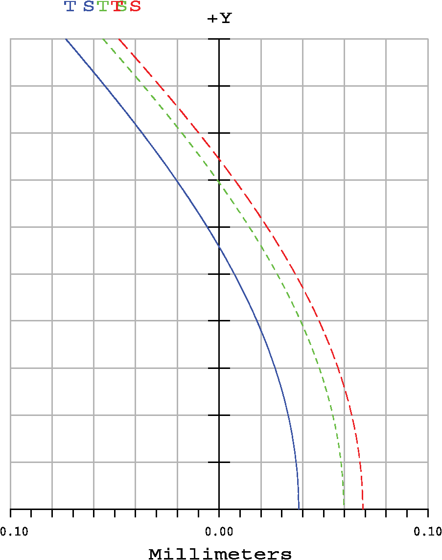
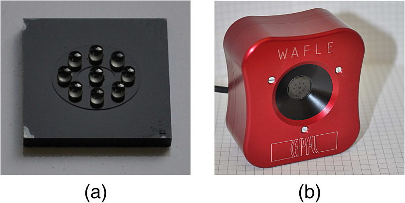
1.IntroductionThe camera objective is the most difficult element to integrate into nomadic devices. In addition to the significant thickness of the objective, its mounting requirements are often difficult to meet and are costly. These problems stem from the traditional approach to control the aberrations using a series of lenses placed sequentially along the optical axis.1 Novel approaches include the use of the wavefront coding method to simplify the lens systems2,3 and multichannel objectives.4–11 For fabrication and integration advantages, the multichannel objectives are made very thin using small optical channels. However, the angular resolution of these systems is limited and superresolution techniques, such as the thin observation module by bound optics method,5 are required.10–12 Multichannel systems offer many design possibilities, each obtained by weighting differently the numerous design constraints. In our work,13 we aim at a system with two main properties: the optics has to be simple for easy fabrication using wafer-level mass production14–16 and its size has to be adequate to potentially achieve good angular resolution without resorting to superresolution techniques. We opted for a simple plano-convex design with lenses having a diameter of 1.0 mm. The size of the different fields and the number of channels were selected from the quality of the areal image. In contrast to existing realizations,11,17 the field curvature was corrected by the axial position of the channel optics. The result is the design of a multichannel system having only a few channels. Details of the design, of the fabrication method, and of the preliminary optical characterization are given in this paper. 2.Optical DesignThe image produced by a single-lens system lies on a curved surface. This aberration is called field curvature. It cannot be reduced in a single-lens system. The effect of a curved field could be avoided by using an identically curved image sensor.18,19 Unfortunately, these sensors are not yet commercially available. Within the multichannel framework, the curvature of the field can be accommodated for by changing the optical power of each channel. This approach was demonstrated using elliptical micro lenses of varying radii of curvature.17 As it is technically challenging to produce an array of lenses of different power, we propose to use lenses of identical power located at different distances from the sensor as depicted in Fig. 1. On the left side, three lens systems are drawn. These systems form three separated images on a flat image sensor represented by the vertical line. Each lens is located at a different axial position and the corresponding curved fields cross the sensor at different heights. The part of the field that appears sharp on the sensor depends on the depth of field. It is represented by a continuous line. On the right, the three fields are sketched. For each system, the hatched area represents the sharply imaged part of the field. Fig. 1Drawing of three-lens systems forming three images on a flat sensor represented by a vertical continuous line (center). The three lenses are identical. They form sharp images over a curved field (dashed line). Each lens is located at a different axial position and its curved field crosses the sensor at a different height. On the right, the three fields are represented. The hatched areas indicate the field areas sharply imaged on the sensor.  2.1.Plano-Convex ObjectiveA plano-convex lens has a small number of free parameters. For a given material, the desired lens power sets the radius of curvature of the convex surface. The remaining free parameters are the lens thickness and the size of the aperture stop and its position. By locating the aperture stop at the plane surface of the lens and by setting the thickness of the lens equal to the radius of curvature of the convex surface, as shown in Fig. 2, the lens is free from primary coma, astigmatism, and lateral chromatic aberration.20 For this stop position, the amount of both distortion and field curvature is large. The image distortion can be corrected digitally,21 but the effect of field curvature has to be corrected optically. Here we use the multichannel concept as shown in Fig. 1. The remaining first-order aberrations are the spherical aberration and the longitudinal chromatic aberration. For the lens dimension considered, spherical aberration has a stronger effect than longitudinal chromatic aberration. It can be reduced using an aspheric lens profile or by reducing the aperture of the stop. Fig. 2Schematic drawing of the thick plano-convex lens with the aperture stop at the plane surface, a design close to the rear landscape lens,22 but with a single curved surface. The arrow indicates that the centre of curvature of the convex surface is at the centre of the aperture.  State-of-the-art facilities can fabricate lenses with a diameter of 1.0 mm and more at the wafer level. In the Ecole Polytechnique Fédérale de Lausanne–Optics and Photonics Technology research facilities, however, this is currently not possible. Therefore, we rely on commercially available spherical lenses (45223, Edmund Optics, USA) having a diameter of 1.0 mm and a focal length of 1.0 mm. The optical design is tailored to a color webcam sensor (C600, Logitech, Switzerland) having square pixels with a side length of 2.835 μm. The sensing area is . It is covered by a Bayer filter and a glass window. We set the acceptable blur diameter , a value close to the length of 4 pixels. Using a ray tracing software or geometrical optics calculations,20,23 the maximum acceptable radius of the stop can be determined. That limit is reached when the image blur due to spherical aberration is equal to the acceptable blur . We found a radius of 0.166 mm giving an -number of 3. The depth of focus of this lens system is 60 μm. Using a ray tracing software (Radiant Zemax, USA), we generated the plots of field curvature shown in Fig. 3 for a field angle up to 40 deg and for three wavelengths—486, 589, and 656 nm. The axial displacement between the blue (continuous) and the red (long-dash) curves reveals a maximum longitudinal chromatic aberration of 30 μm on axis, a value much smaller than the depth of focus. Therefore, the effect of longitudinal chromatic aberration on the image quality is expected to be small. However, the maximum focus shift, which is due to field curvature, is 115 μm, a value twice as large as the approximated depth of focus. This aberration seriously degrades the image quality. Using two-lens systems (channels) axially shifted by 60 μm, a sharp image of the total field can be acquired. 2.2.System Layout and Field Curvature CorrectionThe optical system we designed consists of a central plano-convex lens that images a field of and satellite channels that extend the field to 40 deg. For a good use of the sensor area, the field extension is divided into eight annular sectors of 45 deg and arranged as depicted in Fig. 4(a). In that drawing, the circles represent the position of the channel apertures, the rectangle represents the sensor area, and the blue areas represent the useful parts of the image from each channel. Fig. 4(a) Schematic drawing of the field layout, the circles represent the position of the aperture stops, the rectangle represents the sensor area, and the blue (filled) zones represent the field image from each channel. (b) Cross-section drawing of the designed optical system passing through the center lens (top) and the satellite lenses (bottom). The 1.1-mm-thick wafer support posts of different thickness onto which the lenses are glued. The front surface of the wafer (B) is covered with black photoresist with aperture used to separate the different fields. The back surface (A) is also covered with black photoresist with aperture defining the channel stops. The sensing surface is on the right (S). Rays from three different field angles, 0, 27, and 40 deg, are traced for both channels (blue). 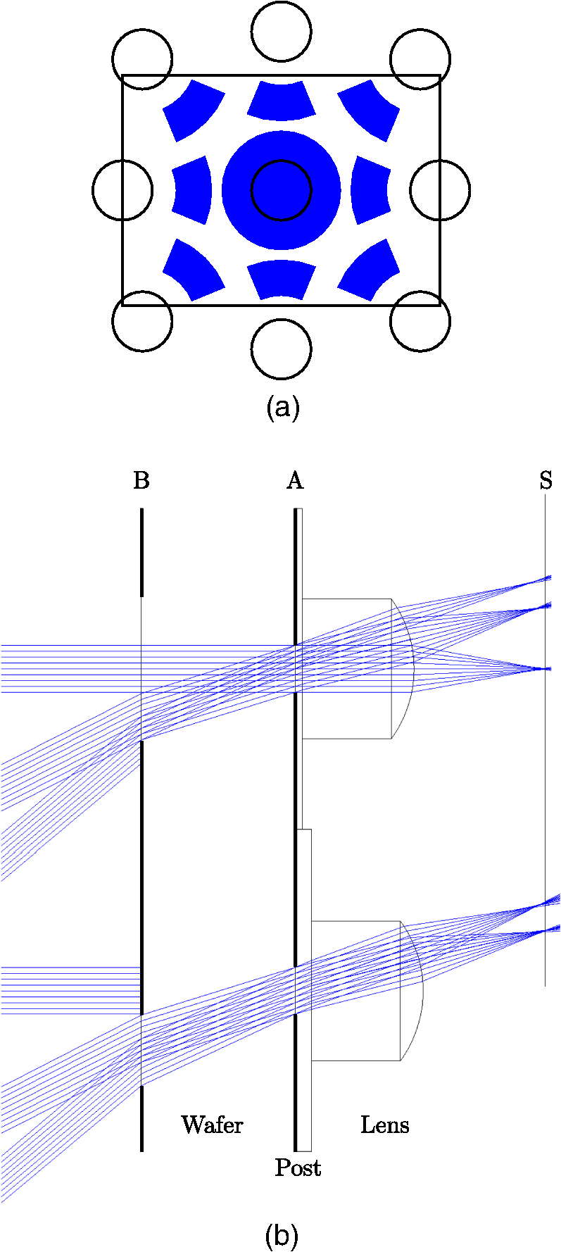 A cross-sectional view of the central channel and of one of the satellite channels is shown in Fig. 4(b). Apertures are formed on both sides of a glass wafer. On the back side (A), we have the aperture stops. On the front side (B), limiting apertures are used to avoid light cross-talk between the different channels. The lenses are glued on the back side. The satellite lenses are on a post used to compensate the field curvature. On the right, the image sensor (S) is represented. The designed total track length is 3.0 mm. 3.FabricationThe multichannel objective is fabricated using circular glass wafers with a diameter of 4 in. and with a thickness of 1.1 mm (D263T, Schott, Germany). On a single wafer, 16 square modules with a side length of 11 mm are fabricated in parallel. The two sides of the wafer were covered by black photoresist (EK410, Everlight Chemical Industrial Co., Taiwan). Photolithographic steps are used to form apertures on both sides. On the back side of the wafer, the aperture stops with a diameter of 0.33 mm are formed. On the front side, limiting apertures are formed to avoid light cross-talk between the different channels. The posts on the back side of the wafer were fabricated by replication in a layer of glue (NOA83H, Norland Products Inc., USA). The mould was fabricated in two steps. First, a 60-μm-thick layer of photoresist was patterned photolithographically to obtain the desired shape. Then, this pattern was transferred into a polydimethylsiloxane (PDMS) stamp. Finally, the nine lenses were aligned relative to the aperture stops and they were glued. The alignment procedure was done under microscopic observation using two micromanipulators. A photograph of the multichannel objective is shown in Fig. 5(a). We measured the lens centering relative to each aperture stop and we found an average shift of 13 μm. The multichannel objective is then glued on a circular support. It is aligned in front of the camera and enclosed into a dedicated box as seen in Fig. 5(b). 4.Experimental ResultsFigure 6 shows an image of a square grid superimposed with marks delimiting the field to be imaged by each channel. The inner circle extends to a field angle of 27 deg and the outer circle to 40 deg. The central image is sharp up to a field angle of 27 deg. For larger field angle, the image sharpness and contrast decrease. Each satellite channel images its dedicated field sharply and without vignetting. Fig. 6Raw image of a grid acquired with the multichannel objective. The central circle extends to a field angle of 27 deg and the external one to 40 deg. The central image is sharp up to about 27 deg. The satellite images are sharp between 27 and 40 deg as designed. The numbers 1 to 3 indicate the location of the modulation transfer function (MTF) measurements shown in Fig. 7. 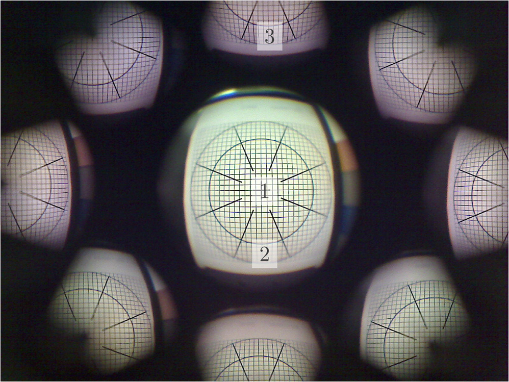 The effect of the field curvature correction is directly visible in Fig. 6. However, to quantify the improved image quality, we measured the modulation transfer function (MTF) at the three locations shown in Fig. 6: (1) in the center of the image of the central channel, (2) at a field angle of 33 deg on the image of the central channel (at 6 h), and (3) at a field angle of 33 deg on the image of the corresponding satellite channel (top). We used the slanted edge method24,25 to avoid aliasing due to the low sampling resolution of the camera. The MTF curve for the three image locations are shown in Fig. 7. The MTF curve for the field angle of 33 deg of the central channel image (2) is lower than the other two curves. It reaches a modulation of 0.3 for a spatial frequency of . For the other two curves, that is for the central location (1) and for the corrected satellite image (3), a modulation better than 0.3 is obtained up to a spatial frequency of . These results are in close agreement with the MTF obtained from ray tracing. The standard deviation obtained from 10 repeated measurements is smaller than 0.05. Fig. 7Measured MTF plot for the three image locations shown in Fig. 6. The location (1) is in the center and (2) at a field angle of 33 deg of the central channel image. The location (3) is in the satellite image corresponding to the location (2). The continuous (S1) and dashed (S2) lines represent the simulated MTF for the positions (1) and (2), respectively. 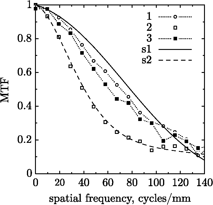 For image reconstruction, the four corners of the annular sectors were used as landmarks in a linear, two-dimensional mapping routine using Matlab® (The Mathworks Inc., USA). Figure 8(a) shows the raw image of the grid from the central channel as in Fig. 6. Figure 8(b) shows the digitally reconstructed image. The mapped area in the reconstructed image is clearly visible due to uncorrected brightness and color variations from the raw image. These effects, as well as the strong barrel distortion, can be corrected digitally.26 In this close-up view, the improved image sharpness in each 45-deg sector is clearly visible. Fig. 8(a) Raw image of the central channel from Fig. 6. (b) Reconstructed image obtained by mapping the images of the satellite channels. 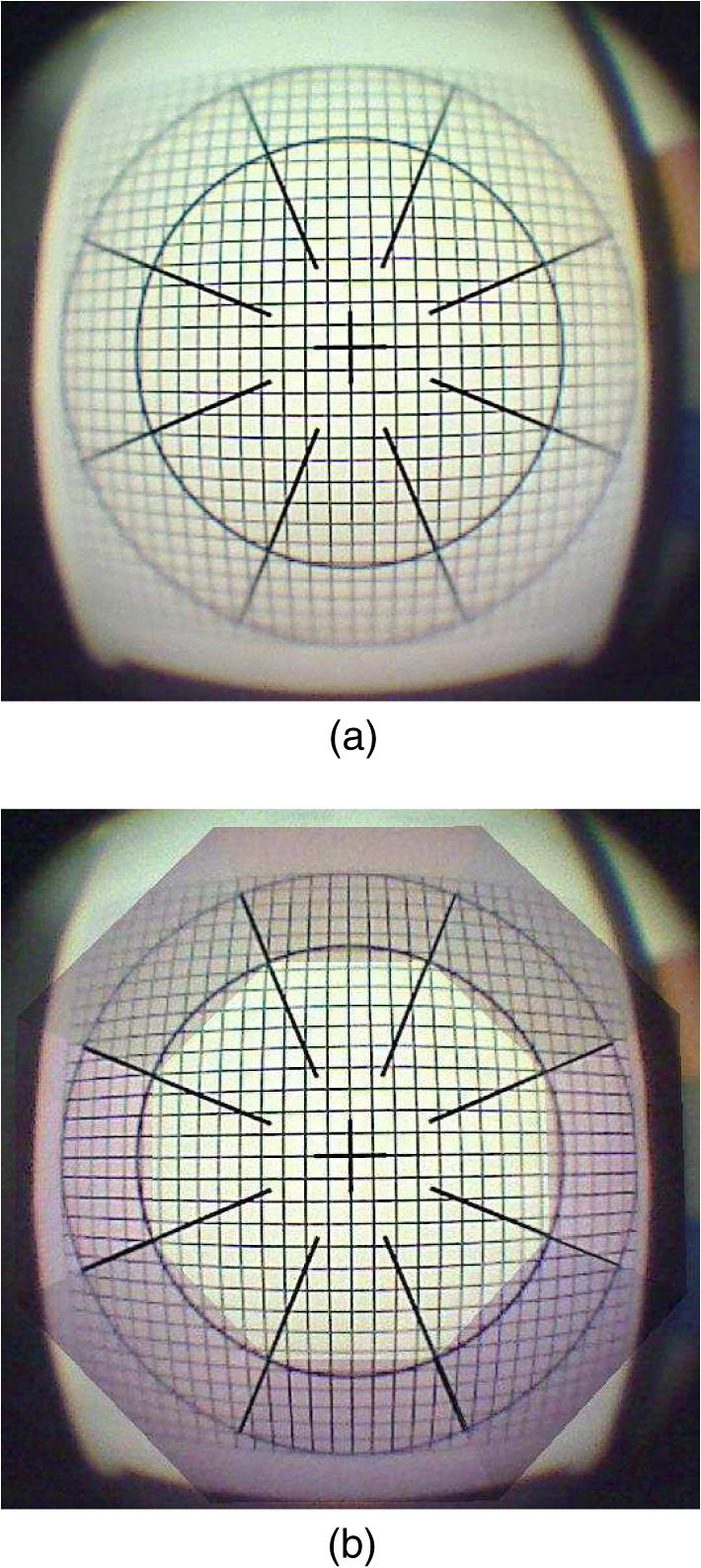 The reconstruction mapping obtained using the grid image is now used to reconstruct the images acquired with the multichannel objective. Figure 9 shows the image of a few books. The writings on the mapped area are easier to read in the corrected image than in the original image. 5.ConclusionWe have designed and fabricated a multichannel imaging system using plano-convex lenses on a single wafer. Nine separated channels image different parts of the field of view. The field curvature is corrected piecewise for the first time by axially positioning the optics of each channel. The field curvature correction was measured. Reconstructed images were obtained using simple image mapping. Digital processing of the images is required to assemble the full-field image from the subfield images. In addition, the image distortion, the color balance, and the image brightness should be corrected.26 All these operations can be integrated into the embedded electronic of current image sensors. Although a manual intervention was required to glue the lenses, our multichannel objective can be replicated using moulding technology. Furthermore, in state-of-the-art facilities, lenses of the required dimension can be fabricated at the wafer level using the reflow technique,14,15 enabling cheap production. The objective presented here can be improved further. For example, the primary spherical aberration could be corrected by an aspheric surface at the aperture stop. The angular resolution would be significantly improved, leading to large changes in the design. Indeed, the sampling would have to be adapted using an image sensor with smaller pixels. The acceptable blur size will decrease, resulting in a shallower depth of field. And the number of channels required to cover the same field of view will greatly increase. Another improvement can be achieved using an all wafer-level design. By placing the aperture stop on the front side, using the thickness of the wafer to form the lens body, and moving the vignetting aperture to the back side, the thickness of the objective can be reduced from the current 3 mm down to 1.9 mm, keeping the focal length of 1 mm. Other possible improvements include an optimization of channel cross-talk suppression, which will lead to a better usage of the sensing area, the correction of the image brightness (-law), the use of superresolution technique, and of a state-of-the-art image sensor. The objective presented here is an example of a multichannel objective. It illustrates the large variety of designs that can be reached by varying the weight put on different parameters. We hope it will stimulate further research in this field. AcknowledgmentsThe authors wish to thank Irène Philipoussis Fernandez for her technical expertise and Durgesh Kumar for his help with the digital image reconstruction. This work was supported by the Eurostars project 4303 WAFLE. ReferencesW. J. Smith, Modern Lens Design: A Resource Manual, 1st ed.McGraw-Hill, New York
(1992). Google Scholar
E. R. Dowski Jr.W. T. Cathey,
“Extended depth of field through wave-front coding,”
Appl. Opt., 34
(11), 1859
–1866
(1995). http://dx.doi.org/10.1364/AO.34.001859 APOPAI 0003-6935 Google Scholar
W. T. CatheyE. R. Dowski,
“New paradigm for imaging systems,”
Appl. Opt., 41
(29), 6080
–6092
(2002). http://dx.doi.org/10.1364/AO.41.006080 APOPAI 0003-6935 Google Scholar
K. HamanakaH. Koshi,
“An artificial compound eye using a microlens array and its application to scale-invariant processing,”
Opt. Rev., 3
(4), 264
–268
(1996). http://dx.doi.org/10.1007/s10043-996-0264-6 1340-6000 Google Scholar
J. Tanidaet al.,
“Thin observation module by bound optics (TOMBO): concept and experimental verification,”
Appl. Opt., 40
(11), 1806
–1813
(2001). http://dx.doi.org/10.1364/AO.40.001806 APOPAI 0003-6935 Google Scholar
K.-H. JeongJ. KimL. P. Lee,
“Biologically inspired artificial compound eye,”
Science, 312
(5773), 557
–561
(2006). http://dx.doi.org/10.1126/science.1123053 SCIEAS 0036-8075 Google Scholar
G. Druartet al.,
“Demonstration of an infrared microcamera inspired by Xenos Peckii vision,”
Appl. Opt., 48
(18), 3368
–3374
(2009). http://dx.doi.org/10.1364/AO.48.003368 APOPAI 0003-6935 Google Scholar
A. Brückneret al.,
“Microoptical artificial compound eyes,”
Flying Insects and Robots, 127
–142 Springer-Verlag, Heidelberg
(2009). Google Scholar
L. LiA. Y. Yi,
“Development of a 3D artificial compound eye,”
Opt. Express, 18
(17), 18125
–18137
(2010). http://dx.doi.org/10.1364/OE.18.018125 OPEXFF 1094-4087 Google Scholar
A. Brückneret al.,
“Thin wafer-level camera lenses inspired by insect compound eyes,”
Opt. Express, 18
(24), 24379
–24394
(2010). http://dx.doi.org/10.1364/OE.18.024379 OPEXFF 1094-4087 Google Scholar
A. Brückneret al.,
“Multi-aperture optics for wafer-level cameras,”
J. Micro/Nanolith. MEMS MOEMS, 10
(4), 043010
(2011). http://dx.doi.org/10.1117/1.3659144 JMMMGF 1932-5134 Google Scholar
T. NakamuraR. HorisakiJ. Tanida,
“Computational superposition compound eye imaging for extended depth-of-field and field-of-view,”
Opt. Express, 20
(25), 27482
(2012). http://dx.doi.org/10.1364/OE.20.027482 OPEXFF 1094-4087 Google Scholar
E. Logeanet al.,
“Multiple-field approach for aberration correction in miniature imaging systems based on wafer-level production,”
Proc. SPIE, 8667 86671E
(2013). http://dx.doi.org/10.1117/12.2004390 PSISDG 0277-786X Google Scholar
R. VölkelM. EisnerK. J. Weible,
“Miniaturized imaging system,”
Microelectron. Eng., 67–68 461
–472
(2003). http://dx.doi.org/10.1016/S0167-9317(03)00102-3 MIENEF 0167-9317 Google Scholar
M. Rossiet al.,
“Wafer-scale micro-optics replication technology,”
Proc. SPIE, 5183 148
–154
(2003). http://dx.doi.org/10.1117/12.507769 PSISDG 0277-786X Google Scholar
Micro-Optics. Elements, Systems and Applications, Taylor & Francis, London, UK
(1997). Google Scholar
J. Duparréet al.,
“Chirped arrays of refractive ellipsoidal microlenses for aberration correction under oblique incidence,”
Opt. Express, 13
(26), 10539
–10551
(2005). http://dx.doi.org/10.1364/OPEX.13.010539 OPEXFF 1094-4087 Google Scholar
H. C. Koet al.,
“A hemispheral electronic eye camera based on compressible silicon optoelectronics,”
Nature, 454
(7205), 748
–753
(2008). http://dx.doi.org/10.1038/nature07113 NATUAS 0028-0836 Google Scholar
S.-B. Rimet al.,
“The optical advantages of curved focal plane arrays,”
Opt. Express, 16
(7), 4965
–4971
(2008). http://dx.doi.org/10.1364/OE.16.004965 OPEXFF 1094-4087 Google Scholar
M. J. Kidger, Fundamental Optical Design, SPIE Press, Bellingham, Washington
(2002). Google Scholar
C. Ricolfe-VialaA.-J. Sanchez-Salmeron,
“Lens distortion models evaluation,”
Appl. Opt., 49
(30), 5914
–5928
(2010). http://dx.doi.org/10.1364/AO.49.005914 APOPAI 0003-6935 Google Scholar
R. KingslakeR. B. Johnson, Lens Design Fundamentals, 2nd Ed.SPIE Press, Oxford
(2010). Google Scholar
H. Grosset al., Handbook of Optical Systems, Wiley, Darmstadt
(2007). Google Scholar
P. D. Burns,
“Slanted-edge MTF for digital camera and scanner analysis,”
in Proc. IS&T 2000 PICS Conf.,
135
–138
(2000). Google Scholar
P. D. BurnsD. Williams,
“Refined slanted-edge measurements for practical camera and scanner testing,”
in Proc. IS&T 2002 PICS Conf.,
191
–195
(2002). Google Scholar
R. Szeliski, Computer Vision, Texts in Computer Science, Springer, London
(2011). Google Scholar
Biography Eric Logean received his diploma in electrical engineering in 1993 from the Technical Institute of Sion (now Haute Ecole Spécialisée de Suisse Occidentale HES-SO) in Sion, Switzerland. From 1995 to 2004, he was an engineer with the Optics and Biophysics Laboratory at the Institute of Research in Ophthalmology in Sion, Switzerland, developing laser Doppler instruments for retinal blood flow measurements. In 1997, he was visiting the Applied Optics Group at the University of Tsukuba, Japan, where he designed and fabricated synthetic holograms. In 2004, he became a graduate research assistant with the Applied Optics Group at the National University of Ireland in Galway from where he received his PhD degree in physics in 2009 for his work on retinal imaging using adaptive optics. Since then, he has been a scientist at the Ecole Polytechnique Fédérale de Lausanne working in micro-optics design.  Toralf Scharf received an MS degree from the University of Duisburg on surface physics in 1993 and a PhD from the University of Halle, Germany. He has been a senior scientist at the Institute of Microtechnology in Neuchâtel before joining the École polytechnique fédérale de Lausanne (EPFL) in 2009. He focuses his research activities on interdisciplinary subjects, bringing microsystem, material technology, and optics together. He has a background in surface physics (MSc), physical chemistry (PhD) and extensive experience of over 15 years in optics. His activities span from liquid crystal optics (book published in 2006) to amorphous nanophotonics (book published in 2013). He is familiar with all necessary aspects of technology development and application and can communicate with different scientific communities.  Nicolas Bongard received his BS degree in microengineering from the Swiss Federal Institute of Technology in Lausanne (EPFL) in 2012. He is currently doing his MS degree at EPFL, with a specialization in micro- and nanosystems. During his studies, he had the opportunity to work at the Institute of Microtechnology in Neuchâtel, Switzerland, on the fabrication and characterization of multichannel micro-optics imaging systems. He will begin his master thesis at Centre de Collaboration Miqro Innovation in Canada on the development of new infrared sensors, in collaboration with Sherbrooke University.  Hans Peter Herzig received his diploma in physics from the ETH Swiss Federal Institute of Technology in Zurich, Switzerland, in 1978, and his PhD degree from the University of Neuchâtel in 1987. From 1978 to 1982, he was a scientist with the company Kern, Aarau, Switzerland, working in lens design and testing. In 1983, he was a research assistant with the Institute of Microtechnology, University of Neuchâtel, Switzerland, working in the field of holographic optical elements. From 1989 to 2001, he was head of the Micro-Optics Research Group. In 2002, he became full professor and director of the Applied Optics Laboratory. He joined the faculty with the EPFL, Switzerland, in 2009. Currently, he is a professor with the EPFL. His research interests include micro-optics and nano-scale photonics. He was president of the European Optical Society and is the editor of a well-known book on micro-optics (published in English and Chinese).  Markus Rossi was formerly head of Swiss Center for Electronics and Microtechnology (CSEM) Zurich Replicated Micro-Optical Elements. He became CTO of Heptagon after CSEM’s micro-optics division was acquired by Heptagon in 2000. He is an expert on fabricating diffractive and refractive micro-optic components for industrial applications in the European and U.S. markets. He holds a PhD from the University of Neuchâtel, Switzerland, and a master’s degree in physics from ETH Zurich. |