
|
|
1.IntroductionFor more than one decade, photonic-crystal slabs have been identified as one of the most promising photonic crystals (PhCs) configurations due to their high design flexibility and the possibility of fabricating them through the well-established planar technology, and several high-performance devices have been demonstrated.1,2 The wavelength of the defect modes in PhC slabs can be identified by tailoring both size and shape of defects. This allows one to design and fabricate microcavities covering a wide range of applications in the field of low-threshold lasers,3 channel drop filters,4–6 and chemical sensing.7,8 Fabry-Perot cavities, made by a couple of two-dimensional (2-D) photonic bandgap mirrors separated by an unperturbed region, have been widely investigated.9–11 Although silicon and III-V semiconductors are the mostly used materials for planar PhCs,12–14 polymer PhC slabs15–19 are emerging as a valid alternative because of some interesting advantages such as low cost, readiness of functionalization with biochemical receptors, and low optical loss. One of the most promising applications of 2-D PhC cavities is in the field of coarse wavelength division multiplexing (CWDM), which is a well-established technology for short-haul, enterprise, and metro optical networks demanding next-generation chip-scale photonic components having high reliability and low cost.20 In this paper, we study the fabrication tolerances of a channel drop filter for CWDM, which is compliant with the requirement of the ITU-T G.694.2 standard (pass-band width of each , ). The device (see Fig. 1) is based on a polymer PhC structure incorporating a linear defect in the lattice along the propagation direction. The defect allows photonic states to be highly confined in the band gap, thus leading to a narrow-band filtering operation. The PhC is obtained through a 2-D periodic pattern of holes in a polymer air-suspended membrane and the two separate PhC reflectors in the structure are the mirrors of the Fabry-Perot cavity. Each reflector includes columns and rows. The values of both and have been selected aiming at a compromise between two opposite crucial requirements, i.e., the filter footprint minimization and maximization of the performance. Fig. 1Configuration of the channel drop filter. is the defect length, is the lattice constant, is the hole radius, and are the number of columns and rows, respectively. 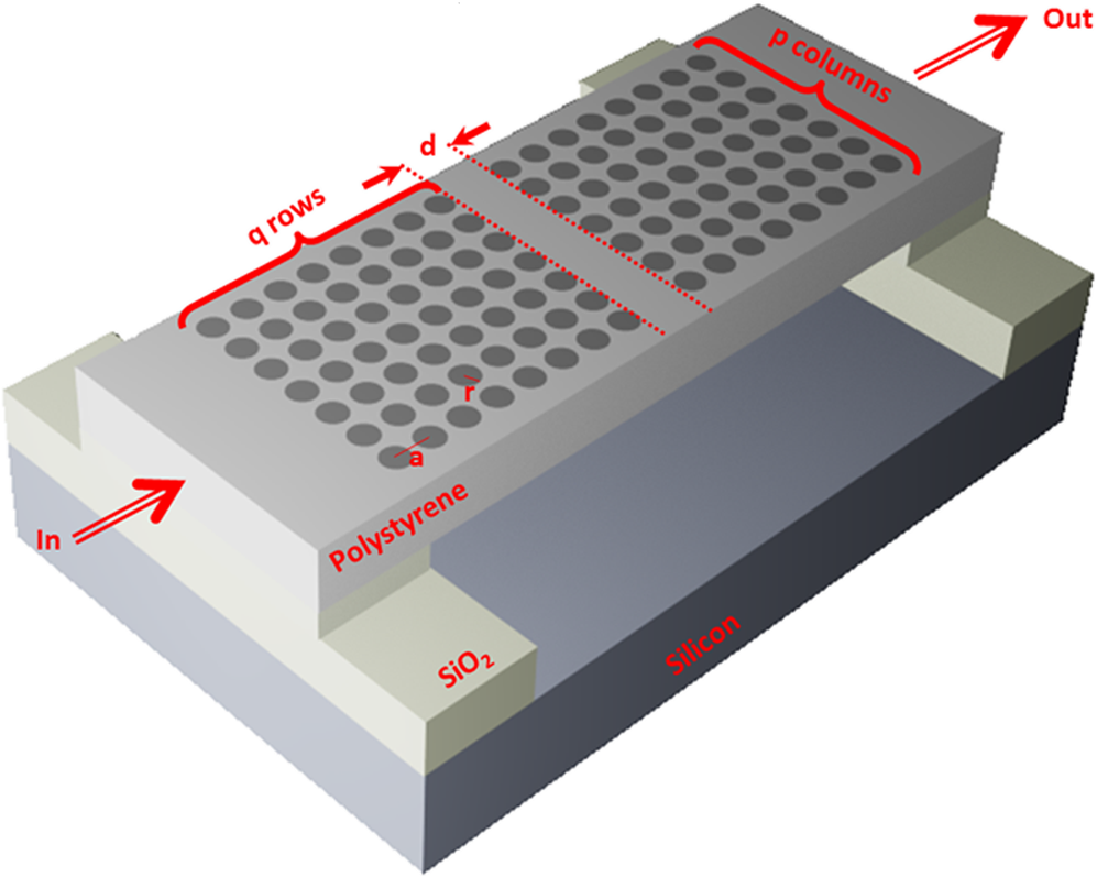 We denote the defect length, the lattice constant, and the hole radius with , , and , respectively. Nanoimprinting lithography, which allows a cost-effective and high throughput manufacturing of nanoscale devices, has been envisaged for the filter fabrication. In literature, the devices that are quite similar to the investigated one have been fabricated by e-beam lithography and reactive ion etching,15 focused ion beam etching,18 and nanoimprinting lithography.16,17 We believe that the latter fabrication technique is the most suitable, especially because of its low cost. Since our device is based on an air-suspended membrane and its performance is not significantly affected by the thickness of the polystyrene slab, which is not taken into account by the 2-D calculation methods, the device has been modeled by using the 2-D finite element method (FEM), which assures a good trade-off between results accuracy and computation time. We have also verified that the results obtained by 2-D FEM are close (difference ) to those of the 3-D FEM, especially for the resonance wavelength and transmission. A conservative evaluation of the quality factor has been demonstrated by the 2-D simulations when compared to the more accurate three-dimensional ones. Some thermoplastic polymers with different refractive index , i.e., polytetrafluoroethylene, , polyvinylidene fluoride, , polymethyl methacrylate (PMMA), , and polystyrene, , have already been evaluated by the authors for the membrane realization. Those polymers, especially PMMA and polystyrene, are the most used in nanoimprinting lithography because their viscosity can be easily changed to a large extent by only varying the temperature. The results reported in Refs. 21 and 22 allowed us to identify polystyrene as the most appropriate material because, among the four investigated polymeric materials, it is the only one allowing the formation of a complete bandgap for in-plane propagation directions. Moreover, polystyrene exhibits an excellent film quality.18 We assumed the polystyrene layer as deposited on an film laying on a silicon substrate. The air-suspended membrane can be realized by selectively removing the underneath the polystyrene. We have selected the square lattice of the planar PhC because it provides the highest value of attenuation within the bandgap in comparison with the hexagonal and the honey-comb lattices. Useful guidelines for the design and manufacturing of CWDM channel drop filters based on the investigated structures are provided in this paper. In particular, we have first designed a channel drop filter with central wavelength equal to 1551 nm, a pass-band width compliant with the target application, and low insertion loss. Then we evaluated the effect of random variations in the hole radius/shape, the lattice constant, and the defect length on the device performance. By using that approach, the fabrication tolerances have been estimated. Only a few preliminary results of the filter design, i.e., the dependence of the component performance on the defect length, were reported and briefly discussed in Ref. 23. 2.DesignThe target central wavelength of the designed filter is 1551 nm, which is one of the wavelengths defined by the G.694.2 CWDM wavelength grid. According to that standard, the pass-band width of each channel is . Therefore, the cavity -factor should be in the range from 97 to 155. The aims of our design are both the fulfilment of those requirements and the maximization of the resonance transmission, which strongly influences the device insertion loss. We initially assumed , , and . The dependence of the cavity resonance wavelength on the hole radius for several values of the defect length is shown in Fig. 2. As in all Fabry-Perot cavities where the resonance wavelength is proportional to the resonator length, the resonance wavelength of our PhC cavity increases as increases. As typical in all PhC cavities, in our device, the electromagnetic field at resonance is confined in both the defect region having and the holes of the rows close to the defect region. Since the resonance wavelength is proportional to the average refractive index of the medium where the field is confined at resonance, the radius of the air holes increases as the average index decreases, and thus the resonance wavelength decreases, too. Fig. 2Cavity resonance wavelength versus hole radius for several values of . , , . Dots are data points, while lines are fitting curves.  In the considered range of values, ranging from to , the fulfillment of the specification on the filter central wavelength implies a value ranging from to . It is well known that high -factor and high resonance transmission are conflicting requirements. Both and versus the hole radius are shown in Fig. 3. The -factor increases as the hole radius increases, while decreases when increases. The -factor monotonically increases as increases, while monotonically decreases as increases. Fig. 3(a) Quality factor dependence on the hole radius for several values of the defect length. (b) Resonance transmission versus hole radius for , , , and . , , . Dots are data points, while lines are fitting curves. 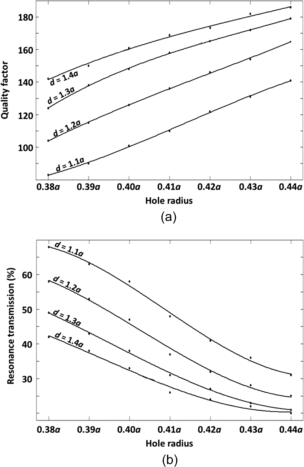 A good trade-off between the resonance transmission and the -factor can be achieved for and . For those geometrical parameters, the -factor is 115 (target to 155) and the resonance transmission is . For and , the filter central wavelength is equal to the target one, i.e., 1551 nm, and the device footprint is (). We have verified that the assumed values of and ( and ) are a good compromise between the performance enhancement and the footprint minimization. In fact, the increase of the column/row numbers implies an improvement of the -factor and a decrease of . Moreover, it obviously causes an increase of the device area. As and decreases, slightly increases and significantly decreases. For example, for and , the -factor is 240 and , while for and , we have and . As already mentioned, we have initially assumed for studying the influence of the hole radius and the defect length on the filter features. We have also demonstrated that this value of provides the best device performance, fulfilling the requirement of the ITU-T G.694.2 standard. In Figs. 4(a) and 4(b), both and versus the lattice constant have been reported for several values, suitably selecting the hole radius to obtain a resonance wavelength at 1551 nm. We have considered a range of from 580 to 640 nm to provide a -factor in the target range (). Higher values of have not been considered because the device fabrication is impossible for holes that are too large. Fig. 4(a) Quality factor and (b) resonance transmission dependence on the lattice constant for several values of the defect length with a suitable size of the hole radius to obtain the resonance condition at 1551 nm. The green areas represent the case studies compliant with the target range of the -factor. (c) Holes radius allowing the fulfilment of the requirement on the resonance wavelength for each couple of and values. Dots are data points, while lines are fitting curves. 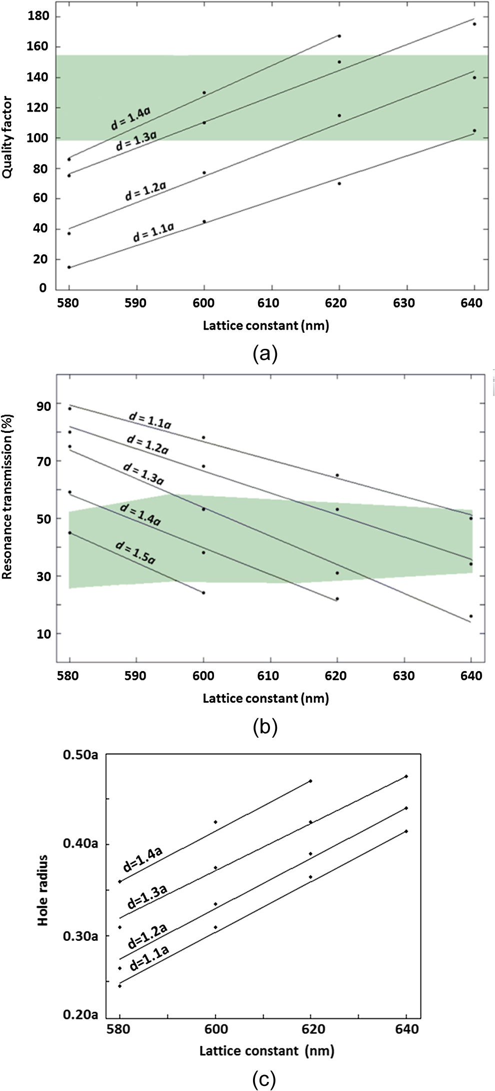 For each couple of and values, the radius allowing a resonance is shown in Fig. 4(c). The holes’ radius value allowing the fulfillment of the requirement on the resonance wavelength increases as the lattice constant and/or the defect length increase. Results in Figs. 4(a) and 4(b) confirm that high -factor and high resonance transmission are conflicting requirements. If we consider only the combinations of the geometrical parameters allowing the fulfillment of the constraint (green area), the condition , , and provides the highest value of , thus minimizing the insertion loss of the filter. 3.Fabrication TolerancesThe fabrication tolerances have been evaluated by investigating the effect of random variation in the filter geometry due to the potential fabrication imperfections on the cavity performance such as the resonance wavelength, the -factor, and the resonance transmission. In particular, we have randomly perturbed the hole radius, the lattice constant, the defect length, and the circular shape of the holes and have observed the impact of that perturbation on the performance parameters. The perturbations have been chosen so that their average value is zero, using a Gaussian random generator. We have simulated a lot of cavities to investigate the impact on the filter performance of random variation in the hole radius. The holes of each resonator have a radius , which is equal to where () is the nominal value of the radius and is the random perturbation term, which is obtained by a Gaussian random generator whose parameters are and . For each filter, we have calculated the resonance wavelength, the -factor, and the resonance transmission. As an example, the dependence of the average value of both and on the standard deviation is shown in Fig. 5. The average value of both the -factor and the resonance transmission decreases as the standard deviation increases, as expected. This means that a reduction of the uniformity of the holes radius implies a filter performance degradation. The -factor decrease is quadratic, while the decrease is linear.Fig. 5Dependence of the average -factor (a) and resonance transmission (b) on . Dots are data points, while lines are fitting curves. 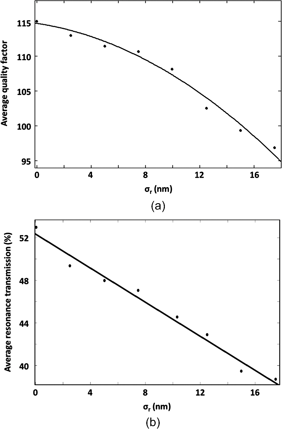 The histograms of the values of the -factor and the resonance wavelength for three values of , i.e., 2.5, 10.0, and 17.5 nm, are shown in Fig. 6. For , almost all the simulated filters () have a resonance wavelength in the range 1548 to 1554 nm and a -factor . When increases, the percentage of filters with a resonance wavelength in the range 1548 to 1554 nm and a -factor decreases. For , only 23% of the filters have a resonance wavelength in that range. On the basis of the specification assumed for the central wavelength and assuming a target production yield , we have derived that the fabrication tolerance allowed on the hole radius is equal to . This means that if the fabrication process is able to guarantee holes with a radius of , at least 70% of the produced device will be compliant with the requirements of the ITU-T G.694.2 standard. Fig. 6Histograms of the values of the resonance wavelength (a) and the quality factor (b) for three values of . 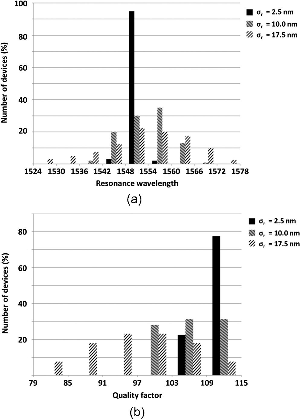 By using the same simulation technique described for the hole radius, we have evaluated the fabrication tolerance on the lattice constant. The uniformity of the lattice constant values is taken into account by the standard deviation . The simulation results have shown that the uniformity in the values of lattice constant decreases when increases. Figure 7 shows the histograms of the values of both the -factor and the resonance wavelength for three values of , i.e., 10, 20, and 30 nm. For , the predicted production yield is close to 80%. Assuming a target production yield , the fabrication tolerance on the lattice constant has to be . Fig. 7Histograms of the values of the resonance wavelength (a) and the quality factor (b) for three values of .  From both Figs. 6 and 7, we can conclude that the most critical performance parameter is the resonance wavelength. For example, for , all the simulated filters have a Q-factor , while only 30% of the devices has a resonance wavelength ranging from 1548 to 1554 nm. By investigating with the same approach the fabrication tolerance on the defect length, we have concluded that it is equal to . Finally, we have studied the effect of any perturbation of the circular shape of the holes. We have assumed that the fabrication imperfections may cause elliptical holes with a random eccentricity (when the eccentricity is zero, the ellipse degenerates in a circle). Our simulations allow us to conclude that the fabrication tolerance on the eccentricity is 0.06. Both the parameters of the designed filter and the fabrication tolerances are summarized in Table 1. The performance of designed filter, in terms of and , is comparable to the one exhibited by the fabricated cavities based on the same technology, which are reported in the literature.18,19 Table 1Geometrical and performance parameters of the designed filter. Fabrication tolerances are summarized.
4.ConclusionsGuidelines for the design and the fabrication of optical filters for CWDM applications based on a Fabry-Perot cavity in a polymer planar PhC are reported in this paper. They are derived by FEM simulations and are relevant to a number of crucial aspects such as the materials to be used, the holes’ radius/shape, the defect length, and the lattice configuration. Assuming that the device is fabricated through the nanoimprinting technique, a channel drop filter compliant with the ITU-T G.694.2 standard has been studied with particular attention to the fabrication tolerances. For the hole radius and the lattice constant, we have estimated a fabrication tolerance of , while the fabrication tolerance on the defect length, which is the most critical geometrical parameter, is close to 0.5%. Assuming that fabrication imperfections can lead to elliptical holes, the fabrication tolerance on the ellipse eccentricity has been evaluated as equal to 0.06. Since those tolerances are compliant with the resolution of the thermal nanoimprinting lithography,24 the achieved results point out the attractiveness of polymer PhC filters in the context of CWDM. CWDM drop filters that are available in the market are manufactured by either the silica planar lightwave circuit technology or the fiber technology. Those devices have a good reliability and a satisfactory thermal stability in the range 0 to 70°C. The insertion loss of those filters ranges from 1 to 3 dB and the adjacent channel isolation is of the order of 30 dB. The device that we have studied is surely more compact than the ones available in the market because its footprint is only , while the insertion loss/adjacent channel isolation of our filter are comparable to the ones exhibited by the components in the market. Experimental investigations, which will be our future work, are necessary to confirm that evaluation. ReferencesT. F. KraussR. M. De La Rue,
“Photonic crystals in the optical regime—past, present and future,”
Prog. Quantum Electron., 23
(2), 51
–96
(1999). http://dx.doi.org/10.1016/S0079-6727(99)00004-X PQUEAH 0079-6727 Google Scholar
R. M. De La RueC. Seassal,
“Photonic crystal devices: some basics and selected topics,”
Laser Photon. Rev., 6
(4), 564
–597
(2012). http://dx.doi.org/10.1002/lpor.201100044 1863-8880 Google Scholar
O. Painteret al.,
“Two-dimensional photonic band-gap defect mode laser,”
Science, 284
(5421), 1819
–1821
(1999). http://dx.doi.org/10.1126/science.284.5421.1819 SCIEAS 0036-8075 Google Scholar
S. Fanet al.,
“Channel drop filters in photonic crystals,”
Opt. Express, 3
(1), 4
–11
(1998). http://dx.doi.org/10.1364/OE.3.000004 OPEXFF 1094-4087 Google Scholar
M. QiuB. Jaskorzynska,
“Design of a channel drop filter in a two-dimensional triangular photonic crystal,”
Appl. Phys. Lett., 83
(6), 1074
(2003). http://dx.doi.org/10.1063/1.1599982 APPLAB 0003-6951 Google Scholar
H. Takanoet al.,
“Highly efficient multi-channel drop filter in a two-dimensional hetero photonic crystal,”
Opt. Express, 14
(8), 3491
–3496
(2006). http://dx.doi.org/10.1364/OE.14.003491 OPEXFF 1094-4087 Google Scholar
M. LeeP. M. Fauchet,
“Two-dimensional silicon photonic crystal based biosensing platform for protein detection,”
Opt. Express, 15
(8), 4530
–4535
(2007). http://dx.doi.org/10.1364/OE.15.004530 OPEXFF 1094-4087 Google Scholar
S. Zlatanovicaet al.,
“Photonic crystal microcavity sensor for ultracompact monitoring of reaction kinetics and protein concentration,”
Sens. Act. B: Chem., 141
(1), 13
–19
(2009). http://dx.doi.org/10.1016/j.snb.2009.06.007 SABCEB 0925-4005 Google Scholar
C. J. M. Smithet al.,
“In-plane microcavity resonators with two-dimensional photonic bandgap mirrors,”
IEE Proc. Optoelectron., 145
(6), 373
–378
(1998). http://dx.doi.org/10.1049/ip-opt:19982465 IPOPE8 1350-2433 Google Scholar
C. Ciminelliet al.,
“High Q guided-wave photonic crystal extended microcavity,”
in European Conf. on Optical Communication,
26
–27
(2004). Google Scholar
C. CiminelliF. PelusoM. N. Armenise,
“Modeling and design of two-dimensional guided-wave photonic band-gap devices,”
J. Lightwave Technol., 23
(2), 886
–901
(2005). http://dx.doi.org/10.1109/JLT.2004.838845 JLTEDG 0733-8724 Google Scholar
M. Loncaret al.,
“Design and fabrication of silicon photonic crystal optical waveguides,”
J. Lightwave Technol., 18
(10), 1402
–1411
(2000). http://dx.doi.org/10.1109/50.887192 JLTEDG 0733-8724 Google Scholar
W. Bogaertset al.,
“Fabrication of photonic crystals in silicon-on-insulator using 248-nm deep UV lithography,”
IEEE J. Sel. Top. Quant. Electron., 8
(4), 928
–934
(2002). http://dx.doi.org/10.1109/JSTQE.2002.800845 IJSQEN 1077-260X Google Scholar
F. Pommereauet al.,
“Fabrication of low loss two-dimensional InP photonic crystals by inductively coupled plasma etching,”
J. Appl. Phys., 95
(5), 2242
(2004). http://dx.doi.org/10.1063/1.1644630 JAPIAU 0021-8979 Google Scholar
C. Ligudaet al.,
“Polymer photonic crystal slab waveguides,”
Appl. Phys. Lett., 78
(17), 2434
(2001). http://dx.doi.org/10.1063/1.1366364 APPLAB 0003-6951 Google Scholar
C.-S. Keeet al.,
“Photonic band gaps and defect modes of polymer photonic crystal slabs,”
Appl. Phys. Lett., 86
(5), 051101
(2005). http://dx.doi.org/10.1063/1.1857069 APPLAB 0003-6951 Google Scholar
C.-G. Choiet al.,
“Air-suspended two-dimensional polymer photonic crystal slab waveguides fabricated by nanoimprint lithography,”
Appl. Phys. Lett., 90
(22), 221109
(2007). http://dx.doi.org/10.1063/1.2744482 APPLAB 0003-6951 Google Scholar
X. Huet al.,
“Fabrication of two-dimensional organic photonic crystal filter,”
Appl. Phys. B, 81
(6), 779
–781
(2005). http://dx.doi.org/10.1007/s00340-005-1943-x APBOEM 0946-2171 Google Scholar
M. Schmidtet al.,
“Ultralow refractive index substrates—a base for photonic crystal slab waveguides,”
Appl. Phys. Lett., 85
(1), 16
(2004). http://dx.doi.org/10.1063/1.1767962 APPLAB 0003-6951 Google Scholar
Coarse Wavelength Division Multiplexing (Technologies and Applications), Taylor & Francis, Boca Raton, FL
(2007). Google Scholar
C. CiminelliM. N. Armenise,
“Material optimization in the design of a 2D guided-wave polymer photonic crystal filtering device,”
in Proc. of the Integrated Photonics and Nanophotonics Research and Applications Conference,
(2007). Google Scholar
C. CiminelliM. N. Armenise,
“Modelling and design of a 2D photonic crystal microcavity on polymer material for sensing applications,”
Proc. SPIE, 6619 661933
(2007). http://dx.doi.org/10.1117/12.738607 PSISDG 0277-786X Google Scholar
C. Ciminelliet al.,
“Design of a polymer photonic crystal membrane cavity for channel drop filtering in coarse wavelength division multiplexing networks,”
in Proc. of the 15th International Conference on Transparent Optical Networks,
23
–27
(2013)). Google Scholar
C. PerozV. ReboudC. M. S. Torres,
“Nanoimprint technologies,”
Nanofabrication: Techniques and Principles, 117
–140 Springer-Verlag, Wien, Austria
(2012). Google Scholar
Biography Francesco Dell’Olio received, in 2005 and 2010, his master’s degree (cum laude) in electronic engineering and his PhD in information engineering both from the Politecnico di Bari, Italy. His research interests include the fields of integrated optical sensors, especially angular velocity and chemical sensors, silicon photonics, and InP-based photonic integrated circuits. He is the coauthor of a book published by Springer, 20 papers published in international refereed journals, and more than 40 papers published in conference proceedings. His papers have been cited about 400 times and his h-index is 9. He is a member of OSA, and he serves as reviewer for several high impact factor journals such as Optics Express, Optics Letters, and IEEE Photonics Journal. Finally, he has been involved in several research projects on miniaturized optical gyroscopes, optical links for data handling on-board of satellites, sensor systems for harsh environments monitoring, and electromagnetic field photonic sensors.  Caterina Ciminelli received her Laurea degree in electronic engineering in 1996 and PhD in electronic engineering in 2000, both at Politecnico di Bari, Italy. From 1999 to 2002, she did industrial research activity on optoelectronic components and subsystems at the R&D Division of Pirelli Optical Systems, Milan, and CiscoPhotonics Italy, Monza. In May 2002, she joined Politecnico di Bari as assistant professor of electronics. Since April 2012 she has been an associate professor at Politecnico di Bari. Her scientific interests are in the field of optics and guided-wave optoelectronics, in particular, on fabrication, characterization, modeling, and design of devices for optical switching, filtering and sensing, photonic bandgap devices, lasers, and semiconductor optical amplifiers. She is author or coauthor of more than 150 papers. She is a member of OSA and IEEE and serves as referee of several international journals. She is involved in several research programs, also as coordinator.  Donato Conteduca graduated in electronic engineering at the Politecnico di Bari, Italy, in 2011. He is currently a graduate student for the MSc degree in electronic engineering at the Politecnico di Bari. His research interests are in the field of silicon photonics, photonic crystals, plasmonic devices, and biosensors. He spent most of his internship of the MSc degree at Microphotonics and Photonic Crystals Group at University of St. Andrews, Scotland.  Mario Nicola Armenise received his Laurea degree in electrical engineering from the University of Bari, Italy. He has been a full professor of optoelectronics since 1986 at Politecnico di Bari. He has been deputy rector of the Politecnico di Bari from 1994 to 1997. He has been deputy chair of the Consortium of the Apulian Universities (CIRP) from 1995 to 1997 and chair from 2004 to 2011. He was president of the Italian Optics and Photonics Society and is a fellow of the European Optical Society. Since June 2011, he has been president of the Italian Electronics Association. He is author or coauthor of more than 330 journal articles and conference presentations, and coinventor of three international patents. His research interests include fabrication and characterization techniques of optical waveguides and devices, design and simulation of guided wave devices and circuits for telecommunications, optical signal processing, optical computing, and sensing. |


