|
|
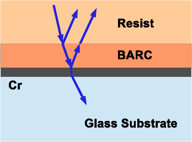
1.IntroductionOptical systems somtimes require components that are made with photolithography on glass substrates. Photomasks for projection or contact lithography are perhaps the most prominent examples. Photomasks are a specialized form of optical elements known as diffractive optics or computer-generated holograms (CGHs), which are fabricated using lithographic patterning technologies. CGHs are now used in many applications to shape and modify optical wavefronts.1,2 In many cases, the fabrication process for CGHs takes a cue from the entrenched fabrication process for semiconductor lithography photomasks. The hologram is fabricated by patterning a chromium layer on a glass substrate.3–8 The result is a binary amplitude hologram with transparent and opaque fringes. A binary amplitude hologram can be converted into a binary phase hologram by etching the area of the glass substrate that is not covered by the chromium mask using a reactive ion etching (RIE) process followed by removal of the chromium layer. In this paper, we revisit this fabrication process for CGHs and describe an alternative process that is simpler than the established chromium-on-glass process, performs better with high numerical aperture (NA) photolithography tools, and offers greater process flexibility. 2.Bottom Antireflection LayersCGHs are frequently fabricated using maskless laser lithography tools, which use optics with increasing NA to enable the writing of patterns with smaller and smaller feature sizes. For example, the zone plate array lithography (ZPAL) tool9,10 in the Nano-Structured Optics Laboratory at the National Institute of Standards and Technology (NIST) uses arrays of beamlets with NAs of 0.6 or 0.8 to achieve feature sizes down to for the lenses and for the focusing lenses. The exposure wavelength is 405 nm, the wavelength emitted by high-power gallium-nitride solid-state lasers, which are now used in many maskless laser lithography tools. With decreasing feature size, tight control of the lithography process is required. It is especially important to suppress the reflection of light into the photoresist film at the resist–substrate interface. Optical interference of light in the resist film otherwise results in uneven resist exposure and poor feature dimension control.11 Figure 1 shows a cross-section through a chromium-on-glass photomask. When a chromium layer is patterned with lithography, suppression of the reflection by the chromium layer is clearly important because of the high refractive index of chromium and the resulting high reflectivity at a chromium–resist interface. Chromium layers are typically thick. We discuss different types of bottom antireflection coating (BARC) between the resist and chromium layers in this paper. Conventional photomasks are often made with a chromium oxide (CrO) antireflection layer to attenuate the reflection of light from the chromium layer into the resist.12 Advanced photomasks use organic ARCs that achieve lower reflectivity.12 Organic coatings are also useful when substrates are prepared on a small scale in a laboratory setting because they can be applied using a simple spin-coating process. The effect of a BARC between the chromium and the photoresist on the reflection of light into the photoresist layer is shown in Fig. 2. The figure shows the reflectivity into the resist at 405 nm for a CrO ARC and also for two commercially available organic BARCs, BARLi and WiDE, as a function of BARC thickness. The reflectivity was calculated using Snell’s law and the Fresnel equations at each material interface with the well-known transfer matrix method (see, e.g., Ref. 13). The reflectivities for s- and p-polarized light were averaged. Refractive indices and extinction coefficients for the polymer materials were measured at NIST using ellipsometry (with the exception of the data for the WiDE coating, which were provided by the supplier). Data for the refractive index of the borosilicate float glass that we used as a substrate material were available from the manufacturer (Schott BOROFLOAT 33, Schott, Germany). The refractive index of chromium at our wavelength of interest has been published.14 Fig. 2Reflectivity into the photoresist in a chrome-on-glass photomask for different types of antireflection layer. 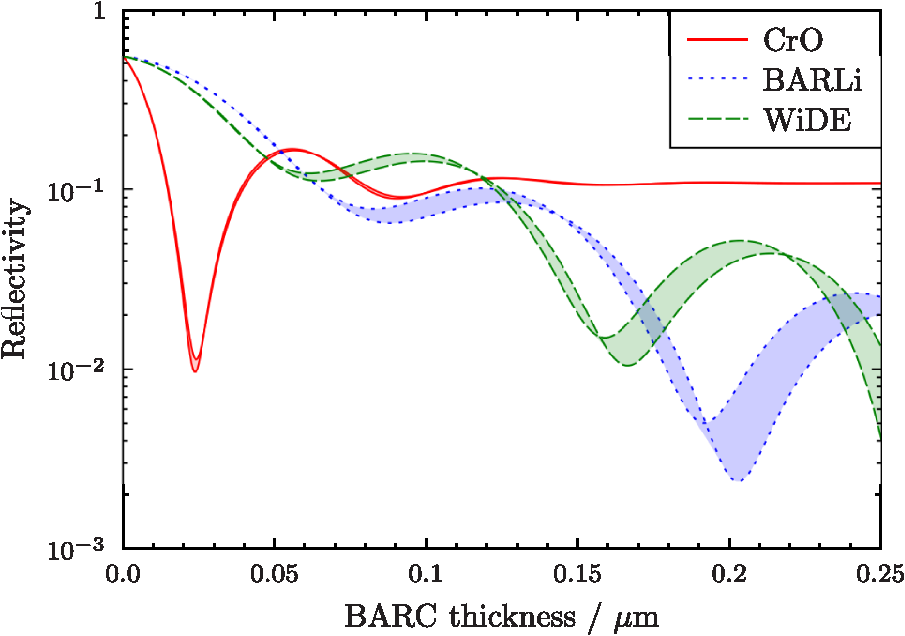 The reflectivity of the photoresist–BARC interface was calculated for a set of angles of incidence with a 0.5 deg spacing between normal incidence and the maximum angle of incidence. The reflections at the glass substrate back surface and at the resist top surface were ignored in the calculations. Figure 2 shows the reflectivities for normal incidence (dotted lines) and for the maximum angle of incidence in a focused beam with in air (solid lines). The maximum angle of incidence inside a resist layer with a refractive index of 1.71 for an beam is close to 20 deg. The shaded areas indicate the range of reflectivities that are obtained at all angles between normal incidence and the maximum angle at a given BARC thickness. The CrO coating reduces the reflectivity into the resist from for a chromium–resist interface without antireflection layer to . Figure 2 also shows the reflectivity that can be achieved on chromium layers with two commercially available organic BARC materials (BARLi and WiDE). BARC materials that are easily available commercially are optimized for an exposure wavelength of 365 nm (i-line) and are typically intended to be used on silicon, which has a much larger refractive index in the ultraviolet than chromium. It is therefore not surprising that the performance of these materials as antireflection layers on chromium is somewhat disappointing. With the BARLi BARC, it is at best possible to reduce the reflectivity at the bottom of the resist layer to . Exposure tests that we made with the ZPAL lithography tool at NIST showed that it was difficult to obtain good exposures on chromium layers with the commercial BARC materials. We found that lithographic patterning of glass substrates is best done by patterning the glass without the use of a chromium layer. The reflectivity of a glass–resist interface is , as can be seen in Fig. 3. The reflectivity is much lower than that of the resist–chromium interface, but we found that it is not sufficiently low to avoid noticeable interference effects. In our search for a suitable material for an antireflection layer, we discovered that an index matching layer of a readily available lift-off resist based on a poly-dimethyl glutarimide (PMGI) polymer results in excellent suppression of reflected light. The reason is a fortuitous coincidence: the refractive index of the PMGI layer at 405 nm (1.61) is close to the geometric mean of the refractive indices of the glass substrate (1.59) and the photoresist (1.71), which results in near-perfect suppression of the reflection by a quarter-wave antireflection layer.13 The reflectivity into the photoresist of a PMGI layer on a borosilicate glass substrate is shown in Fig. 3, together with the reflectivity of the two commercial ARCs that are also shown in Fig. 2. The reflectivity for the PMGI layer has two minima close to at PMGI thicknesses of 60 nm (1/4 wave) and 190 nm (3/4 wave), at which it performs far better than the other ARCs. Fig. 3Reflectivity into the photoresist for a glass substrate and a photoresist with with different types of antireflection layer. 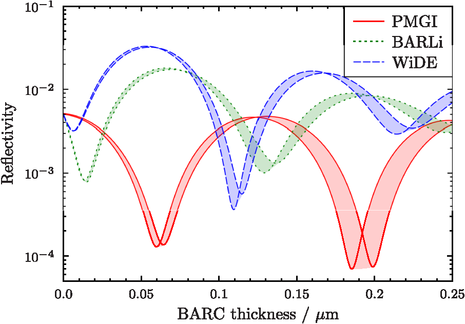 Figure 4 shows a portion of a test grating with 500-nm wide lines written on a substrate made from borosilicate float glass that was coated with a bilayer resist consisting of 190-nm PMGI and positive photoresist. The test grating was written with the ZPAL lithography tool at NIST using beamlets with an NA of 0.6. The dark areas in Fig. 4 were exposed and the resist was removed during development. Fig. 4Optical micrograph of 500-nm wide lines, written with a zone plate array lithography photolithography tool,9 in 400-nm positive i-line photoresist with a 190-nm-thick layer of a poly-dimethyl glutarimide based lift-off resist as an antireflection layer on a borosilicate float glass substrate. 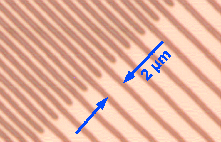 3.Summary and ConclusionsWe have demonstrated that a PMGI layer can be an excellent antireflection layer between a glass substrate and a photoresist for photolithography at 405 nm with high-NA laser lithography tools. PMGI polymers are widely used as resist materials for deep-ultraviolet lithography, electron-beam lithography, and also as a material for lithographic “lift-off” processes.15 They are readily available as spin-on materials in a range of formulations. Using a PMGI layer as index matching layer between a glass substrate and photoresist has several advantages over conventional chromium-on-glass material stacks for the fabrication of diffractive optics and CGHs. A PMGI bottom ARC also provides good process latitude. Figure 3 shows that the reflectivity for a beam with remains below for a large range of coating thicknesses between 180 and 205 nm; precise thickness control and coating uniformity are therefore not critical. The PMGI polymer is soluble in water-based alkaline developers and is removed during the development process together with the photoresist. With a PMGI thickness of 190 nm and a photoresist thickness between 300 and 400 nm, the total thickness of the resist layer is between 500 and 600 nm. Phase profiles with a range exceeding can be etched into the glass substrates using an RIE process for all visible wavelengths because the etch rate of glass is approximately three times that of the polymer resist. The erosion of resist walls during the etching process can, potentially, result in a widening of lines that are etched into the glass substrate. This effect can be minimized by careful optimization of the etching process.16,17 For the fabrication of amplitude holograms, the same bilayer resist can be used, except that the order of metal coating and lithography are now reversed. The metal layer is deposited on the glass substrate after exposure and developing, and the resist is then removed (lifted off). In this way, wet etching of the metal layer is avoided, which is a process step that can be difficult to control in a laboratory setting. A more important advantage is that any metal can be deposited without the need to adapt the properties of the resist layers to the optical properties of the metal film. A toolbox of functions for the calculation of optical multilayer properties, written in the GNU Octave language,18 was developed to calculate the resist stack reflectivities. The toolbox and refractive index data are available from the authors upon request. AcknowledgmentsOur research was in part performed at the National Institute of Standards and Technology (NIST) Center for Nanoscale Science and Technology. We are grateful to the staff of the NanoFab at the NIST Center of Nanoscale Science and Technology, in particular, Dr. Lei Chen, for many helpful discussions, for providing photoresist materials, and for equipment that was used in our work. Disclaimer: The full description of the procedures used in this paper requires the identification of certain commercial products and their suppliers. The inclusion of such information should in no way be construed as indicating that such products or suppliers are endorsed by NIST, or are recommended by NIST, or that they are necessarily the best materials or suppliers for the purposes described. ReferencesW. B. Veldkamp,
“Binary optics and beyond: where do we go from here?,”
Jpn. J. Appl. Phys., 45
(8B), 6550
–6554
(2006). http://dx.doi.org/10.1143/JJAP.45.6550 JJAPA5 0021-4922 Google Scholar
B. KressP. Meyrueis, Digital Diffractive Optics, John Wiley & Sons, Chichester
(2000). Google Scholar
H. G. Rheeet al.,
“Performance evaluation of laser lithographic machine for computer generated hologram,”
Int. J. Adv. Manuf. Technol., 52
(9–12), 1005
–1009
(2011). http://dx.doi.org/10.1007/s00170-010-2803-3 IJATEA 1433-3051 Google Scholar
F.-Z. Liet al.,
“Test of off-axis aspheric surfaces with CGH (in Chinese),”
Opt. Precis. Eng., 19
(4), 709
–716
(2011). Google Scholar
A. G. Poleshchuket al,
“Computer generated holograms: fabrication and application for precision optical testing,”
Proc. SPIE, 7102 710206
(2008). http://dx.doi.org/10.1117/12.797816 PSISDG 0277-786X Google Scholar
R. Schreineret al.,
“Computer generated holograms for the optical shop testing of aspheres,”
Proc. SPIE, 5856 503
–508
(2005). http://dx.doi.org/10.1117/12.612577 PSISDG 0277-786X Google Scholar
A. G. Poleshchuket al.,
“Polar coordinate laser pattern generator for fabrication of diffractive optical elements with arbitrary structure,”
Appl. Opt., 38
(8), 1295
–1301
(1999). http://dx.doi.org/10.1364/AO.38.001295 APOPAI 0003-6935 Google Scholar
S. M. ArnoldR. Kestner,
“Verification and certification of CGH aspheric nulls,”
Proc. SPIE, 2536 117
–126
(1995). http://dx.doi.org/10.1117/12.218414 PSISDG 0277-786X Google Scholar
H. I. Smithet al.,
“An innovative tool for fabricating computer-generated holograms,”
J. Phys.: Conf. Ser., 415 012037
(2013). Google Scholar
R. Menonet al.,
“Zone-plate-array lithography (ZPAL): optical maskless lithography for cost-effective patterning,”
Proc. SPIE, 5751 330
–339
(2005). http://dx.doi.org/10.1117/12.598742 PSISDG 0277-786X Google Scholar
C. A. Mack, Fundamental Principles of Optical Lithography: The Science of Microfabrication, John Wiley & Sons, London
(2007). Google Scholar
B. M. Rathsacket al.,
“Lithography simulation of sub-0.30 micron resist features for photomask fabrication using i-line optical pattern generators,”
Proc. SPIE, 3873 484
–492
(1999). http://dx.doi.org/10.1117/12.373343 PSISDG 0277-786X Google Scholar
O. S. Heavens, Optical Properties of Thin Solid Films, Dover Publications, New York
(1991). Google Scholar
L. W. BosD. W. Lynch,
“Optical properties of antiferromagnetic chromium and dilute Cr-Mn and Cr-Re alloys,”
Phys. Rev. B, 2
(11), 4567
–4577
(1970). http://dx.doi.org/10.1103/PhysRevB.2.4567 PRBMDO 1098-0121 Google Scholar
L. ChenQ. WangU. Griesmann,
“Plasma etching uniformity control for making large and thick dual-focus zone plates,”
Microelectron. Eng., 88
(8), 2466
–2469
(2011). http://dx.doi.org/10.1016/j.mee.2011.01.009 MIENEF 0167-9317 Google Scholar
Q. WangL. ChenU. Griesmann,
“A simple method to improve etching uniformity when making phase type CGHs on a thick glass substrate,”
in Optical Fabrication & Testing 2010OSA Technical Digest Series,
(2010). Google Scholar
J. W. EatonD. BatemanS. Hauberg, GNU Octave Manual Version 3, Network Theory Limited(2008). Google Scholar
Biography Quandou Wang is an optical engineer with the National Institute of Standards and Technology (NIST). He received his PhD from the Changchun Institute of Optics, Fine Mechanics and Physics (CIOMP), Chinese Academy of Sciences, China, in 2001. He was with CIOMP from 1992 to 2001. He then joined the Optical Sciences Center, University of Arizona, from 2001 to 2002, working on computer-controlled optical fabrication and testing of aspherical surfaces. Since 2002, he has worked on metrology of precision surfaces at the NIST. His current research interests include optical testing and precision interferometric metrology, optomechanics, and design and fabrication of diffractive and nanostructured optics and their application to surface metrology.  Ulf Griesmann is a physicist with the NIST. He received his Dr.rer.nat degree from the University in Bonn, Germany, in 1992. He worked as a postdoc on atomic spectroscopy with short-wavelength lasers at Imperial College London, United Kingdom. After coming to NIST in 1994, he worked on precision spectrometry and properties of optical materials. His current research interests include optical phase measuring interferometry, precision surface metrology, methods for absolute metrology, metrology of free-form surfaces, and the application of nanostructured optics to the metrology of aspheric and free-form surfaces. |