|
|
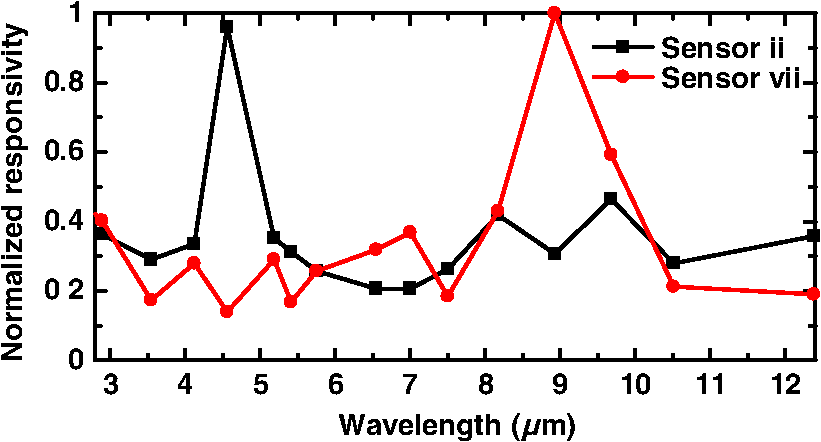
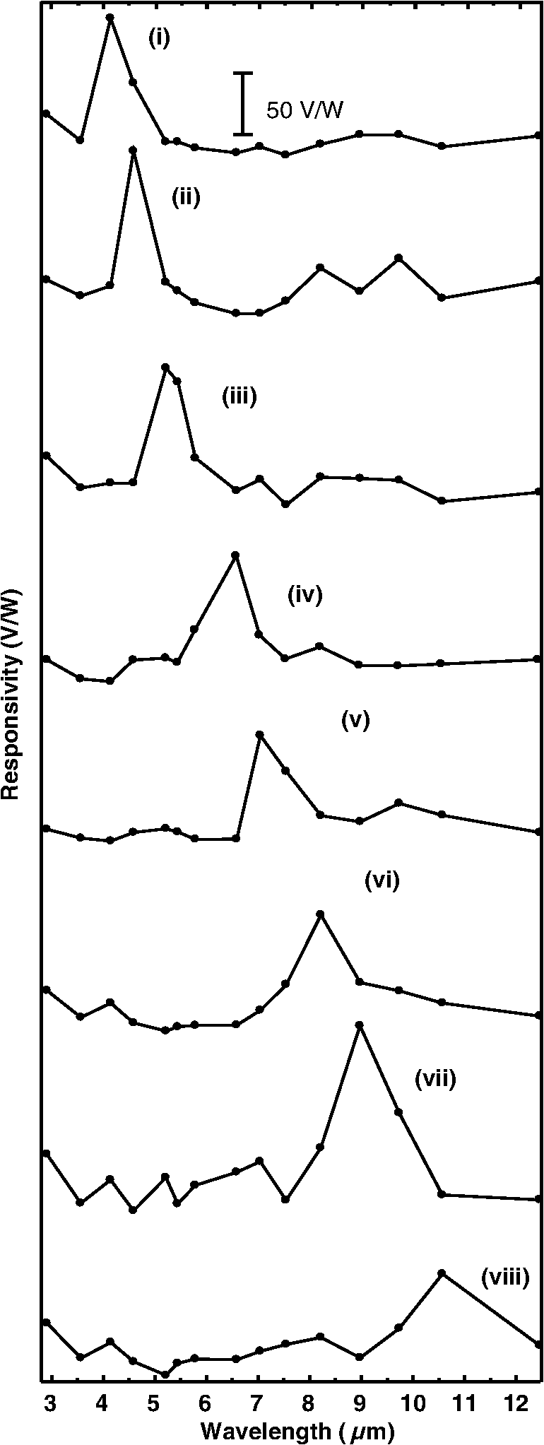
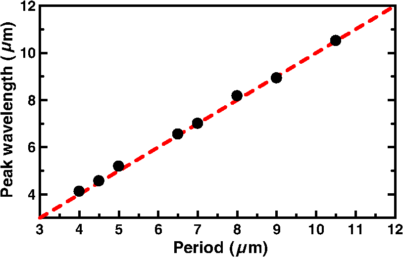
1.IntroductionThere has been increasing interest in the advanced functions of uncooled infrared (IR) image sensors with microelectromechanical system (MEMS)-based pixel structures1 to expand the applications of IR sensing.2 In particular, there is much in a spectral discrimination function that enables uncooled IR sensors to identify objects through their radiation spectrum, which is useful for many applications such as fire detection and gas analysis. A pixel array in which each pixel has a different absorption wavelength could be used to realize multicolor imaging at IR wavelengths, which would provide the same benefits as the RGB pixels of image sensors in the visible region. Therefore, wavelength selectivity is a promising function for an advanced IR sensing.3 Many approaches have been proposed to achieve this, such as band-pass filters,4 optical resonant structures,5,6 and multilayer structures.7–11 However, the attachment of external optical systems requires additional space and increases the cost. The optical resonant structures and multilayer structures require gap or thickness control of the dielectric layer to achieve maximum absorption according to the wavelength.5,10 Therefore, such typical approaches have difficulty in integrating different pixels in an array for a multicolor imaging. We have applied plasmonics to address this challenge. A great deal of interest has developed in plasmonics,12–14 in which a metal surface structure provides the means for the novel manipulation of photons. Significant advances in the field of photonic crystals15–17 and micro/nanofabrication techniques have lead to considerable progress in plasmonics during the last decade. A periodical metal surface structure, referred to as a plasmonic crystal,18 was reported to have significant potential for the expansion of the operating wavelength region beyond the near-IR region.19–22 Thus, plasmonics is a promising technology for the control of light over a wide spectral range. Recently, we have reported a wavelength selective uncooled IR sensor that employs plasmonics and functions in the middle-wavelength IR region (MWIR)23 and partially in the long-wavelength IR region (LWIR).24 However, the wavelength selectivity for both MWIR and LWIR has not yet been reported in detail. In this study, we report the wavelength selectivity of a sensor for both MWIR and LWIR. 2.DesignFigure 1(a) shows a schematic of the Au-based two-dimensional plasmonic absorber (2-D PLA) used as a thermopile, which is a type of uncooled IR sensor. The 2-D PLA has a 2-D periodic array of round dimples on the surface, where photons can be manipulated by spoof surface plasmon polaritons (SPPs).22 Such an asymmetric structure as a one-dimensional grating produces a strong polarization dependency, which is disadvantageous for the IR image sensors. Therefore, a 2-D surface structure with a square lattice and a round dimple was adopted, where only the thin surface metal layer absorbs the incident light. Fig. 1(a) Schematic diagram of the uncooled IR sensor (thermopile) with Au-based two-dimensional plasmonic absorber (2-D PLA). (b) Calculated wavelength absorption results for the 2-D PLA as a function of the period. (c) Concept of the pixel array with various 2-D PLAs for multispectral imaging. 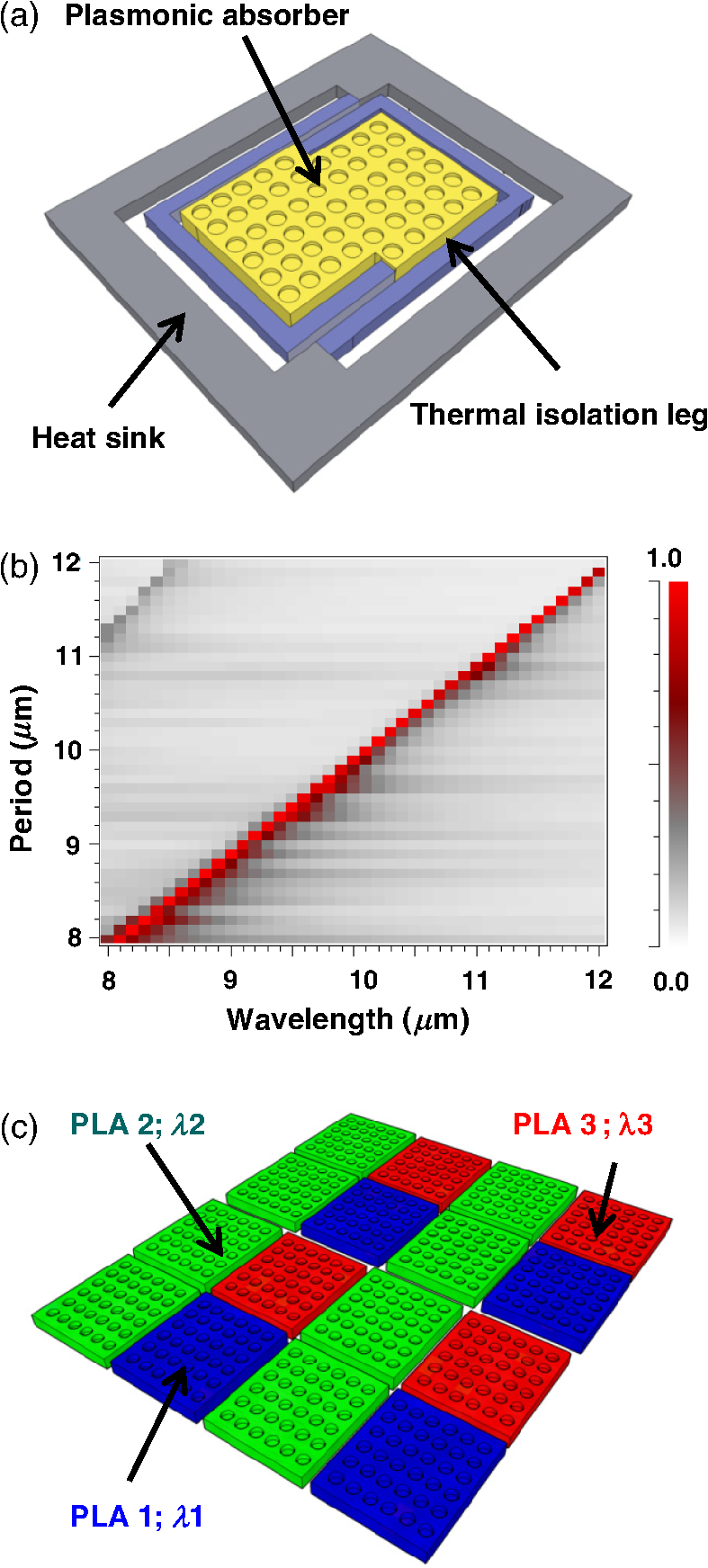 We have previously reported the absorption properties of a PLA in the MWIR region,23 where the absorption wavelength was almost the same as the period of the 2-D PLA, due to the spoof SPP mode. The basic design of the Au-based 2-D PLA as an IR absorber for the LWIR at normal incidence was achieved using the rigorous coupled wavelength analysis method. Figure 1(b) shows the wavelength absorption of the Au-based 2-D PLA as a function of the period from 8.0 to 12.0 μm with a fixed dimple diameter of 6.0 μm and a depth of 1.5 μm. The strong wavelength selective absorption is evident over the LWIR region, as for the MWIR region,23 and this can be controlled according to the surface period. This satisfies the requirements for an uncooled wideband IR sensor with the wavelength selective function. Figure 1(c) shows the concept of 2-D PLAs with various surface pixel array structures, where three different 2-D PLAs with different absorption wavelengths (, , and ), were employed. Multicolor imaging can be realized by controlling only the surface structural parameters, such as the dimple period and diameter. 3.Sensor FabricationA MEMS-based uncooled IR sensor with 2-D PLAs was developed. The 2-D PLAs are fabricated by forming a Au layer on perforated . However, the back side of the layer absorbs scattered light in the LWIR region. To address this issue, an Al layer is introduced to the back side of the 2-D PLA to reflect scattered light. Figure 2 shows the process used to fabricate the MEMS-based thermopile with the 2-D PLA: (a) The devices are fabricated on 6-in p-type Si(1 0 0) substrates using a standard complementary metal oxide semiconductor (CMOS) process. The thermocouples consist of a series of p- and n-types polysilicon, of which the resistivities are controlled by ion implantation. The Al layer is formed as a back side reflection layer under the absorber area. The etching holes for the bulk-micromachining are formed by reactive-ion etching (RIE). A 1.5-μm thick layer is formed on the absorber area. (b) The periodic structure is formed only on the of the IR absorber area by RIE. (c) thick Cr/Au layers are sputtered, where the Cr layer acts as an adhesion layer between and Au. The 250-nm thick Au layer is sufficiently thicker than the penetration depth in the IR wavelength region, so that absorption by beneath the Au layer is negligible. The Cr/Au layers are selectively etched using a wet etchant to reveal the etching holes covered by sputtering. Scanning electron microscopy (SEM) observation confirmed that the Cr/Au layers were uniformly coated on both the bottom and side walls of the etched holes to complete the concave Au structure. (d) The wafers are diced into chips. The Si is anisotropically etched using tetramethylammonium hydroxide through the etching holes to form the cavity under the IR absorber area. Finally, a thermally isolated freestanding structure is completed on which the 2-D PLA is formed. Fig. 2Schematic diagram of the procedure used to fabricate the MEMS-based thermopile with 2-D PLA. (a) Devices are formed on the surface of a Si wafer using a standard complementary metal oxide semiconductor process. Etching holes are formed by reactive-ion etching. (b) The periodic hole structures are formed on using a dry etching process. (c) Cr/Au layers are sputtered on the perforated . (d) The thermally isolated freestanding structure is completed by bulk-micromachining. 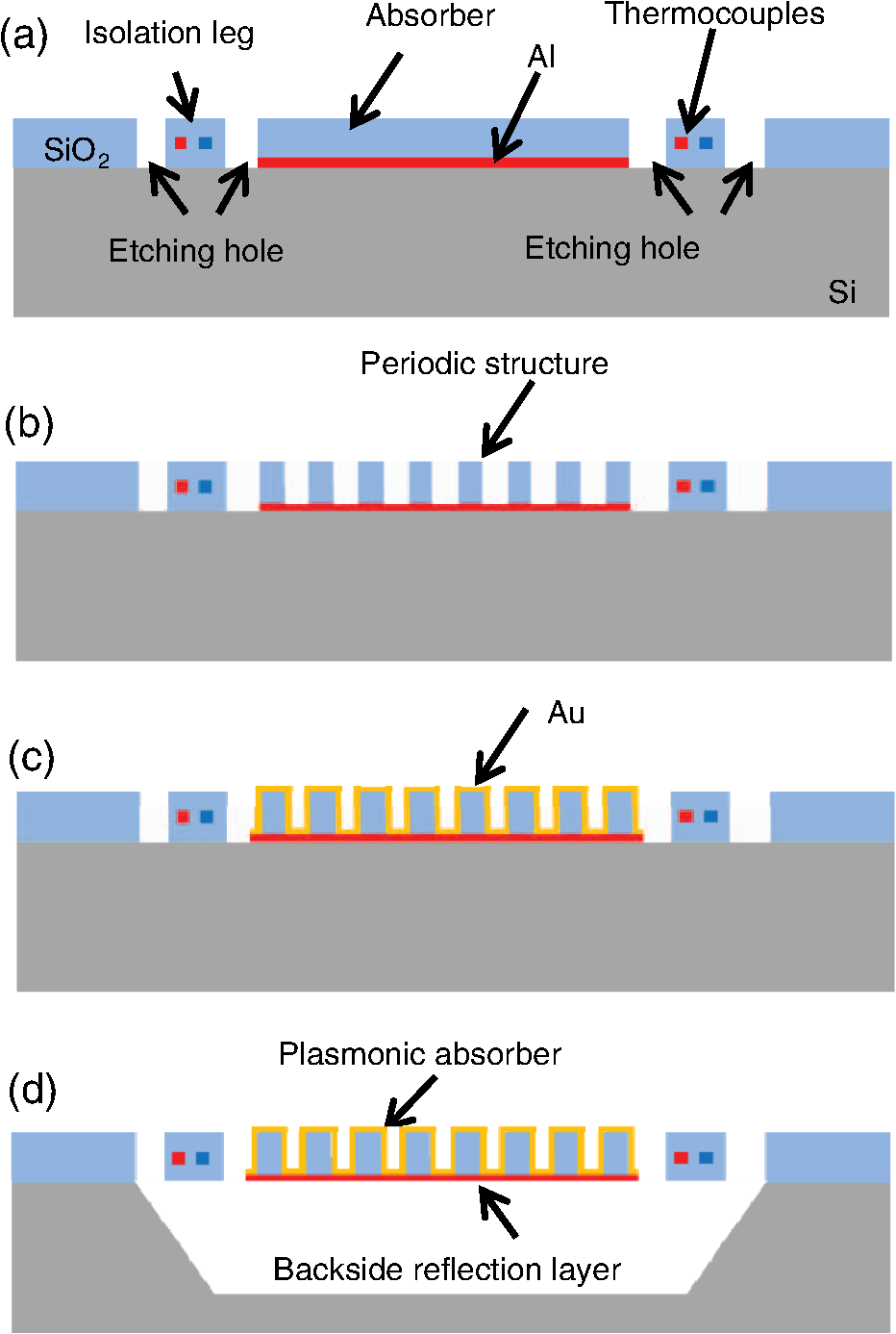 Figure 3(a) shows an SEM image of the developed thermopile. The detector area, which is , is surrounded by the long thermal isolation legs to reduce the thermal conductance. Various sensors with different 2-D PLA structures were fabricated on the same wafer. The respective diameters and periods of the surface structures were as follows: (i) 3.0 and 4.0 μm, (ii) 3.0 and 4.5 μm, (iii) 4.0 and 5.0 μm, (iv) 4.0 and 6.5 μm, (v) 6.0 and 7.0 μm, (vi) 6.0 and 8.0 μm, (vii) 6.0 and 9.0 μm, and (viii) 6.0 and 10.5 μm. The depth was fixed at 1.5 μm for all sensors. Fig. 3(a) Scanning electron microscopy (SEM) image of the microelectromechanical system-based thermopile with 2-D PLA developed in this study. Magnified SEM images of the 2-D PLAs of sensors (b) (ii) and (c) (vii). (d) Schematic diagram of the 2-D PLA. 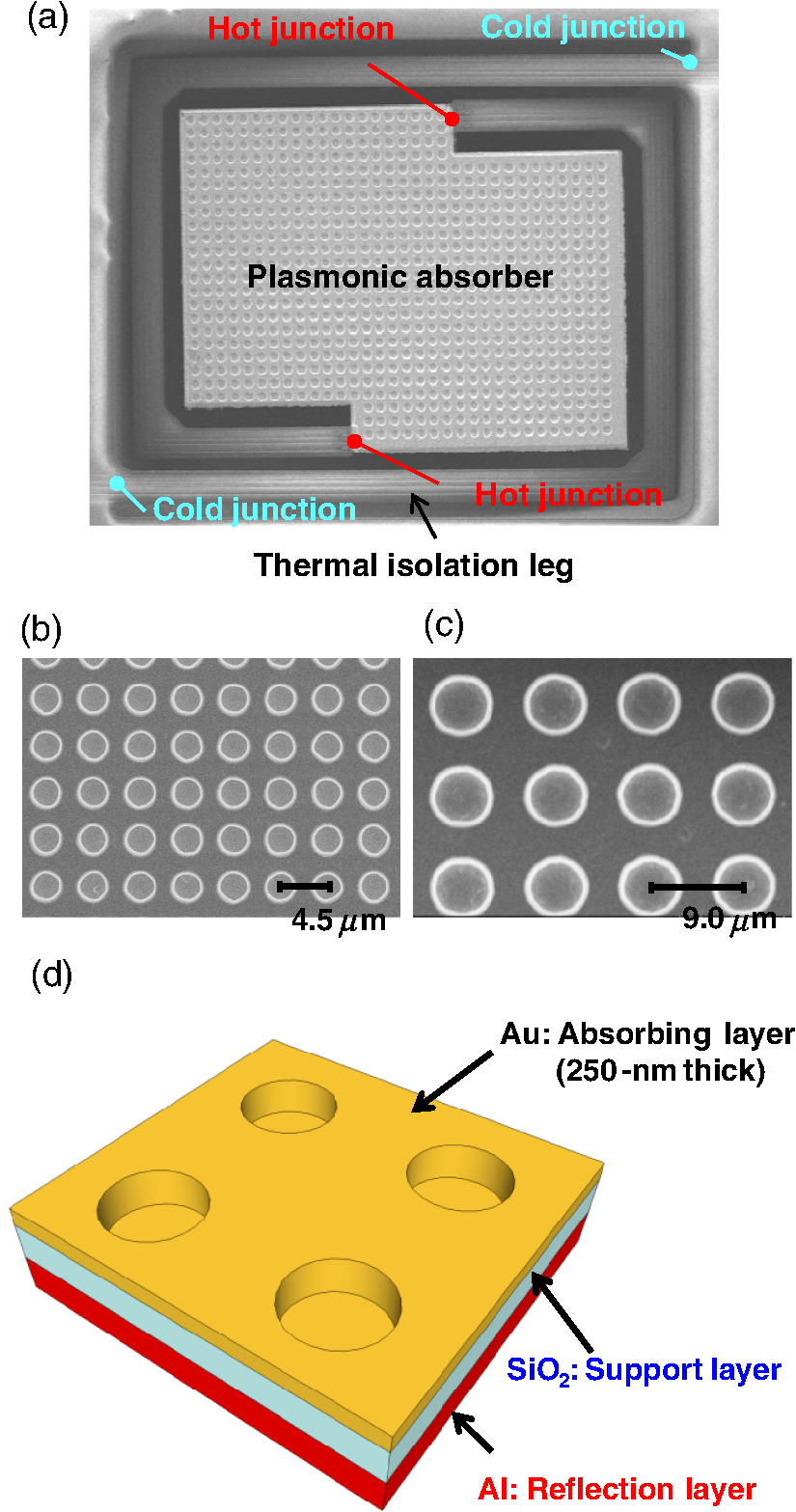 Figures 3(b) and 3(c) show representative magnified SEM images of two 2-D PLA surfaces. Two periodic structures of 2-D PLA were formed, denoted sensors (ii) and (vii) for MWIR and LWIR, respectively. The diameters and periods of the surface structures of sensor (vii) are linearly twice those of sensor (ii). The depth was fixed at 1.5 μm for both sensors. Figure 3(d) shows a schematic of the 2-D PLA structure with the Al reflection layer. 4.MeasurementsThe wavelength selective properties of the 2-D PLA were investigated. The sensors were set in a vacuum chamber with a Ge window under a pressure of 1 Pa to prevent thermal conduction loss through the atmosphere. The sample was irradiated with IR rays from a blackbody through narrow band-pass filters for the selection of the evaluation wavelengths. The typical full width at half maximum was 80 nm. A pinhole was used to restrict the incident light to the 2-D PLA region only. The output voltage was measured and the responsivity was calculated as the ratio between the output voltage difference of the on and off states and the input power. The input power was calculated according to the measurement system parameters, absorber area, transmittance from the blackbody to the sensor through the atmosphere, narrow band-pass filters and the Ge window, and the spectral radiant emittance equation at the evaluated wavelength as previously reported.23 The responsivities of sensors (ii) and (vii) were measured first. Figure 4 shows the normalized responsivity of both sensors with clear responsivity peaks in the MWIR and LWIR regions, which coincides with the period of each sensor. The surface structural parameter of sensor (vii) is linearly twice that of sensor (ii) and each sensor has almost the same responsivity. The responsivities of various other sensors were also measured and the results are shown in Fig. 5. The wavelength selectivity was realized for all sensors over a wide range of MWIR and LWIR. The each peak wavelength of responsivity coincides with the periods of each 2-D PLA and these are plotted in Fig. 6 as a function of the surface period of 2-D PLA. These results clearly demonstrate that the detection wavelength is proportional to the surface period; therefore the theory and experimental results are in good agreement. These results demonstrate that strong absorption occurs due to the spoof SPPs, where responsivity is selectively enhanced and the detection wavelength can be controlled according to the surface period of the 2-D PLA for both MWIR and LWIR regions. 5.ConclusionsAn MEMS-based uncooled IR sensor with 2-D PLAs was fabricated using standard CMOS and micromachining techniques. Responsivity measurements demonstrate that the selective enhancement of the responsivity was achieved over both MWIR and LWIR regions, which is coincident with the period of the 2-D PLA. The obtained responsivities are consistent with the calculated absorption results. These results are direct evidence that the wavelength selective wideband uncooled IR sensor can be realized simply by the design of the 2-D PLA surface structure without the need for filters or multilayer structures. Control of the detection wavelength according to the 2-D PLA can be applied to other types of thermal IR sensors, such as bolometers and silicon-on-insulator diodes.25,26 The results presented here should be a significant contribution to the development of novel multicolor imaging for IR sensors. AcknowledgmentsThe authors thank Daisuke Fujisawa, Masashi Ueno, Hiroshi Ohji, and Mitsuo Inoue of the Advanced Technology R&D Center of Mitsubishi Electric Corporation for their helpful discussions and assistance. ReferencesY. GianchandaniO. TabataH. Zappe, Comprehensive Microsystems, 113
–163 Elsevier, Amsterdam
(2008). Google Scholar
M. VollmerK.-P. Mollmann, Infrared Thermal Imaging: Fundamentals, Research and Applications, Wiley-VHC, Weinheim
(2010). Google Scholar
J. J. TalghaderA. S. GawarikarR. P. Shea,
“Spectral selectivity in infrared thermal detection,”
Light Sci. Appl., 1 e24
(2012). http://dx.doi.org/10.1038/lsa.2012.24 2047-7538 Google Scholar
R. Haïdaret al.,
“Free-standing subwavelength metallic gratings for snapshot multispectral imaging,”
Appl. Phys. Lett., 96
(22), 221104
(2010). http://dx.doi.org/10.1063/1.3442487 APPLAB 0003-6951 Google Scholar
S. W. Hanet al.,
“Design of infrared wavelength-selective microbolometers using planar multimode detectors,”
Electron. Lett., 40
(22), 1410
–1411
(2004). http://dx.doi.org/10.1049/el:20046547 ELLEAK 0013-5194 Google Scholar
Y. WangB. J. PotterJ. J. Talghader,
“Coupled absorption filters for thermal detectors,”
Opt. Lett., 31
(13), 1945
–1947
(2006). http://dx.doi.org/10.1364/OL.31.001945 OPLEDP 0146-9592 Google Scholar
M. DiemT. KoschnyC. M. Soukoulis,
“Wide-angle perfect absorber/thermal emitter in the terahertz regime,”
Phys. Rev. B, 79
(3), 033101
(2009). http://dx.doi.org/10.1103/PhysRevB.79.033101 PRBMDO 0163-1829 Google Scholar
T. MaierH. Brückl,
“Wavelength-tunable microbolometers with metamaterial absorbers,”
Opt. Lett., 34
(19), 3012
–3014
(2009). http://dx.doi.org/10.1364/OL.34.003012 OPLEDP 0146-9592 Google Scholar
X. Liuet al.,
“Infrared spatial and frequency selective metamaterial with near-unity absorbance,”
Phys. Rev. Lett., 104
(20), 207403
(2010). http://dx.doi.org/10.1103/PhysRevLett.104.207403 PRLTAO 0031-9007 Google Scholar
T. MaierH. Brueckl,
“Multispectral microbolometers for the midinfrared,”
Opt. Lett., 35
(22), 3766
–3768
(2010). http://dx.doi.org/10.1364/OL.35.003766 OPLEDP 0146-9592 Google Scholar
J. Haoet al.,
“High performance optical absorber based on a plasmonic metamaterial,”
Appl. Phys. Lett., 96
(25), 251104
(2010). http://dx.doi.org/10.1063/1.3442904 APPLAB 0003-6951 Google Scholar
W. L. BarnesA. DereuxT. W. Ebbesen,
“Surface plasmon subwavelength optics,”
Nature, 424
(6950), 824
–830
(2003). http://dx.doi.org/10.1038/nature01937 NATUAS 0028-0836 Google Scholar
D. K. GramotnevS. I. Bozhevolnyi,
“Plasmonics beyond the diffraction limit,”
Nat. Photonics, 4
(1), 83
–91
(2010). http://dx.doi.org/10.1038/nphoton.2009.282 1749-4885 Google Scholar
S. Kawata,
“Plasmonics: Future Outlook,”
Jpn. J. Appl. Phys., 52
(1), 010001
(2013). http://dx.doi.org/10.7567/JJAP.52.010001 JJAPA5 0021-4922 Google Scholar
E. Yablonovitch,
“Inhibited spontaneous emission in solid-state physics and electronics,”
Phys. Rev. Lett., 58
(20), 2059
–2062
(1987). http://dx.doi.org/10.1103/PhysRevLett.58.2059 PRLTAO 0031-9007 Google Scholar
S. Ogawaet al.,
“Control of light emission by 3D photonic crystals,”
Science, 305
(5681), 227
–229
(2004). http://dx.doi.org/10.1126/science.1097968 SCIEAS 0036-8075 Google Scholar
Y. OhteraH. Yamada,
“Photonic crystals for the application to spectrometers and wavelength filters,”
IEICE Electron. Express, 10
(8), 20132001
(2013). http://dx.doi.org/10.1587/elex.10.20132001 1349-2543 Google Scholar
T. W. Ebbesenet al.,
“Extraordinary optical transmission through sub-wavelength hole arrays,”
Nature, 391
(6668), 667
–669
(1998). http://dx.doi.org/10.1038/35570 NATUAS 0028-0836 Google Scholar
J. B. PendryL. Martin-MorenoF. J. Garcia-Vidal,
“Mimicking surface plasmons with structured surfaces,”
Science, 305
(5685), 847
–848
(2004). http://dx.doi.org/10.1126/science.1098999 SCIEAS 0036-8075 Google Scholar
W. BarnesR. Sambles,
“Only skin deep,”
Science, 305
(5685), 785
–786
(2004). http://dx.doi.org/10.1126/science.1102271 SCIEAS 0036-8075 Google Scholar
F. J. Garcia-VidalL. Martin-MorenoJ. B. Pendry,
“Surfaces with holes in them: new plasmonic metamaterials,”
J. Opt. A, 7
(2), S97
–S101
(2005). http://dx.doi.org/10.1088/1464-4258/7/2/013 JOAOF8 1464-4258 Google Scholar
R. Stanley,
“Plasmonics in the mid-infrared,”
Nat. Photonics, 6
(7), 409
–411
(2012). http://dx.doi.org/10.1038/nphoton.2012.161 1749-4885 Google Scholar
S. Ogawaet al.,
“Wavelength selective uncooled infrared sensor by plasmonics,”
Appl. Phys. Lett., 100
(2), 021111
(2012). http://dx.doi.org/10.1063/1.3673856 APPLAB 0003-6951 Google Scholar
S. Ogawaet al.,
“Wavelength selective wideband uncooled infrared sensor using a two-dimensional plasmonic absorber,”
Proc. SPIE, 8704 870418
(2013). http://dx.doi.org/10.1117/12.2015629 PSISDG 0277-786X Google Scholar
D. Takamuroet al.,
“Development of new SOI diode structure for beyond 17 μm pixel pitch SOI diode uncooled IRFPAs,”
Proc. SPIE, 8012 80121E
(2011). http://dx.doi.org/10.1117/12.884556 PSISDG 0277-786X Google Scholar
D. Fujisawaet al.,
“Two-million-pixel SOI diode uncooled IRFPA with 15 μm pixel pitch,”
Proc. SPIE, 8353 83531G
(2012). http://dx.doi.org/10.1117/12.919520 PSISDG 0277-786X Google Scholar
BiographyShinpei Ogawa received his BE, ME, and PhD degrees from the Department of Electronic Science and Engineering, Kyoto University, Japan, in 2000, 2002, and 2005, respectively. He has been with the Advanced Technology R&D Center, Mitsubishi Electric Corporation, Amagasaki, Japan, since 2005. He works on the development of various MEMS devices, including RF-MEMS switches, TSV, optical sensors, infrared sensors, and packaging technology. His current research interests are photonic and plasmonic devices integrated with MEMS technology. Junya Komoda received his BE and ME degrees from the College of Science and Engineering, Ritsumeikan University, Japan, in 2011 and 2013, respectively. Kyohei Masuda received his BE degree from the College of Science and Engineering, Ritsumeikan University, Japan, in 2012. He is currently working for his ME degree in the College of Science and Engineering, Ritsumeikan University. Masafumi Kimata received his MS degrees from Nagoya University in 1976, and received his PhD degree from Osaka University in 1992. He joined Mitsubishi Electric Corporation in 1976, and retired from Mistubishi Electric in 2004. Currently, he is a professor of Ristumeikai University, where he continues his research on MEMS-based uncooled infrared focal plane arrays and type-II superlattice infrared focal plane arrays. He is a fellow of SPIE. |