|
|
1.IntroductionOptical code division multiple access (OCDMA) can provide high-speed connections with bandwidth sharing and secure communications in next-generation optical access networks.1 Spectral amplitude coding (SAC) in OCDMA systems has been exploited in the optical networking units of passive optical networks (PONs).2,3 However, in the on–off keying, the codewords are unidimensional and require the codewords power of bit “1” and the zero codewords power of bit “0” to control the unequal power to accommodate more simultaneous users in PONs.4 The codewords in two-code keying (TCK) are a better event because the codewords power of bit “1” and the codewords power of bit “0” control the equal power. In addition, the performance of OCDMA systems is limited by the multiuser interference (MUI).5 To address this issue, shifted prime (SP) codes with TCK are proposed to remove MUI.6 In this letter, we propose extended shifted prime (ESP) codes with TCK to further reduce the phase-induced intensity noise (PIIN) and support more simultaneous users. The variance of PIIN current is effectively reduced by employing the proposed ESP codes. We also propose a novel array waveguide grating (AWG) architecture to decrease the power loss and complexity of the optical line terminal (OLT). In the following sections, we first review the SP codes.6 The SP codes are designed to eliminate MUI without chip stuffing of the codes. A code sequence of the SP code is denoted as , where , , and . The represents the set of all -tuples over . The corresponding codeword is denoted as . Therein, we set as and , where . Otherwise, . The • and are the modulo- multiplication and addition, respectively. The codewords with the same value belong to the same code group. The cross-correlations between the two SP codewords and are as , , as , , or as , where is the dot-product of two vectors. 2.1-D ESP Codes with TCKIn the letter, we design ESP codes to reduce PIIN and increase the number of simultaneous users. Specifically, we describe the ESP codes as follows: , for , ; otherwise, , where . The code weight is , the code length is , the number of codewords is , and the code size is . Table 1 uses an example with , , , and . Table 1Extended shifted prime (ESP) codes for N=2, code weight p=3, and code size Ms=6.
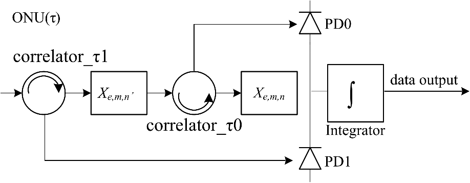
The cross-correlations of the ESP codes are specified as follows: as , , , as , , , as , or as , . Moreover, we let any two codewords ( and ), which belong to the same code group, assigned to the same user for TCK. It is set as in this letter. Table 1 uses a codeword or as the encoding of information bit “0” or “1”. The modified cross correlations in ESP codes for TCK are derived as follows: The above subtraction method for TCK can eliminate MUI according to the difference between the two correlations. For ESP scheme, we propose a new OLT as shown in Fig. 1, which includes a splitter at the remote node, and optical network units (ONUs). The AWG architecture can effectively combine all codes into one and concentrate the power. The , where , is able to decode the ESP codes to produce the information bits “0” or “1” for user(). As shown in Fig. 1, the OLT transmitter includes a broadband light source (BLS), an AWG architecture, and a matrix operation circuit. Fig. 1Schematic block diagram of extended shifted prime (ESP) codes for two-code keying (TCK) including transmitter and receiver.  The AWG architecture includes one AWG demultiplexer, electro-optic modulators (EOMs), and one AWG multiplexer. The light outputted from BLS designs wavelength bandwidth to be first divided into wavelength chips by the AWG demultiplexer. The wavelengths of wavelength chips are esignated as . These wavelength chips are then modulated by the EOMs, respectively. At last, these modulated wavelength chips are combined by the AWG multiplexer and outputted into an external fiber for data transmission. The EOM modulates the incoming wavelength chips according to the variables , which are calculated based on the information bits and adopted ESP codewords of each user via the matrix operation circuit. The calculation of this matrix operation circuit is performed according to , where , , and . Therein, and are the transpose of codeword vectors for user #0, ⋯, and and are for user #(). In fact, a universal OLT encoding architecture can be operated with other code families, e.g., SP codes and sequence codes.6,7 Only the codeword matrix needs to be updated. The proposed transmitter encodes ESP codes in the electrical domain, the same as the literature,8–11 and it has been shown that the EOM can transfer the electrical domain into the optical domain.12 In Fig. 2, the modulation voltage is the input of EOM, and the optical transmitted intensity is the output of the EOM, where the optical transmitted intensity . If , the optical transmitted intensity is . The EOM transfers the modulation voltage into optical transmitted intensity . Therefore, the ratio of transmission factor is . Figure 2 presents the transformation from the electrical domain to optical domain with the environment described in Table 1, where in ESP codes with the code weight and the code size . Fig. 2The modulation voltage versus the optical transmitted intensity of the electro-optic modulator (EOM). 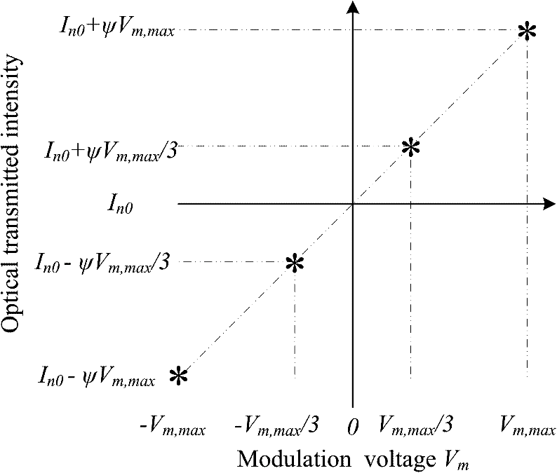 We first describe the matrix operation circuit in the electrical domain with , where , , and . The codes are then transformed to the waveform as follows. Let denote the element of . If code is transmitted and is 1, is 1/3. In contrast, if the codes and are transmitted and is 1, will be 2/3. If the codes , , and are transmitted and is 1, becomes 1. If the codes without , , and are transmitted and is 1, is 0. Let denote the maximum value of modulation voltage . Afterward, is included in the voltage setting in the transformation to the waveform, i.e., . Figure 3 shows the receiver structure of the proposed with ESP codes for TCK in an OCDMA system. The comprises two sets of fiber Bragg gratings (FBGs), one balanced detector, and an integrator. The two FBG sets are constructed based on the codewords and . The upper output part is connected to the input part of the photodetector (PD) as PD0, and the lower output part is connected to the input part of PD1.13 The balanced detector is connected to an integrator. The two cross-correlation results and lead to the output of PDs 0 to 1 in the balanced detector. The principles of the FBG-based decoder are based on the cross-correlation described as in Eq. (1). The code sequences are first received by the FBG-based decoder. Then, the signature code achieves the modified cross correlation as shown in Fig. 3. The input of the represents the spectral components. The first output of the is connected to the FBG for the code sequence . The second output of the is connected to the PD1. The spectral components with the FBG for the code sequence are reflected back toward the PD1 to obtain the photocurrent . The other spectral components are passed through the FBG for the code sequence . The other spectral components are connected to the . The first output of the is connected to the FBG for the code sequence . The second output of the is connected to the PD0. The spectral components with the FBG for the code sequence are reflected back toward the PD0 to acquire the photocurrent . The other spectral components are passed through the FBG for the code sequence . The average photocurrent is corresponding to Eq. (1). Therefore, the principles of the FBG-based decoder are based on the cross-correlation. Moreover, we eliminate the MUI with Eq. (1) according to the difference between the two correlations. Now, Table 2 compares the optical power budget for the conventional OLT using SP codes and the proposed OLT.6 Since the proposed OLT does not include splitter and combiner, which generally have high insertion loss, the power loss of the proposed OLT is much smaller than that of the conventional ones. This replaceable word is the insertion loss of A. The insertion loss of AWG is 3 dB according to the existing work.14 By contrast, the insertion losses in this paper are improved to 5 dB for the AWG multiplexer and 5 dB for the AWG demultiplexer, respectively. The total insertion loss is 10 dB. This replaceable word is the insertion loss of B and insertion loss of C. The insertion loss of AWG is 3 dB according to the literature.14 The insertion loss of AWG is 2.4 dB according to the literature.15 By contrast, the insertion losses in this paper are improved to 4 dB for the coarse AWG multiplexer and 4 dB for the fine AWG, respectively. This replaceable word is the insertion loss of D. The insertion loss of the optical switch is 0.7 dB according to the existing work.16 By contrast, the insertion loss in this paper is improved to 0.9 dB for the optical switch. This replaceable word is the insertion loss of E and insertion loss of F. The insertion loss of the optical splitter (and optical combiner) is 11 dB according to the Ref. 17. Therefore, the insertion loss is 11 dB for the optical splitter (and optical combiner). This replaceable word is the insertion loss of EOM. The insertion loss of the EOM is 1.2 dB according to the existing work.18 By contrast, the insertion loss in this paper is improved to 2 dB for the EOM. The power budget difference will be increased with the value of . Therefore, as , the optical power budget (dB) decreases from 30.9 dB in the SP codes in Ref. 6 to 12 dB in the proposed OLT. Table 2Comparison of optical power budgets for conventional OLT with SP codes and proposed OLT with ESP codes.
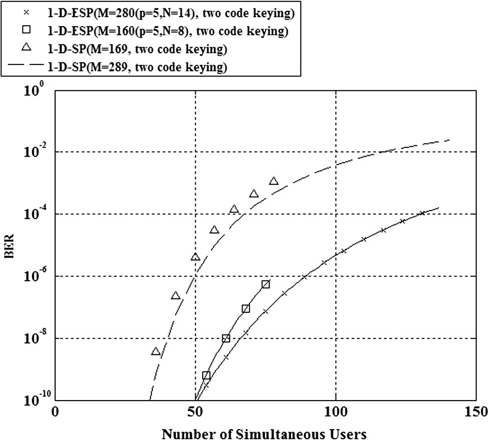
Note: Optical PB: Optical Power Budget; Code W: Code Weight; Insertion loss of: Ins.; A: 1×49 and 49×1 AWG (DE)MUX; B: 1×7 Coarse AWG; C: 7×7 Fine AWG; D: 2×1 Optical Switch; E: 1×7 Splitter; F: 7×1 Combiner. 3.System PerformanceWe first describe the signal-to-noise ratio (SNR) and bit error rate (BER) of the proposed scheme. The photocurrent noise variances are derived according to independent noise variances, i.e., and , where the average photocurrents in the received signals are , and . Note that the cross-correlation between and corresponds to the cross-correlation of the PD current and with information Therefore, if the information bit is “0,” the two cross-correlations are and . If the information bit is “1,” the two cross-correlations are and . Before obtaining , , and BER, below we first derive the number of type-I simultaneous users, probability density function of the cross-correlation value, total cross-correlation, auto correlation, and photocurrent noise variances. First, we derive the number of type-I simultaneous users. Let denote the number of simultaneous users, and we randomly choose one of them as the major simultaneous user, which selects code, whereas other () simultaneous users will select other codes. The number of type-I simultaneous users is because simultaneous users have the cross correlation as “0.” Second, we derive the probability density function of the cross-correlation value with “1” and “0.” The code weight is , and is odd. () is the even because we adopt () divided by 2 from the TCK, and the remainder is zero. The code size is in TCK. The probability density function of the cross-correlation value with “0” is . The probability density function of the cross-correlation value with “1” is . Third, we derive the total cross-correlation. Before the derivation of the PD current, the total cross-correlation is , where the cross-correlation value is “0” and “1,” the number of type-I simultaneous users is , and the probability density function of the cross-correlation value is set with “0” and “1.” Fourth, we derive the auto-cross correlation. () is the auto-cross correlation adding to the total cross-correlation. The code length () is incorporated in . The average photocurrents , and are originated as follows. For information we develop and as and . For information we develop and as and . As the information and “1,” the average photocurrent is as follows: where is the responsivity of the photodiode.Fifth, we derive the variance of the PIIN, shot noise, and thermal noise. According to the statistically independent noise characteristics, the variance of the PIIN current at each ONU receiver is as follows: where . The above equations show that the ESP codes can increase the number of simultaneous users because the variance of PIIN current is reduced by . Thus, the power of PIIN is also suppressed. Since shot noise is obtained from the mutually independent PDs 0 and 1, the variance in the shot noise current is expressed asMoreover, the variance of the thermal noise current is as Finally, we derive the , , and BER. We utilize the Gaussian approximation to find the BER, while the SNRs are and . Therefore, the BER is obtained as 6. Figure 4 shows the numerical results with , , the data , , and . The of the receiver is half of the data transmission rate. Figure 4 compares the proposed ESP codes and SP codes with similar code lengths. We use the effective source power and data transmission rate to present and 2.5 Gbps, respectively. The code weight is set as , , , and in the ESP codes for TCK. The results indicate that the maximum number of simultaneous users for and in our proposed system can reach 60 as . 4.ConclusionWe propose ESP codes and demonstrate that the effects of PIIN are effectively suppressed. Compared with the existing SP codes, our numerical results show that ESP codes can effectively increase the number of simultaneous users under 2.5-Gbps data transmission. Moreover, a universal OLT encoding architecture can be operated with other code families. Then, we also devise a AWG architecture for ESP codes to reduce the power loss and the complexity for OLT in PONs. AcknowledgmentsThe authors wish to thank the High Speed Intelligent Communication (HSIC) Research Center at the Chang Gung University, Taiwan, for providing facilities and financial support which were crucial to our study. ReferencesZ. Wanget al.,
“Optical encryption with OCDMA code swapping using all?optical XOR logic gate,”
IEEE Photonics Technol. Lett., 21
(7), 411
–413
(2009). http://dx.doi.org/10.1109/LPT.2008.2012131 IPTLEL 1041-1135 Google Scholar
H. Chenet al.,
“A tunable encoder/decoder based on polarization modulation for the SAC?OCDMA PON,”
IEEE Photonics Technol. Lett., 23
(11), 748
–750
(2011). http://dx.doi.org/10.1109/LPT.2011.2132701 IPTLEL 1041-1135 Google Scholar
V. JyotiR. S. Kaler,
“Isolated user security enhancement in optical code division multiple access network against eavesdropping,”
Opt. Eng., 51
(9), 09501
(2012). http://dx.doi.org/10.1117/1.OE.51.9.090501 OPEGAR 0091-3286 Google Scholar
B. M. GhaffariM. D. MatinfarJ. A. Salehi,
“Wireless optical CDMA LAN: digital implementation analysis,”
IEEE J. Sel. Areas Commun., 27
(9), 1676
–1686
(2009). http://dx.doi.org/10.1109/JSAC.2009.091217 ISACEM 0733-8716 Google Scholar
M. Xinet al.,
“Multipolar inserting zeros code and its application in optical code division multiple access systems,”
Opt. Eng., 46
(2), 020501
(2007). http://dx.doi.org/10.1117/1.2437123 OPEGAR 0091-3286 Google Scholar
C. C. Yang,
“Optical CDMA passive optical network using prime code with interference elimination,”
IEEE Photoics. Technol. Lett., 19
(7), 516
–518
(2007). http://dx.doi.org/10.1109/LPT.2007.893579 IPTLEL 1041-1135 Google Scholar
C.-C. Yang,
“Spectral efficiencies of the optical CDMA?based PONs using two-code keying,”
IEEE Commun. Lett., 14
(8), 767
–769
(2010). http://dx.doi.org/10.1109/LCOMM.2010.08.100585 ICLEF6 1089-7798 Google Scholar
C.-C. Yang,
“Code space enlargement for hybrid fiber radio and baseband OCDMA PON,”
Lightw. Technol., 29
(9), 1394
–1400
(2011). http://dx.doi.org/10.1109/JLT.2011.2132694 JLTEDG 0733-8724 Google Scholar
C.-C. Yang,
“Hybrid wavelength-division-multiplexing spectral-amplitude-coding optical CDMA system,”
Photonics Technol. Lett., 17
(6), 1343
–1345
(2005). http://dx.doi.org/10.1109/LPT.2005.847447 IPTLEL 1041-1135 Google Scholar
S.-M. LinJ.-F. HuangC.-C. Yang,
“Optical CDMA network codecs with merged-M-coded wavelength-hopping and prime-coded time-spreading,”
Opt. Fiber Technol., 13
(2), 117
–128
(2007). http://dx.doi.org/10.1016/j.yofte.2006.10.007 1068-5200 Google Scholar
C.-C. YangJ.-F. HuangS.-P. Tseng,
“Optical CDMA network codecs structured with M-sequence codes over waveguide-grating routers,”
Photonics Technol. Lett., 16
(2), 1041
–1135
(2004). http://dx.doi.org/10.1109/LPT.2003.823089 IPTLEL 1041-1135 Google Scholar
M. Bass, Handbook of Optics, 3rd ed.McGraw-Hill Professional(2010). Google Scholar
J. W. Goodman, Statistical Optics, Wiley, New York, California
(1985). Google Scholar
W. Bogaertset al.,
“Silicon-on-Insulator Spectral Filters Fabricated With CMOS Technology,”
IEEE J. Sel. Top. Quant. Electron., 16
(1), 33
–44
(2010). http://dx.doi.org/10.1109/JSTQE.2009.2039680 IJSQEN 1077-260X Google Scholar
K. A. McGreer,
“Arrayed waveguide gratings for wavelength routing,”
IEEE Commun. Mag., 36
(12), 62
–68
(1998). http://dx.doi.org/10.1109/35.735879 ICOMD9 0163-6804 Google Scholar
R. T. ChenH. NguyenM. C. Wu,
“A high-speed low-voltage stress induced micromachined 2x2 optical switch,”
IEEE Photonics Technol. Lett., 11
(11), 1396
–1398
(1999). http://dx.doi.org/10.1109/68.803057 IPTLEL 1041-1135 Google Scholar
Y. Hibinoet al.,
“High reliability optical splitters composed of silica-based planar lightwave circuits,”
Lightw. Technol., 13
(8), 1728
–1735
(1995). http://dx.doi.org/10.1109/50.405317 JLTEDG 0733-8724 Google Scholar
T. H. Woodet al.,
“131 ps optical modulation in semiconductor multiple quantum wells (MQW’s),”
IEEE J. Quantum Electron., 21
(2), 117
–118
(1985). http://dx.doi.org/10.1109/JQE.1985.1072626 IEJQA7 0018-9197 Google Scholar
BiographyBih-Chyun Yeh received his BS, MS, and PhD degrees in communication engineering from National Taiwan University, Taipei, Taiwan, in 1996, 1998, and 2009, respectively. He is now an assistant professor in the Faculty of Chang Gung University. His research interests include the lightwave and wireless communication systems. Cheing-Hong Lin received his BS degree in communication engineering from National Chiao Tung University, in 1997, and his MS and PhD degrees in communication engineering from National Taiwan University, Taipei, Taiwan, in 1999 and 2005, respectively. His current research interests include lightwave and wireless communication systems and computer networks. De-Nian Yang received his BS and PhD degrees from the Department of Electrical Engineering, National Taiwan University, Taipei, Taiwan, in 1999 and 2004, respectively. He is now an associate research fellow in the Institute of Information Science, Academia Sinica. His research interests include multimedia and mobile networking, social networks, theoretical rigor, and practical feasibility. |