|
|
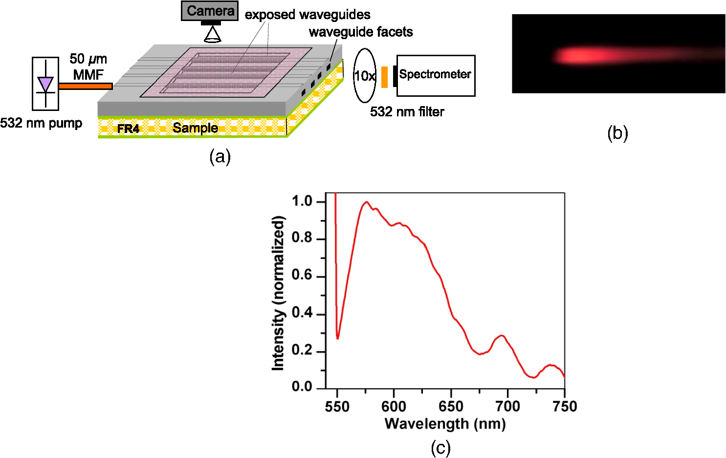
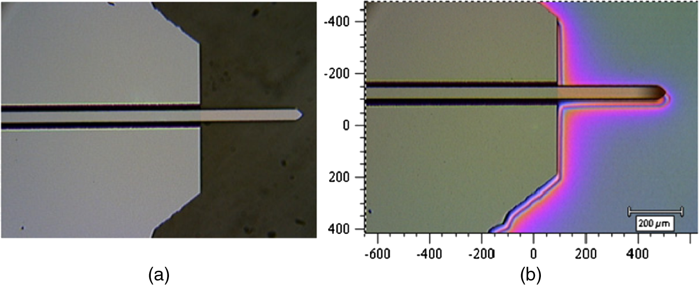
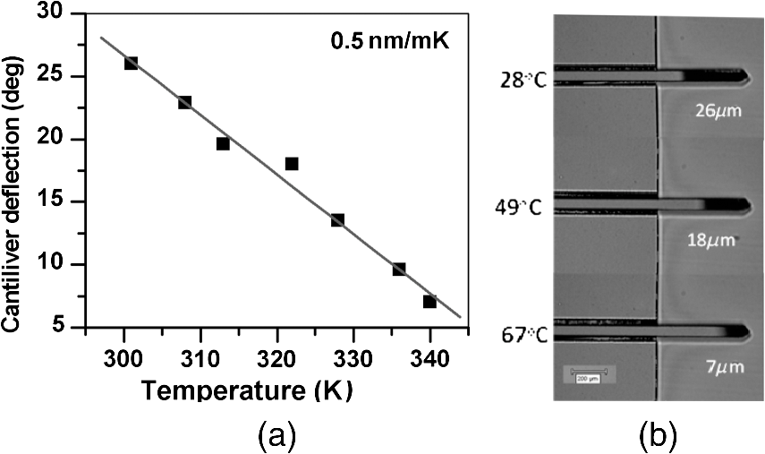
1.IntroductionWell organized, multilayered, and transparent organic–inorganic hybrid materials are an important new class of nanostructured materials.1 Such materials offer the potential for realizing a hybrid platform for the integration of optical, mechanical, and electronic devices for large number of applications, such as light sources, sensing, and data communications.2–5 When the hybridization is carried out between a glass and polymer, it offers a wide range of functionality due to the versatility of both materials in its structural, mechanical, and optical properties. Though appealing, the production of highly organized glass–polymer nanolayers is often challenging and difficult. This has been achieved via a multitarget-pulsed laser deposition (PLD) technique, which has been previously demonstrated to exhibit excellent performance for its molecular level structural engineering capabilities.6 Balancing the surface energies of both materials, glass has a surface energy at least an order of magnitude higher than polymers, is often the key aspect in this process. In this work, we plan to manage this difference by choosing a polymer with large thermal expansion coefficient (poly dimethyl siloxane (PMS) ) compared with a glass with low coefficient (tellurite glass ).7,8 Choosing a tellurite glass provides an additional advantage of large fluorescence emission bandwidth (wide tunability) and the possibility of heavy rare earth doping (high gain per unit length), facilitating the concept of optical integration at a miniaturized scale for a range of transducer materials. Hence, we have designed a superlattice of glass and polymer using a sequential PLD process.9 A 193-nm-ultraviolet (UV) laser was used to ablate the target material and the final glass and polymer superlattices were having a thicknesses ranging between 2 and 7 nm, which is within the maximum thickness 10 nm of a single layer considered in conventional crystalline superlattice. The nanolayer fabrication approach adopted for glass–polymer integration in this work for sensor applications overcomes the limitations in rare earth doping of polymer hosts. Because of the low-quantum yield doping of rare earth ions in polymer through organic complexes, such materials have not been successful in realizing practical devices so far. In our methodology, the local environment of rare earths is inorganic in nature being incorporated in the oxide glass layer and therefore the spectroscopic properties are much superior to that with an organic complex in a polymer. This is particularly important for doping with near-infrared fluorescent ions such as used in this work. Another commonly used technique to produce active functionalities based on fluorescence is to dope the polymer with dyes. Disadvantages of such dye-doped polymer systems results from the photobleaching, lack of long-term stability, and low-environmental durability. The -doped system is investigated here for potential applications in gas and chemical sensing as alternative to bromothymol blue (BTB) doping10 because of its strong-red fluorescence under green/ultraviolet excitation. In our sensor device concept demonstration, we used the -doped glass–polymer nanolayers as a composite cladding material in a planar waveguide for evanescent wave excitation and propagation. A second sensor concept demonstrated herein exploits other characteristic properties of the of the glass–polymer superlattice: (1) bending due to the internal compressive stress produced in the nanolayers of the glass–polymer superlattice deposited on to a silicon (Si) microcantilever to cause temperature dependent deflection, (2) selective, wavelength dependent differential heating of the cantilever by doping the glass layer with rare earth ion () having specific absorption at 980 nm. Such a strategy will potentially allow us to design sensor pixels for wavelength dependent imaging device of an optical-microbolometer type uncooled camera. Our approach provides the ability to fine tune the internal stress by engineering the glass–polymer nanolayers and the functionality of wavelength selectiveness by doping comparing with a previously reported approach.11 2.ExperimentalThe PDMS target materials for PLD was prepared by mixing the base and cure agents in the ratio of 10:1 of Sylgard 184 from Dow Corning, (Seneffe, Belgium). The molar percentage composition of the -doped “PT” glass targets was () (in which mol% is the total concentration of the rare earth oxides), which was prepared by powder mixing, melting, and quenching. The composition of the -doped glass target used was . The glass compositions were chosen based on their comparatively better spectroscopic properties and for their compatibility for deposition under similar atmospheric conditions as that of the polymer used. The silica substrate, used for the deposition of the superlattice structure, was cleaned and then baked inside the deposition chamber of the PLD machine (PVD Products, Wilmington, Massachusetts, USA) for degassing, prior to the deposition process. During deposition, the chamber was maintained at 5 mTorr using a gas mixture of 96% and 4% He, by volume. The deposition parameters for the formation of glassy thin films were optimized for the 193-nm-excimer laser source used, with pulse duration of 20 ns, repetition rate of 20 Hz, and fluence of . The substrate temperature during deposition was maintained at 100°C and the substrate-to-target distance during deposition was 55 mm. The superlattice like nanolayered thin films was fabricated by alternating the laser beam onto the PDMS and glass targets for ablation cycles with different durations. A preprogrammed parameter control software was used for achieving precise and frequent changeover between the two target materials. A total of 96 such cycles of 10 and 100 s for PDMS and glass were used to grow a -thick film with a glass:polymer ratio for the layers of . The duration for each target during a cycle is varied to obtain other layer thickness ratios. The very first layer deposited on the silica/polymer substrate was that of the phosphate glass (PT) glass, whereas the terminating top layer was of PDMS. After deposition the thin films were cooled to below 25°C at the rate of . A similar procedure was used to grow the -doped superlattice thin films on Si microcantilevers. 3.Nanostructure and Optical Properties3.1.Engineered StructuresThree samples were fabricated with different glass and polymer thickness ratios (, , and ) to investigate their stability and structural integrity. All structures were highly optically transparent and stable except for (3), which is disintegrated almost a week later due to very large-internal stress in the deposited film. Therefore, this particular sample was not used for any studies reported hereafter. We attribute this effect to the larger thickness of the polymer layer leading to stress relaxation over time overcoming the equilibrium force provided by the thinner glass layer. As it is evident from Fig. 1, there is a strong-contrast difference in transmission electron microscopy (TEM) images of the glass and polymer layers, which can be seen to exist in a well organized and spatially very well-defined manner. The lighter shaded layers are of low-density polymer material whilst the darker layers are that of tellurite glass with a much higher comparative density. The deposited layers have a thickness error of , which illustrates the excellent deposition quality of the layers. However, the cross-sectional area homogeneity of the layers is limited to due to particle inclusions. The formation of such particles within and its effects on the growth of the nanolayers is discussed in our previous publication.9 3.2.Optical Transmittance and Fluorescence PropertiesThe engineered superlattice films show very high transparency as shown in Fig. 2(a). The optical transmittance was well above 93% within the wavelength range of 700 to 2000 nm. Transparency is one of the major challenges in the case of organic–inorganic hybrid materials, and this plasma-based deposition technique is shown to overcome this. Two sets of films were produced, one doped with and the other doped with ions. The ions–doped film was excited using 532-nm laser and the emission was recorded in 560 to 700 nm range, and the fluorescence in this range useful for chemical and gas sensing applications where conventionally fluorescent dyes are used.10,12 The most prominent peak of the ions in films is observed at 614 nm corresponding to the to transition is shown in the spectrum normalized to this peak in Fig. 2(b). The peak at 593 nm resulting from to transition of excited ions is magnetic dipole in nature while the to transition is electric dipole in nature. This electric dipole transition is known to be highly sensitive to local coordination environment. Therefore, we can attribute the relative increase in intensity of the 593-nm peak in the normalized spectrum to the change in local coordination environment of ions in the film comparing with the target glass, which affect the electric dipole transition ( to ). The relative change in the line shapes of the two spectra are also related to the above particular properties of the two different transitions involved. For erbium-doped films, the fluorescence spectra [Fig. 2(c)] were measured from the films upon 980-nm laser excitation. : transition peaked at 1534 nm showed the almost exact line shape compared with the bulk glass and this spectrum is also shown to demonstrate absorption at 980 nm by the film. A small drop (0.2 ms) in the fluorescence lifetime for -doped superlattice in comparison to doped PT glass was observed in previous studies and discussed therein.9 On comparing the line shapes of the doped systems, we can say that there is better stoichiometric transfer of the -doped glass than -doped glass in the PLD. It is almost impossible to record the absorption spectrum with characteristic absorption features of dopants because of the low-volume fraction of the dopant ions in the thin films. The absorption of the laser will produce heating in the superlattice film due the nonradiative relaxations mainly from : to , and this aspect is utilized in the wavelength dependent deflection of the Si microcantilever in Sec. 4.2. The refractive index of the doped ( and ) superlattice structures used here were 1.635 at 633 nm, while the doped target glasses were 1.666 and PDMS was 1.454. 4.Sensor Design with Results and Discussion4.1.Europium Rare Earth Ion-Based SensorRecent advances in polymer waveguide technologies have demonstrated the potential to cost-effectively integrate optical waveguides onto standard printed circuit boards (PCBs) for use in high-speed board-level optical interconnects.13–15 However, the futher integration of optical-sensing elements onto these hybrid opto-electronic (OE) PCBs can also enable the formation of low-cost versatile optical sensors suitable for use in a variety of sensing applications.16 The selective deposition of a glass–polymer superlattice on such polymer-based devices constitutes a promising alternative in generating the required fluorescence for the sensor operation. Initial work toward this direction has been undertaken, by fabricating a waveguide sensor with a deposited glass–polymer superlattice layer. The sensor was realized by stacking a superlattice layer with selective ion doping in the glass layer, onto air-exposed channel polymer waveguides fabricated onto a standard PCB substrate. The waveguides were fabricated from siloxane polymer materials with standard photolithography techniques on a FR4 substrate. These polymer materials, OE-4140 (core) and OE-4141 (cladding) developed by Dow Corning, have been engineered to withstand the high-temperature environments in excess of 300°C, such as that are required for solder reflow and PCB lamination. The FR4 substrate constitutes a low-cost glass epoxy substrate, widely used in the electronics industry. The waveguides are designed to have a large cross section of in order to allow sensor assembly with relaxed alignment tolerances and low-cost tools such as pick-and-place machines.17,18 The fabricated sample measures and has a 10-mm long air-exposed section in order to allow the deposition of the superlattice onto the waveguides. The superlattice layers were deposited onto the waveguide sample using the PLD method discussed above. The deposition of the superlattice layer onto the exposed waveguides enables evanescensent wave coupling of the pump laser to the superlattice containing the ions and subsequently the generation of a red fluorescence signal, which is required for the sensor operation. A schematic of the fabricated device and images of parts of the sample are shown in Fig. 3. The propagation losses of the superlattice layer on silica measured at 633 nm was while the losses for polymer waveguides are below . The propagation losses are mainly contributed by the surface roughness of the film, which is typically around 90 nm for a 1-μm-thick film. Particle inclusions discussed before will also contribute to the Rayleigh scattering at the measurement wavelength. Fig. 3(a) Schematic of the printed circuit board-integrated polymer waveguide sensor with the deposited superlattice layer and (b and c) images of the fabricated sample: (b) top view of the sample edge where the deposited superlattice layer is clearly visible and (c) coated polymer waveguides in the air-exposed sensing area. 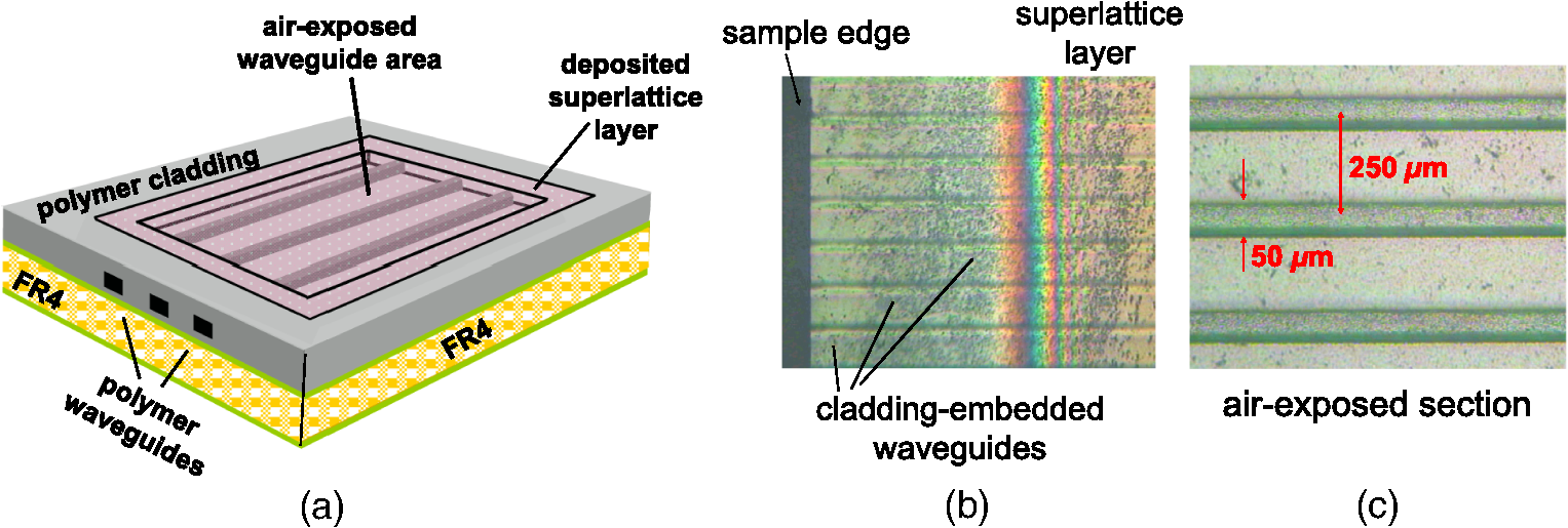 A 532-nm laser signal was lanuched into the waveguides and the europium ions in the superlattice layers were evanescently excited. Propagation of the broad amplified spontaneous emission (ASE) in the wavelength range of 570 to 650 nm is shown in Fig. 4(a) for a 532-nm laser power of 10 mW. The red color emission upon exciting the superlattice film surface is observed by the camera is shown in Fig. 4(b) while the light collected at the waveguide output clearly shows the ASE emission from the ions [Fig. 4(c)]. The ASE spectrum observed is broadened comparing with that of fluorescence spectrum reported in Fig. 2(b), which is attributed mainly to the recording of the weak evanascent signal at lower resolution. The real-time monitoring of the received fluorescense can provide information about the presence of red-absorbing chemical species in the sensor vicinity demonstrated using dye-doped waveguide systems.10 The experiments to demonstrate gas sensing are currently in progress and the integrated system requires further improvements in terms of doping concentration, transmission loss, and film thickness for optimizing the sensitivity. 4.2.Erbium Rare Earth Ion-Based SensorThe erbium ion–based sensor was designed to function as highly sensitive thermal bimorphs for unique applications, such as uncooled IR imaging devices, biological analyte microsensor, high-sensitivity thermal sensor etc. In a related experiment the ions–doped glass–polymer superlattice was stacked on a Si microcantilever, the optical image of the cantilever before and after coating is shown in Fig. 5. Due to the internal stress which is compressive in nature the cantilever bends downwards when cooled from the growth temperature down to room temperature, and with heating it deflects upward. In order to monitor the nanoscale deflection in response to low-heating temperatures a modified atomic force microscope (AFM) was configured so as to detect the deflection at a nanoscale level. The usual AFM tip-cantilever was replaced by a Si microcantilever coated with the superlattice structure directly mounted on the sample stage. The specific doping of erbium ions in glass layers enables the cantilever to absorb 980-nm laser radiation and heat the superlattice because nonradiative relaxation of ions in the glass layer from the level. The continuous wave (CW) 980-nm laser differential heating of the superlattice and silicon leads to the deflection of the bimorph cantilever. A much lower power 633-nm laser was focused on the cantilever to track the deflection; the schematic of the set up is shown in Fig. 6. Fig. 6Schematic of the experimental set up for measuring cantilever deflection using an atomic force microscope. 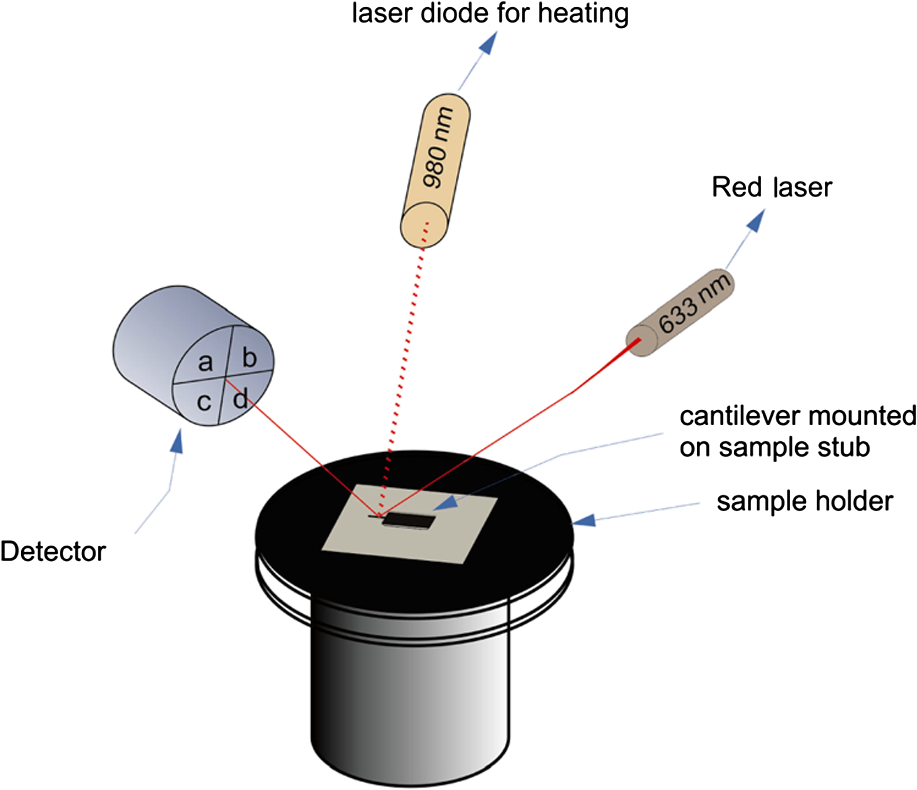 The deflection corresponding to the increase in temperature was extracted using the measured AFM and optical microscope data. A linear fit [Fig. 7(a)] was obtained for the deflection angle versus temperature graph, the slope of which was calculated to be . The corresponding images of the deflected cantilevers at selected temperatures are shown in Fig. 7(b). In this figure, we can see that the length of the cantilever under focus increases with temperature due to the upward deflection. An advantage of this biomorph methodology comparing with previous reports relying on just polymers11 is that we can design the polymer–glass interlayer thickness so as to obtain a well-controlled internal stress that can provide different levels of sensitivity. Moreover, it is possible to use the setup for monitoring wavelength dependent absorption and corresponding effects in the deflection by choosing a laser with different wavelengths or different lattice periods and materials. Since the superlattice layer can be made absorptive at wavelengths quite different from that of the underlying silicon we plan to exploit the selective heating of the glass–polymer superlattice layer for mid-IR and long wavelength detection. An array of such cantilevers can be produced on large silicon substrates for wavelength specific imaging in the long-infrared wavelength range. 5.ConclusionGlass and polymer nanolayers were engineered by PLD to produce a nanocomposite stack to thicknesses of . The thickness of the fabricated layers chosen in thus study was between 3.5 and 7 nm, and the glass layer was selectively doped with and ions for optical emission- and absorption-based integrated sensor applications. An -doped superlattice on polymer-integrated circuit platform was demonstrated as an alternative to dye-based materials for potential sensing of chemical species having absorption in the yellow–red wavelength region (590 to 620 nm). Further optimization of the doping concentrations, absorbing layer thickness, propagation losses of the evanescent wave and refractive index are required to demonstrate efficient sensing of a particular chemical species in gases or liquids. New engineering approaches for Si microcantilever-based thermal detection and imaging for optical-microbolometer/optical thermal imaging are presented and discussed. The glass–polymer superlattice approach to control the internal stress and hence to improve the thermal sensitivity together with wavelength selective detection by rare earth doping of the bimorph structure is demonstrated with high sensitivity. However, more experiments and optimization of sensitivity are required for potential device development. AcknowledgmentsAcknowledgements are due to the RCUK for the financial support for the Basic Technology Project contracts EP/D048672/1, EP/D048982/1 and DSTL-UK project MAST-STC CDE24003. The authors would like to thank Dow Corning for the provision of the siloxane polymer materials. ReferencesA. B. Bourlinoset al.,
“Layered organosilicate nanoparticles with liquid like behavior,”
Small, 1
(1), 80
–82
(2005). http://dx.doi.org/10.1002/smll.200400027 1613-6829 Google Scholar
J. ClarkG. Lanzani,
“Organic photonics for communications,”
Nat. Photon., 4
(7), 438
–446
(2010). http://dx.doi.org/10.1038/nphoton.2010.160 1749-4885 Google Scholar
C. GrivasM. Pollnau,
“Organic solid-state integrated amplifiers and lasers,”
Laser Photon. Rev., 6
(4), 419
–462
(2012). http://dx.doi.org/10.1002/lpor.201100034 1863-8880 Google Scholar
B. LebeauP. Innocenzi,
“Hybrid materials for optics and photonics,”
Chem. Soc. Rev., 40
(2), 886
–906
(2011). http://dx.doi.org/10.1039/c0cs00106f CSRVBR 0306-0012 Google Scholar
N. Martinoet al.,
“Organic semiconductors for artificial vision,”
J. Mater. Chem. B, 1
(31), 3768
–3780
(2013). http://dx.doi.org/10.1039/c3tb20213e JMACEP 0959-9428 Google Scholar
R. Eason, Pulsed Laser Deposition of Thin Films: Applications-Led Growth of Functional Materials, John Wiley & Sons, New Jersey
(2007). Google Scholar
S. M. Wiederhorn,
“Fracture surface energy of glass,”
J. Am. Ceram. Soc., 52
(2), 99
–105
(1969). http://dx.doi.org/10.1111/jace.1969.52.issue-2 JACTAW 0002-7820 Google Scholar
R. El-Mallawany,
“Tellurite glasses: Part 2. Anelastic, phase separation, Debye temperature and thermal properties,”
Mater. Chem. Phys., 60
(2), 103
–131
(1999). http://dx.doi.org/10.1016/S0254-0584(99)00082-6 MCHPDR 0254-0584 Google Scholar
Z. Zhaoet al.,
“Active glass-polymer superlattices for photonic integration,”
Nanotechnology, 23
(22), 225302
(2012). http://dx.doi.org/10.1088/0957-4484/23/22/225302 NNOTER 0957-4484 Google Scholar
N. Bamiedakiset al.,
“Low-cost PCB-integrated polymer waveguide sensor for gas detection,”
in CLEO: 2011—Laser Applications to Photonic Applications. CThC5,
(2011). Google Scholar
M. C. LeMieuxet al.,
“Polymeric nanolayers as actuators for ultrasensitive thermal bimorphs,”
Nano Lett., 6
(4), 730
–734
(2006). http://dx.doi.org/10.1021/nl0525305 NALEFD 1530-6984 Google Scholar
S. T. Leeet al.,
“A sensitive fibre optic pH sensor using multiple sol-gel coatings,”
J. Opt. A: Pure Appl. Opt., 3
(5), 355
–359
(2001). http://dx.doi.org/10.1088/1464-4258/3/5/307 JOAOF8 1464-4258 Google Scholar
R. Dangelet al.,
“Polymer-waveguide-based board-level optical interconnect technology for datacom applications,”
IEEE Trans. Adv. Packag., 31
(4), 759
–767
(2008). http://dx.doi.org/10.1109/TADVP.2008.2005996 ITAPFZ 1521-3323 Google Scholar
M. ImmonenM. KarppinenJ. K. Kivilahti,
“Fabrication and characterization of polymer optical waveguides with integrated micromirrors for three-dimensional board-level optical interconnects,”
IEEE Trans. Electron. Packag. Manuf., 28
(4), 304
–311
(2005). http://dx.doi.org/10.1109/TEPM.2005.856538 ITEPFL 1521-334X Google Scholar
N. Bamiedakiset al.,
“Cost-effective multimode polymer waveguides for high-speed on-board optical interconnects,”
IEEE J. Quantum Electron., 45
(4), 415
–424
(2009). http://dx.doi.org/10.1109/JQE.2009.2013111 IEJQA7 0018-9197 Google Scholar
N. Bamiedakiset al.,
“PCB-integrated optical waveguide sensors: an ammonia gas sensor,”
J. Lightwave Technol., 31
(10), 1628
–1635
(2013). http://dx.doi.org/10.1109/JLT.2013.2255582 JLTEDG 0733-8724 Google Scholar
N. Bamiedakiset al.,
“Low-cost PCB-integrated 10-Gb/s optical transceiver built with a novel integration method,”
IEEE Trans. Compon. Packag. Manuf. Technol., 3
(4), 592
–600
(2013). http://dx.doi.org/10.1109/TCPMT.2013.2242961 2156-3950 Google Scholar
I. Papakonstantinouet al.,
“Low-cost, precision, self-alignment technique for coupling laser and photodiode arrays to polymer waveguide arrays on multilayer PCBs,”
IEEE Trans. Adv. Packag., 31
(5), 502
–511
(2008). http://dx.doi.org/10.1109/TADVP.2008.924243 ITAPFZ 1521-3323 Google Scholar
BiographyTarun Kakkar finished his master’s degree in pharmaceutical science and engineering from University of Leeds in 2011. He has worked as a research assistant in the Institute for Materials Research, University of Leeds, where he is currently pursuing his PhD in materials science. He is involved in integrating tissue engineering with nanotechnology in building noninvasive techniques for medical diagnostics. Nikos Bamiedakis received his diploma degree in electrical and computer engineering from National Technical University of Athens (NTUA), Athens, Greece, in 2003 and a PhD in engineering from the University of Cambridge, Cambridge, UK, in 2008. Since then, he has worked as a research associate at the University of Cambridge. His research focuses on optical waveguides and waveguide components for high-speed board-level optical interconnects and optical sensing applications. Toney Teddy Fernandez received his PhD degree from Mahatma Gandhi University (India). He is currently working as a senior postdoctoral fellow at Instituto de Optica, CSIC, Madrid. His major research focus is on materials processing with ultrafast lasers. He has previously worked at Politecnico di Milano, Italy, and University of Leeds, UK. Zhanxiang Zhao received her PhD degree in materials engineering in 2012 from University of Leeds under the supervision of Professor Animesh Jha. Her research was focused on fabrication and characterization of glass–polymer composite thin film grown by pulsed laser deposition and fabrication of nanoscale devices using photolithography followed reactive ion etching in the cleanroom. Mehrdad Irannejad received his bachelor’s (Shiraz University, Iran, 2000) and master’s degrees in physics (Shiraz University, Iran, 2003) and nanoelectronic and photonic components engineering (University of Leeds, UK, 2008). He received his PhD from the University of Leeds in 2012. From 2003 to 2007, he was a physics instructor at Yasouj University, Iran. His research interests include engineering surface plasmon sensors, ultrafast graphene electronic devices, engineering of laser hosts, glass-semiconductor integration, thin film, pulsed laser deposition, and biophotonics. Paul Steenson received his BSc degree from the University of Manchester in 1984, and his PhD from the University of Nottingham in 1993. From 1984 to 1986, he worked at Philips Components-UK and Philips Research Laboratories-UK. After a short period at the University of Nottingham he joined the University of Leeds where he is a senior lecturer with research interests in microfabrication and integration of novel millimeter- and submillimeter-wave devices and circuits and pulsed laser deposition. Animesh Jha received his bachelor’s (University of Roorkee, India, 1979) and master’s degrees (IISc, Bangalore, India, 1981), and his PhD degree (1984) from Imperial College London, U.K. He was a research fellow at the University of Sheffield until 1989, after which he was appointed lecturer at Brunel University. In 1996, he joined the University of Leeds, U.K., where he is a professor of materials science. His research interests include engineering of laser hosts, glass-semiconductor integration and biophotonics. Richard Penty received his PhD in 1989 from Cambridge University. He returned to Cambridge in 2001, having been a professor at the University of Bristol. He has been an author of in excess of 750 refereed journal and conference papers and is editor-in-chief of IET Optoelectronics. He is a cofounder of Zinwave, a fellow of the Royal Academy of Engineering, a fellow of the IET and Master of Sidney Sussex College. Ian White is currently master of Jesus College, van Eck Professor of Engineering, deputy vice-chancellor and head of research at the Department of Engineering, University of Cambridge. He gained his BA and PhD degrees from the University of Cambridge in 1980 and 1984. He is a fellow of the Royal Academy of Engineering, the Institution of Electrical Engineers and the IEEE. He has published in excess of 900 journal and conference papers. Gin Jose received his MSc and PhD degrees in physics from University of Calicut, India and Mahatma Gandhi University, India, in 1996 and 2003, respectively. He was a research fellow at the Politecnico di Milano (2001 to 2002). In 2003, he joined the Indian Institute of Technology Guwahati as senior lecturer and he was an assistant professor there from 2004 to 2007. In 2007, he moved to the University of Leeds, where he is currently the chair in Functional Materials. |