
|
|
1.IntroductionThe success of optical fibers for lightwave communications, employing silica (i.e., amorphous ) as base material, has paved the way to a large use of optical glasses in photonic applications and, in particular, integrated optics (IO). The field of IO had been conceived in 19691 to complement the passive transmissive medium (i.e., the optical fibers) with integrated chips, where all the active (signal generation or amplification) and passive (signal addressing and processing) functions could be performed via the guided propagation of light. Since then, much activity has been carried out to develop what we can also refer to as photonic integrated circuits (PICs); an interesting overview was published some years a ago by Kaminow, who had been member of the Bell Labs’ group which was pioneering in this area.2 Many optical materials are currently employed in the fabrication of PICs, but glass remains a fundamental one. Novel glasses and/or fabrication processes have obviously been developed to respond to the growing new requirements, and glass IO now constitutes a branch of photonics capable of offering sophisticated and innovative solutions to many problems—yet involving rather simple technologies. Integration was the keyword in the seminal paper by Miller;1 even today, however, the goal of a full monolithic integration, possible in semiconductor materials, does not always represent the best solution, while hybrid integration often permits to take advantage of the complementary characteristics of the different classes of materials needed in IO (namely, semiconductors, ferroelectrics, glasses, and polymers). Thus, glassy materials keep offering many useful characteristics such as relatively low cost, excellent transparency, high threshold to optical damage, a relatively wide interval of refractive indices to choose from, and, last but not least, the easiness of doping with active and functional atoms and oxides. Glass is also a fundamental component of the main technological platforms for PICs, namely silica-on-silicon (SOS) and silicon-on-insulator (SOI). Optical waveguides (WGs) are the building block over which PICs are designed and fabricated; this paper presents a brief overview of a number of different processes suitable for the fabrication of glass WGs. As to the material itself, pure glasses are the most popular material for the fabrication of passive components, but extended the functionality can be easily achieved by doping the glass matrix with proper ions, elements, or compounds. This aspect is also briefly considered in the following. 2.Thin Film Fabrication ProcessesGlass WGs exhibit very good properties, owing to the relatively simple technology, the low propagation losses, and the easy matching to glass fibers. The availability of low-loss glasses and cheap and reliable WG fabrication techniques has been of major importance. A general requirement is that the fabrication technologies must—first of all—be capable of high yield, with assured reproducibility within the specified tolerances, and of intrinsic low operation cost. In the case of glass IO, the most usual WG fabrication techniques can be classified according to the scheme in Fig. 1. Since the most basic requirement for confining the light is that the guiding layer has a refractive index (RI) higher than the surrounding media, two major approaches can be followed: (a) deposition of a thin film and (b) local modification of the bulk material. The former approach includes processes such as radio frequency (RF) and magnetron sputtering, chemical vapor deposition (CVD, and in particular plasma-enhanced chemical vapor deposition—PECVD), flame hydrolysis deposition (FHD), spray pyrolysis (SP) deposition, pulsed laser deposition (PLD), sol–gel coating; the latter approach, which is also suitable to the direct definition of a channel WG, includes ion exchange, ion implantation, UV irradiation, and femtosecond laser writing. All the above processes may then be followed or complemented by other ones such as annealing, photolithography, and etching. Fig. 1Fabrication techniques of glass optical waveguides (WGs) can be classified in two major categories: one refers to thin film deposition techniques, either physical or chemical, and the other concerns process for local modification of the refractive index of the glass, either in bulk or thin film format.  It has to be remarked that none of the fabrication techniques indicated in Fig. 1 is peculiar to glass IO only: they are largely used in a wide range of application areas, from thin-film coatings to microelectronics, material processing, and glass strengthening. Indeed, some of these techniques, like resistive evaporation, are rarely used for the fabrication of WGs, being, on the contrary, a standard method of producing thin metal films and, as such, largely used to produce the metal layers needed in the patterning processes of IO circuits and for electrical contacts. Electron-gun evaporation would be more effective, but it too has not been frequently used for optical WGs. Another technique cited in Fig. 1 but not so common in IO is SP: it is a process in which a thin film is deposited by spraying a solution on a heated surface, where the constituents react to form a chemical compound.3 It involves three main steps: atomization of the precursor solution, transportation of the resultant aerosol, and decomposition of the precursor on the substrate, with final sintering of the solid particles. SP is suitable to prepare dense and porous oxide films, ceramic coatings, and powders. An advantage of SP is that it does not require high quality substrates or chemicals. Films prepared by the SP have been used in various devices, such as solar cells, sensors, antireflection coatings, thermal coatings, solid oxide fuel cells, and many others; as an example, rare-earth-doped Al2O3 films prepared by the SP have shown efficient blue-green luminescence and white light emission.4 Let us now briefly consider the most common deposition techniques for glass optical WGs. 2.1.Pulsed Laser DepositionPLD, namely thin film deposition by laser ablation from a target material, is a technique in use since the end of the 1980s, which proved to be effective for depositing high-quality optical films.5 PLD has a high potential to produce complex high-quality glassy films for integrated optical applications. Its main advantages over other deposition methods are the capability of producing glassy films in an extended compositional range with respect to bulk materials, the possibility of avoiding oxygen deficiencies in the glass network by using an oxygen pressure during deposition, the capability of producing complex oxide hosts and the possibility of incorporating controlled structure nanoparticles. PLD has also been used to produce thin films with high erbium ion concentration from bulk phosphate,6 tellurite, phospho-tellurite, and chalcogenide glasses.7,8 As an example, high-quality phospho-tellurite thin films up to 2-μm thickness with propagation losses were deposited using a 193 nm ArF excimer PLD system in a low pressure oxygen atmosphere.8 2.2.Sputtering DepositionSputtering is one of the most popular techniques, in the category of physical deposition processes, for producing low loss and even complex glass WGs. Some of the earliest glass WGs, made of Corning 7059 glass, were fabricated by sputtering.9 Sputtering is based on the use of positively charged highly accelerated ions to eject particles—usually atomic clusters or neutral atoms—from a target made of the material to be deposited. Most of the ejected particles then strike the substrate and adhere to it, so that a high-quality film is gradually built up. The sputtered films are generally more dense than evaporated films,10 but less dense than pulsed-laser-deposited films.11 The accelerated particles may be created in a glow discharge plasma of an inert gas (usually argon) or by an ion beam. The physics of sputtering is quite complex, and the interested reader is referred to some of the many review articles and textbooks on this topic.12 The sputtering yield is defined as the ratio, in a given time, of the number of particles sputtered to the number of incident particles. The sputtering yield increases with the angle of incidence of the accelerated ions, and it is dependent upon the energy of the incident particle and on the nature of the particle and of the target to be sputtered. The simplest sputtering system is a planar “diode” system, where a potential difference is maintained between a cathode (the electrode with which the target to be deposited is in contact) and an anode (usually electrically grounded), on which the substrate is placed. Although a metal target can be easily sputtered by applying a direct current (dc) voltage, for the sputtering of an insulating material (such as silica), an RF discharge (usually at 13.56 MHz frequency) is adopted to avoid the accumulation of negative electrical charges onto the target. More recently, the magnetron configuration has often been used with permanent magnets placed below the cathode: when a magnetic field is coupled with the sputtering source, it traps electrons close to the target surface and hence decreases their mean free path in the plasma. More ions are thus created by impact with electrons close to the target and this lead to higher sputtering rates. Sputtering is a relatively slow process, with deposition rates of the order of a few nanometers per hour per Watt of RF electric power applied to the electrodes. In typical working conditions, the pressure of the sputtering gas is of the order of , and the electric power is in the range of 200 to 300 W. The quality of films is generally quite good, with propagation losses repeatedly . Composition and RI of sputtered films vary as a function of the power level and/or the gas pressure at which the deposition is made. Neither compounds nor alloys are removed from the target in their combined or associated state: the material is often sputtered as a range of atoms and fragments of the original molecule, so that the compound must reform on the substrate. Thus, when sputtering oxide glasses, there is a good likelihood of loss of oxygen caused by the dissociation of glass during the collisions of ions onto the target.13 In order to reduce these effects, a percentage of oxygen can be introduced in the plasma (reactive sputtering) and a little potential can be applied to the anode (bias sputtering). In order to reduce optical losses, a thermal annealing process is often necessary; annealing, in fact, reduces losses by oxidizing the sputtered material and homogenizing the deposited thin film by enhancing the diffusion process.14 Magnetron sputtering, in particular, appears to be a valuable alternative to other WG fabrication processes; high-quality films have been produced, for instance, for light amplification, due to doping with rare-earth15–17 and biosensing.18 It is worth of notice the fact that the two latter devices use chalcogenide glasses, so showing a viable approach to the development of glass IO for mid-IR. 2.3.CVD and FHDThe CVD method19 was originally developed for the production of preforms of optical fibers, but it can be advantageously applied to planar WGs as well. In the latter case, CVD is employed to create thin films of a material on a substrate via the use of chemical reactions. Reactive gases are fed into a vacuum chamber and these gases react on a substrate and form a thin film or a powder. In classical CVD equipment, the silica (or silicon) substrate is placed in a reaction chamber, where accurately controlled flows of oxygen (carrier gas) and reactant gases (such as , , and ) are introduced. Depending on the process and operating conditions, the reactant gases may undergo homogeneous chemical reactions in the vapor phase before striking the surface. The gaseous by-products of the reaction are transported out of the reaction chamber. Referring to the above gases, the reaction with oxygen at a temperature causes the reagents’ oxidation and the deposition of a thin oxide layer (with composition) onto the substrate. The WG is then obtained by vitrification of the soot at a temperature around 1700°C; a lower-index cladding layer can also be deposited on the WG by reducing the flowing rate of . The resulting CVD-deposited glass films usually show absorption loss at 632.8-nm wavelength. Low-loss rib or channel WGs can also be formed by this technique, through the use of suitable etching processes. The CVD process lends itself to many modifications, which have been developed in different laboratories with the aim of optimizing both the quality and the yield of the process. The most common types of CVD-derived fabrication techniques used to make IO devices include FHD,20,21 low pressure CVD (LPCVD),22 PECVD,23,24 and atmospheric pressure CVD (APCVD)25,26 processes. FHD likely is the most economical technique for the deposition of films, exploiting the hydrolysis of in a high temperature flame. Even if the precise control of deposition and stoichiometry is quite difficult, and an additional process of densification of the porous soot into dense film is necessary, FHD is extensively employed to deposit thick amorphous silica films due to the high deposition rate and high material quality.21 The flexibility of this technology, however, has allowed to successfully adopt it for various applications, like optical biochemical sensor arrays, integrating optical, and microfluidic circuitry.27 LPCVD can only be performed at high temperatures, and its low rate of the reaction allows us a greater control over film thickness and uniformity, also improving films purity. In the case of composite glasses, like borophosphosilicates, the choice of the source materials may also be important for a better control of the film properties.22 The simplicity of the process permits the processing of large wafer batch sizes. PECVD permits energetic reactions at low temperatures (even 100°C in some cases), due to the formation of cold plasma by electrical ionization rather than thermal ionization.23 The process is more complicated than LPCVD and therefore is less suitable to large batches. It is, however, very frequently used for the deposition of low-loss silica and silica-germanate WGs.28 Further developments have made possible to effectively avoid problems which can occur when fabricating dense WG arrays, like the creation of voids during the deposition of the upper cladding. An improved process, for instance, that uses boron–germanium codoped upper-cladding and high-temperature annealing has produced a low-loss cross-order arrayed-waveguide-grating (AWG) triplexer used as test device.29 APCVD is attractive for both economic and technological reasons, particularly due to the online-processing capability, which substantially reduces substrate handling cost.26 It is often applied to the deposition of passivation layers in the semiconductor manufacturing process, but can also be employed in IO, due to the advantage of low temperature treatment, which is effective for minimizing film stress and therefore producing low-birefringence WGs. As an example, APCVD was applied to the fabrication of a frequency division multiplexer and of a Mach–Zehnder interferometer; the latter one was used to test the photosensitivity of guiding structures based on phosphorous-doped silica glass cladding and codoped germanium and phosphorous silica core.25 2.4.Sol–Gel DepositionA low cost and versatile approach for the realization of glass and glass ceramic (GC) WGs is based on sol–gel route. This method exploits chemical reactions of a main precursor, generally an organometallic compound in alcoholic solutions.30 From an historical point of view, even if the synthesis of the first silica gel dates back to 1846,31 sol–gel chemistry has been investigated extensively only since the mid-1970s, when sol–gel reactions were shown to produce a variety of inorganic networks that can be formed from metal alkoxide solution. Here, we will focus on the metal–organic route with metal alkoxides in organic solvent,32 which offers unique opportunities for the synthesis of optical materials in different forms such as fine powders, monosize nanoparticles, aerogels, xerogels, and WGs, as represented in the simple diagram of Fig. 2. Another possible approach is to follow the inorganic route with metal salts in aqueous solution:30 it has the advantage of being much cheaper than using metal alkoxides, but the control of the reactions is more difficult. Fig. 2Sketch of the sol–gel synthesis processes of optical glassy materials in different forms, such as monosize nanoparticles, aerogels, and xerogels, in thin film or bulk format.  As shown in Fig. 2, the sol–gel chemical process is self-described in the definition of a sol, a gel, and a summary of the processes in which the sol evolves into a gel. The main reactions involved in the sol–gel chemistry are based on the hydrolysis and condensation of metal alkoxides, which can be outlined as shown in Fig. 3. Fig. 3Summary of the main reactions involved in the sol–gel chemistry based on hydrolysis and condensation of metal (M) alkoxides (OR). OH indicates the hydroxyl group. 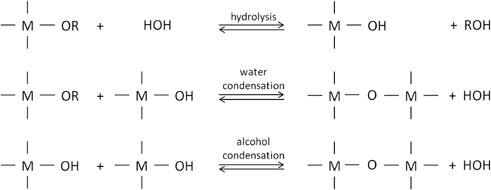 In the first step, the hydrolysis reaction, due to a nucleophilic attack of water to the metalloid atom, allows the substitution of the alkoxide groups (OR) with the hydroxyl groups (OH). In the second step, the condensation reaction brings to the constitution of the amorphous network M–O–M with the elimination of water and alcohol. Due to the fact that the hydrolysis kinetic in a neutral environment is very slow, generally it is preferable to make the reaction happen in acid or basic catalysis. Because of the presence of a lot of chemical reactions and several involved compounds, the thermodynamic and kinetic description of the process result to be very complex; the main parameters that affect the reactions are the water-to-alkoxide ratio, the type and amount of catalyst, the type of organic groups attached on M (metallic) atom, and the solvent. All these conditions should be considered in order to create a stable suspension necessary for the realization of efficient optical devices. Other aspects concern the form of the final material: the precursor sol, in fact, can be either deposited on a planar substrate to form a film (WG), e.g., by dip-coating or spin-coating, or can be cast into a suitable container with the desired shape (xerogel), or it can be used to coat substrates with nonplanar shape. A limitation to the film deposition is the time length of the process: due to the risk of stress cracking, that is, a result of the reduction of volume of the deposited layer during the drying process, generally it is impossible to deposit films with thickness in a single step. Several deposition/heating cycles are, therefore, necessary to achieve films with a thickness suitable for an optical WG. Viscosity of the solutions, deposition parameters (dipping rate for dip-coating process and rotation speed for spin-coating one), and postdeposition heat treatment (HT) conditions are crucial aspects that have to be calibrated for each material. Silica-based WGs are mostly produced by using alkoxysilanes, such as tetramethoxysilane and tetraethoxysilane; the acid nature of the catalyst permits to obtain a material with high uniformity, low porous volume, and high density, fundamental properties for the development of photonic devices. A complementary approach uses organic–inorganic hybrid materials (e.g., hydrogen silsesquioxane, 3-glycidoxypropyl-trimethoxysilane) as starting reagents; in this case, the removal of the organic part occurs using HT process at high temperature. In all materials obtained by sol–gel route, the HT process is critical for the densification of the structures: HT, in fact, permits not only the stiffening of the network, but also the removal of hydroxyl groups () that are one of the main causes of absorption in the near-infrared and of the luminescence quenching for rare-earth ions, especially erbium ions. Finally, playing with HT, it is possible to pass from an amorphous matrix to a GC system, usually exhibiting better characteristics (see Sec. 3). Literature is rich of papers where the sol–gel route has been used for the realization of planar WGs with low propagation losses (better than at 1.5 μm)33 and for the fabrication of integrated optical devices such as monolithic lasers34 and optical sensors.35 The choice of a suitable precursor is also fundamental for achieving WGs with low losses. Many precursors can be used, typical reagents being salts,36 alkoxides,37 and oxysalts.38 Another aspect that must be considered concerns the total molar concentration of the sol, which also plays an important role in the formation of a matrix with very low defects and good intermingling of the network. In particular, it has been demonstrated that a high total molar concentration yields a more viscous sol, but the final film presents a lower intermingling of the network, thus being less suitable for good WGs. A typical value of total molar ratio that permits one to obtain high optical quality films is about .39 As previously mentioned, the fabrication of an optical WG requires a sequence of deposition/heating cycles; if we consider a guiding film with a RI of about 1.57 at 1.5 μm, the minimum thickness needed to support one mode at this wavelength is around 1 μm. Referring to the dip-coating approach, a reasonable withdrawing rate is about : this value permits to deposit a layer thick some 30 nm for each cycle, so that 35 dips are necessary to obtain the required 1 μm film. Typical HT condition after each deposition cycle is 900°C for about 1 min, but the temperature and duration of HT strongly depend on the nature and molar composition of the binary system; for instance, in silica–tin oxide or silica–titanium oxide layers an HT of 900°C for 50 s may induce phase separation in the system and create nanocrystals (of or , respectively) with the size around 4 to 5 nm, while in silica–hafnia or silica–zirconia, the same HT does not produce any phase separation.40 The final HT has also to be optimized according to the molar ratio of the binary systems. As an example, in silica–hafnia or silica–zirconia films with different molar ratios (i.e., , , , where or Zr) the HT time has to be decreased when the molar content of is increasing. Typical duration of HT at 900°C in order to achieve full densification is around 5 min for the 70:30 composition, 3.5 h for 80∶20 and 30 h for 90∶10.41 On the other hand, increasing the temperature above 900°C (e.g., 1000°C) produces phase separation with the formation of nanocrystals, thus creating a GC matrix. 3.Glass Ceramic WaveguidesGCs may be defined as polycrystalline materials produced through controlled crystallization of base glass; they share many properties with both glasses and ceramics and can be considered as a class of nanocomposite materials, that is of those materials whose structural elements (clusters, crystallites, or molecules) have dimensions in the 1 to 100 nm range.42 Applications of GC in optics date back to 1968, with the development by Schott of Zerodur®, which has been largely used as low-thermal-expansion substrate of telescope mirrors.43 More recently, huge advances have been made both in the synthesis of size-tunable, monodisperse nanoclusters of various chemical compositions and in the development of techniques for their assembly into well-ordered nanostructured solids facilitating the synthesis of what are often termed designer materials. The importance of GC for the development of photonic devices appeared clear in the nineties, when one of the pioneering works was published by Wang and Ohwaki.44 Another important step was made in 1998 when it was demonstrated that subdecibel per kilometer loss could be achieved in Tm-doped fluoride optical GC fibers.45 GC WGs are produced by a suitable thermal treatment; laser annealing too may be quite effective.46 They are characterized by high transparency in the cerammed state and by the fact that rare-earth dopants are preferentially incorporated into the crystals, so that the emitting ions experience a lower phonon energy environment than in the glass matrix. The propagation losses of GCs depend, as usual, on absorption and scattering: absorption can generally be reduced to acceptable levels by purification of the starting materials and by careful melting practices; scattering, on the contrary, is not easily eliminated in glasses, and a general theory describing the relationship between structure and transparency in GCs is still under investigation.45,47 From an experimental point of view, four criteria must be fulfilled for a GC material in order to be suitable for optical waveguiding: particle size must be smaller than 15 nm (for visible light); interparticle spacing must be comparable with the crystal size; particle-size distribution must be narrow; no clustering of the crystals should occur. As an example, high-quality GC WGs may be easily produced by suitably processing the matrix; for a molar concentration of below 30%, the matrix remains amorphous if treated at 900°C, but an annealing at 1000°C for 30 min is sufficient to produce the formation of nanocrystals.48 In these conditions, it is possible to obtain a nanostructured system fulfilling the three conditions to achieve low-losses WGs: (i) nanocrystals (NCs) that present low size (4 to 6 nm), (ii) NCs with narrow particle-size distribution, and (iii) NCs homogeneously dispersed in the amorphous matrix. GCs have thus proved to be one kind of the most promising materials for the fabrication of photonic devices like optical amplifiers, tunable solid-state lasers, luminescent solar concentrators and up-conversion luminescence devices.49,50 A number of papers, in particular, deals with planar and channel WGs; some examples refer to: (i) optical WGs produced by ion exchange in electro-optical GCs, demonstrating a high Kerr coefficient51 and (ii) WGs realized using sol–gel route, presenting low attenuation coefficient at 1.5 μm and suitable for single band amplification in the C band of telecommunications.52–55 4.Local Modification of Optical PropertiesOptical WGs can also be produced by varying the RI of the bulk material, either by diffusion processes (at low energies: ion exchange; at high energies: ion implantation) or by selective irradiation by a light beam (UV or fs-laser writing). In this section, the main characteristics of these processes will be summarized. 4.1.Ion ExchangeIon exchange is a very old process that is based on the substitution of an ion already present in the glass (usually ) with another ion (e.g., , , and ) supplied from an external source (usually a salt melt).56 As a technique to color glasses, it dates back to the first millennium: it appears that Egyptians already used it in the sixth century to decorate dishes and pots in brownish yellow. A few centuries later, the Moors used this technique to stain the window glass of their palaces in Spain. The strengthening of glass surface by ion exchange (IE) became a standard industrial process in the 1960s. The suitability of IE technology to produce optical WGs in glass has been recognized since the early 1970s, when the pioneering works of Izawa and Nakagome57 and Giallorenzi et al.58 demonstrated the way to take advantage of the RI increase in IO, which is produced by the substitution of the sodium ion with another ion having higher electronic polarizability, such as silver. Different ion exchanges, e.g., with Ag, K, Cs, Rb, and Tl ions, have been investigated, and these processes have been extensively used for the fabrication of graded-index optical planar and channel WGs and IO components. Both ion diffusion from molten salt baths and the electro-migration of a metal film deposited onto the sample surface have been exploited. Some excellent review papers are available, and the reader is referred to them for an overview of the different processes and models.59–61 Ion exchange produces graded-index WGs, and one of the critical issues in this area concerns the accurate determination of their RI profile. The most common method in IO is to reconstruct the RI profile starting from the experimental measurement of the synchronous coupling angles (i.e., the angles at which the light from a laser source is coupled into the WG modes). In fact, that knowledge is fundamental to proper designing of IO components and to minimize the insertion loss of any graded-index planar IO device. Different numerical methods and computational algorithms have been thus developed and tested for the index profile modeling; commercial software is now available for index profiling and simulation of the optical guided propagation. It is interesting to note that the analysis of the same ion-exchanged WGs in different laboratories did not give completely uniform results.62 On the fabrication side, it is quite obvious that one of the greatest advantages of the IE technique stays in the simplicity of the process, with its low cost and convenience for large-batch production. The simplest laboratory equipment for IE only requires an oven where the vessel (usually in stainless steel or fused quartz) containing the salt can be placed and then the sample is dipped in the molten salt. The only critical issue may be the accurate control of the temperature of the salt melt during long exchange processes. Planar and channel WGs are easily and consistently fabricated.60 A systematic study of thermal IE used for the fabrication of optical channel WGs in a single-alkali glass was published by Li et al.63 The burial of channel WGs is of particular interest in order to achieve a more symmetrical modal field, and therefore an efficient matching to modal field of input/output fibers. Simple thermal annealing after IE may be useful, but the best results are obtained through field-assisted processes.64,65 In the latter case, the experimental apparatus is a bit more complex because of the problems related to electrical contacts on the sample and the need for electrical insulation between cathode and anode (which are often the molten salts themselves). Moreover, since IE in glass allows manufacturing either surface or buried WGs, this technology is well adapted for three-dimensional (3-D) integration of passive and/or active devices provided that any parasitic light transfer between the two layers is avoided. The feasibility of this approach has been demonstrated by using thermal IE for the surface WG and thermal plus field-assisted IE for the deeply buried one.66 So many IO devices have been fabricated so far by using IE that it would be impossible to enlist them; let us just make the reference to a few of them, starting from pioneering works on WG lasers,67 arrayed waveguide gratings (AWG),68 add-drop filters,69 lossless or amplified splitters/combiners,70,71 up to WG laser arrays.72–74 4.2.Ion ImplantationIon implantation is a high-energy process that is often used in the semiconductor industry and is becoming more and more common in IO as well. In this process, a beam of atoms is ionized, accelerated to kinetic energies up to several MeV, and aimed at a suitable material target. A great advantage of ion implantation is that virtually any element can be inserted in the near-surface region of any solid substrate. When an energetic ion is implanted into a material, it looses its energy by electronic and nuclear damage. The nature of the process is quite complex and the interested reader is referred to one of the many books on the subject.75,76 Implantation in dielectric materials, however, is always producing a change in RI; depending on the process and the material, the change can be positive or negative. Often most of the damage occurs at the end of the ion track inside the substrate, which results in a volume expansion with consequent decrease of the physical density and decrease of the RI. An optical barrier is thus created that permits the confinement of light in a narrow layer between the substrate’s surface and the barrier. This confinement can be rather weak and a so-called tunneling effect may take place, with leakage of energy of the propagating beam. In some cases, however, the RI might first experience a positive change in the main region of the ion range, forming an enhanced index well, which provides better confinement. Accordingly, the confinement structure of ion implanted WGs can be divided in two types: “barrier” and “.” The penetration depth profile of the vacancies produced by the ion beam is generally calculated with the Stopping and Range of Ions in Matter (SRIM) code.77 Optical WGs have been fabricated by ion implantation in more than hundred optical materials, including crystals, glasses, and polymers,78,79 and also materials where other techniques failed, as tellurite glasses.80,81 Early attempts to use ion implantation for glass WGs had been made by bombarding silica substrates with ions accelerated at 1.5 MeV82 and with ions accelerated at 32 to 200 keV.83 Figure 4 shows a graphical comparison of 3.5 MeV implanted distribution in an -doped tungsten tellurite glass as obtained by SRIM with the barrier layer boundaries obtained by spectroscopic ellipsometry (SE).81 In the plot, two fluences are considered, equal to and , respectively. A three-layer optical model was applied in the evaluation of the SE data. The first layer, adjacent to the substrate, represents the stopping region. The second layer is the region that the implanted ions traverse before they stop. The third layer is a surface roughness film taken into account on the basis of effective medium approximation. RI difference between guiding and barrier layers varies in the range to , depending on the fluence. The blue and red line pairs in Fig. 4 represent the two boundaries of the barrier layer (layer 1) of the irradiated WGs, obtained from the SE simulations. Fig. 4Graphical comparison of implanted distributions in an Er-doped tellurite glass, obtained by SRIM (curve with squares), and WG barrier layer boundaries obtained by spectroscopic ellipsometry. Data refer to energy irradiation , with fluence of and (Ref. 81). 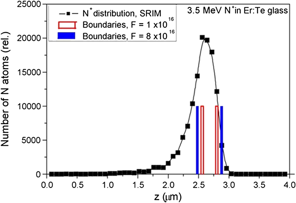 The well (layer 2) is delimited by the sample surface () and the upper (left) boundary of the barrier. Centre of the calculated barrier layer is shifted downwards with respect to the center of the distribution. This may be attributed to the fact that SRIM slightly overestimates stopping power, and consequently predicts lower ranges than the experimental ones. Ion implantation, moreover, may be very effective in introducing a suitable dopant into a glass substrate or a glass WG, with the aim of increasing the functionality of the glass. Particular attention has been directed to the implantation of erbium84,85 or Neodymium86 to achieve the capability of optical amplification. A device fabricated by implanting erbium ions with the concentration of in alumina films was claimed to be then (1996) the world’s smallest erbium-doped optical amplifier.85 The formation of metal nanoparticles in glass by ion implantation has also been attracting the large interest for the fabrication of nonlinear optical devices; a comprehensive review of nonlinear optical properties of implanted metal nanoparticles in various transparent materials was recently published.87 4.3.UV Laser WritingThe fabrication of PICs by all the methods considered so far also requires the use of cleanroom technologies such as lithography and chemical or plasma-based etching, in order to define the channel WGs and the other optical components. Since the lithography and etching approach is costly, cumbersome, and slow for development; in recent years, the search for fast direct writing techniques has been growing up.88 Electron-beam writing is not effective in oxide glasses; chalcogenide glass thin films, however, have been investigated as e-beam resists for nanoscale and ultrathin applications in MEMS/NEMS technology,89 and recent results have proved that ridge optical WGs can be obtained by e-beam writing in chalcogenide films.90 Laser writing, however, exhibits many more advantages and has eventually emerged as a viable rapid-prototyping and small-batch-production technique. Direct UV laser writing is one of the available effective techniques; it exploits the absorption of a specific laser wavelength (generally at around 240 nm) by a photosensitive material to produce a permanent modification of the RI. Despite the disadvantage of requiring photosensitive/photorefractive properties, in practice, this technique can be used on a wide range of materials, obviously including polymers91,92 and crystalline materials such as lithium niobate,93 but also ion exchanged pyrex glasses94 and, more important here, Ge-doped silica glasses. Historically, the way to UV writing in IO was opened by Chandross et al.,95 who used a photochemical reaction produced by a 364 nm laser to fabricate 4-μm wide optical WGs in doped polymer films. As to glassy materials, direct UV writing in a SOS structure was first reported by Svalgaard et al., who demonstrated buried single-mode channel WGs in Ge-doped silica films with a RI increase of .96 Shortly, later the same group and others demonstrated low-loss () WGs 97,98 and components such as directional couplers and power splitters.99 Since then, numerous works have been performed regarding the fabrication of planar lightwave circuits (PLCs), using different photosensitive materials and producing fundamental photonic structures such as optical WGs,100–104 diffractive gratings,105–107 and photonic crystals.108 Although the complete understanding of the microscopic origins of the index variation remains an issue, complementary models have been proposed in order to explain the phenomenon. The three main mechanisms that can be responsible of the modification of the RI can be summarized as follows: (i) color centers, (ii) stress relaxation, and (iii) volume changes; the contribution ratio of each mechanism to the RI change, however, is still under investigation. In the color center model, strong UV absorption due to localized electronic transitions of laser-induced defects gives rise to RI changes in the visible/infrared spectral region according to the Kramers–Kronig relationship.109,110 A typical example is represented by the glass that presents an intense absorption band around 240 nm, originated from Ge related oxygen deficient defects (GODC). The underlying premise of this model is the excitation of localized precursor defects or dopants below the bandgap such as GODC at 240 nm,111 at 250 nm and at 260 nm.112 Moreover, an improvement of the effects can be achieved by loading the material with suitable elements such as boron,113 deuterium,114 and hydrogen.115 A second mechanism is related to the so-called stress relaxation through the photoelastic effect;109 this theory is based on the hypothesis that the RI changes originate from residual stress in materials due to a difference in thermal expansion coefficients between film and substrate. Finally, the last contribution to photosensitivity arises from volume changes such as densification and expansion, which are observed in the form of valley or bumps along the writing path. According to Lorenz–Lorentz relationship,116 compaction increases the RI while the expansion decreases it. The type of volume change depends on the glass structure, which in turn is determined by its composition and the fabrication technique used for its synthesis. For example, typical glasses that show a compaction behavior after irradiation are (i) Ge-doped silicates106 and (ii) gallium–lanthanumsulphides,117 while and Zr–Ba–fluoride glasses exhibit a photoexpansion behavior due to a widening of interlayer distances.118 From a fabrication point of view, the most important parameters of the writing process are: (i) wavelength of the laser, (ii) operation regime, and (iii) composition and geometry of the glass samples. The correct parameters have to be chosen having in mind that focusing high energy into a small volume of material can have detrimental effects if the energy dissipation from the exposed region is not rapid enough. Thermalization of a small volume due to large amounts of energy being coupled into a material with low thermal conductivity may result in local melting and even in vaporization of the material; both these effects are undesirable since they surely lead to an increase of propagation losses, if not to a stop of waveguiding. One direct writing approach uses a cw laser, normally with a wavelength of 244 nm, focused on the photosensitive material; the actual writing occurs translating the structure beneath a tightly focused laser beam by a computer-controlled high-precision translation stage. The typical scanning speeds range from 1 to , resulting in very short exposure times of 0.1 to 400 ms.100,101,119 Another approach makes use of a pulsed laser (usually, a KrF excimer laser source operating at 248 nm) and the definition of the photonic components (WG, grating, etc.) occurs using a single step UV exposure through an amplitude mask. Generally, the mask is constituted by a suitably patterned Ti film, with the thickness of 200 nm, deposited on the photorefractive material. Typical parameters are pulse fluence lower than to prevent damaging of the mask, repetition rate (RR) of 10 Hz, and cumulative exposure dose up to .103,106 Finally, an alternative approach is based on the interference of two UV beams producing a tightly focused writing spot, near circular, that presents micron-order dimension at the intersection point.120 A typical experimental setup is based on cw frequency-doubled Ar-ion laser () with the beam power controlled via an acoustic optical modulator; typical writing values for germanosilicate glasses are: (i) laser power of 100 mW at 244 nm, (ii) translation speed from 10 to , and (iii) fluence of the order of few . Indeed, a significant advantage of the direct writing system with an UV laser is the small spot size of the focused laser beam, which can be used to inscribe both WGs and gratings.121 In the direct grating writing (DGW), rather than using the wide area exposure such as that from a phase mask, the dimensions of the UV induced structure are determined by the focal spot size. A DGW experimental setup is sketched in Fig. 5, together with a photo of the actual system.121 Fig. 5Illustration of (a) direct grating writing (DGW) setup; (b) crossed beams focused on the core layer of the silica-on-silicon substrate; (c) photo of DGW system (Ref. 107). 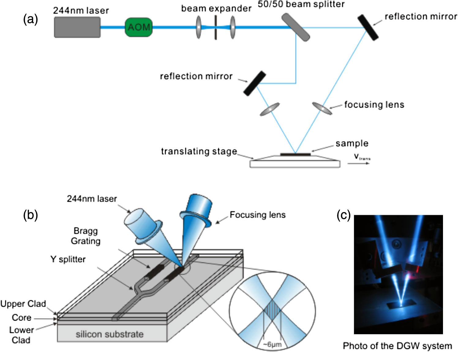 Nowadays, the direct UV writing technique can be considered a consolidated method for the realization of photonic devices; as an example, Stratophase (an UK Company) has recently acquired UV writing technology in order to develop lab-on-chip systems, ranging from individual disposable sensors for biotechnology to multiplexed sensor networks in pharmaceutical manufacturing.122 Even complex integrated optical circuits, useful for the realization of quantum optical states and information networks, have been very recently implemented by UV writing technique.123,124 4.4.Femtosecond-Laser WritingFemtosecond-laser writing (fs-writing) is now one of the most efficient techniques for direct 3-D microfabrication of optical WGs and micromachining of transparent optical materials.125 The seminal paper in this field was published by Hirao, who is demonstrating the possibility to modify the RI of pure and Ge-doped silica glasses as a function of the radiation dose.126 Then, a number of works have been performed concerning not only the fabrication of optical WGs, photonic crystals, diffractive gratings, etc. in various transparent materials, but also micromachining (namely, drilling, etching, and milling). The most important features of fs-writing are the following ones: (i) it is a single-step and mask-less process, so that cost and time consuming are reduced; (ii) it can be applied to different materials (i.e., glasses, crystals, and polymers), just modifying the irradiation parameters (repetition rate, fluence, etc.); (iii) it is an intrinsically 3-D technology because it is possible to induce material variation and to realize optical devices at any arbitrary depth in the substrate. Moreover, by exploiting its micromachining capability, fs-writing makes possible the integration on the same substrate of the IO circuits with microfluidic channels,127,128 as depicted in Fig. 6.129 Fig. 6Illustration of femtosecond-laser direct writing used to add optical WGs to a lab-on-a-chip device designed for capillary electrophoresis. The optical WGs, coupled to optical fibers, excite fluorescence in a highly localized region in the microchannel, and guide emissions to a detector (Ref. 129). 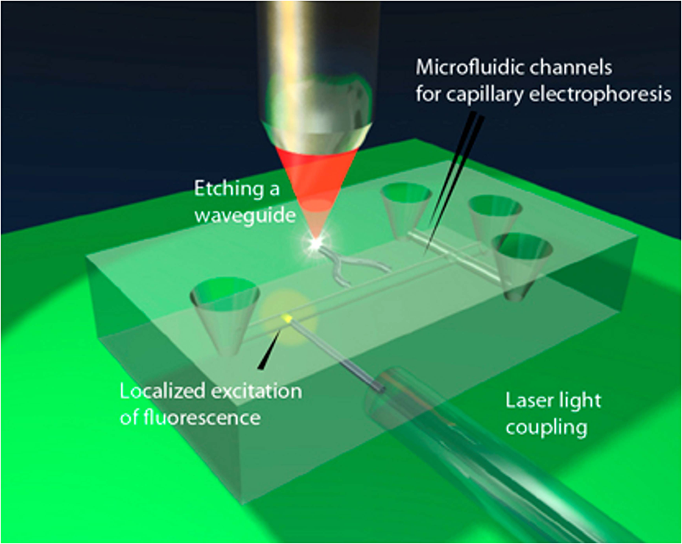 Even in the case of fs-writing, the analysis of the process mechanisms is quite complex and of course also depends on the linear and nonlinear optical properties of the material. The physical origin can concurrently involve several processes, such as ionic rearrangement, lattice stress, heat accumulation, defect creation, changes in local stoichiometry, thermal diffusion, and changes in the electronic polarizability.125,130,131 It is generally agreed, however, that the laser energy is rapidly absorbed through a combination of multiphoton absorption and avalanche photoionization. Mechanisms leading to the formation of WGs and optical components have been investigated in crystalline materials, too.132,133 For low laser intensities, the glass is heated by each pulse and rapidly cools through thermal conduction between pulses. The resulting RI change is determined by the relationship between the density of the glass and the cooling rate, and by the residual stresses caused by this density gradient. For high laser intensities, a plasma forms within the glass, creating a large charge separation that leads to a Coulomb explosion. This results in a shockwave: the pressure induces RI changes with an inhomogeneous redistribution of the material within the modified region, and the stress induces RI changes in the surrounding material. A model that describes the theory of femtosecond laser modification mechanisms is summarized in Fig. 7.130 Fig. 7Illustration of the physical mechanisms of the femtosecond laser writing method. [adapted from Reichman (Ref. 130)].  From a fabrication point of view, the most important parameters that have to be taken into account during the writing step concern writing geometry, pulse energy, and RR. Depending on the direction of translation of the sample under the laser beam, longitudinal or transverse writing can be adopted for the fabrication of optical devices. Longitudinal writing permits to obtain WGs with a cylindrical symmetry; their length, however, is limited by the working distance of the lens which, for a typical focusing objective with , is approximately 5 mm. In the transverse writing scheme, the sample is scanned orthogonally relative to the incoming laser; in this case, the working distance no longer restricts the WGs length and many devices at different depths can be written into the sample, providing 3-D optical circuits. The disadvantage of this approach is that the WG cross section is asymmetric, due to the ratio between depth of focus and spot size. The asymmetry produces elliptical WG cross sections with elliptical guided modes, which cause a poor coupling with external to optical fibers. Suitably shaping the writing laser beam, however, can help to overcome the focal volume’s asymmetry problem; several solutions have been proposed, including astigmatic focusing,134 slit focusing,135 deformable mirror beam reshaping,136 and multiscan writing.137 The laser pulse energy is typically the most influential experimental variable for all the writing configurations. Adjusting the laser fluence by an order of magnitude can cause dramatically different results: from no modification to the controlled modification used for producing optical devices to uncontrolled damage.138 Considering glassy materials, such as fused silica, phosphate glass, and heavy-metal oxide glasses,139 typical energy pulse values for the realization of WGs with low losses are around few μJ in the case of low RR () or of the order of hundreds of nJ in high repetition regime (MHz). For slightly higher pulsed energies, the formation of birefringent nanostructures can be observed, which can lead to photonic devices with polarization dependent characteristic.140 For even higher pulse energies, fs-writing can induce microexplosions, which results in the formation of microvoids; an interesting application for this type of systems can be represented by high density 3-D data storage.141,142 The RR is also a crucial parameter for the realization of optical devices; traditionally, kHz RR amplified fs lasers have been used for fs device fabrication, but the recent development of high power oscillators and other high-RR fs sources has opened up the possibility of writing WGs with . The main differences reported when using high-RR lasers are an increase in the perceived line diameter, and a potentially greater RI modification.143 These features are related to the fact that with high-RR lasers there is insufficient time between pulses for the heat to diffuse out of the focal region, and as a result, heat accumulation occurs.144,145 Additionally, it has been observed that MHz systems provide better quality WGs in some transparent glasses, while kHz systems are preferable for other materials. Currently, it is still unclear why some materials respond better with one laser respect to the other. In a recent study, the thermal stability of femtosecond laser modification inside fused silica has been investigated, and the results have been related to different types of bond rearrangements in the glass network.146 Undoubtedly, fs-laser writing technique permits to obtain low-loss WGs in different types of glasses, as proved by a number of reports: Nasu et al.137 have demonstrated that it is possible, using a multiscan writing scheme, to induce in fused silica a RI change of , suitable for WGs with propagation loss of at 1550 nm and for low loss coupling to single-mode fibers; in phosphate glasses, using a scan of with a 1 kHz, 150-fs Ti:Sapphire laser with 0.3 NA microscope objective, and 5 μJ pulse energy, devices were produced with damping loss of about at 1550 nm;134 in heavy metal oxide, using a 1 kHz, 100-fs Ti:Sapphire laser with 0.42 NA objective, and 1.8 μJ pulse energy, WGs with loss below at 633 nm were realized.139 It is also worth pointing out that fs-laser micromachining has been successfully applied in a number of more exotic glasses, such as tellurite glasses,147 where other fabrication techniques do not easily apply; oxyfluoride silicate systems,148 that are considered a promising host for RE because they combine the attractive spectroscopic properties of the fluoride glass with the structural compatibility and stability of silica; Bi-doped silica glasses,149 which exhibit broadband emission around 1.3 μm; high quantum efficiency Er-doped Baccarat glasses;150 phospho-tellurite glasses,151 that can exhibit ultra-broadband amplification in S-C-L telecom bands (1460 to 1625 nm); Er–Yb-doped tellurium zinc glasses;152 Tm:ZBLAN glass,153 where in a 9-mm long planar chip, an 1.89 μm free-running cw laser has been fabricated, which produces 205 mW and achieves a 67% internal slope efficiency, corresponding to a quantum efficiency of 161%. With reference to this last result, as a proof of the enormous advance in technology in the last 12 years, let us just recall that in the first active device obtained by fs-laser writing in a commercial Nd-doped () silica glass rod a signal enhancement of 1.5 dB/cm at 1054 nm was achieved with an incident pump power of 350 mW.154 Finally, the direct-write approach has proved to be suitable for the rapid development of sophisticated quantum optical circuits and their scaling into 3-D.155,156 5.Conclusions and PerspectivesThe advance of modern technology is still largely driven by miniaturization, and PICs are expected to play an even more important role in optical communications, imaging, computing, and sensing. Recent developments in materials and technologies have expanded the number of optical functions to be implemented in a single integrated optical chip. Two major platforms for PICs are constituted by SOI hybrid technology and InP monolithic technology. SOI WG structures are defined on a Si wafer (e.g., 200 mm or 8 in.) in a CMOS pilot line. A typical SOI wafer consists of a 220 nm Si core layer on top of a 2 μm buried cladding layer fabricated on the silicon wafer. Direct band gap III–V layer (InP/InGaAsP) heterostructures can then be integrated on top of the SOI WG substrate; one approach makes use of a polymer bonding layer to bond III–V dies onto the SOI, so that, after removal of the original InP growth substrate, only a thin epitaxial InP/InGaAsP film remains attached to the SOI WG circuit: laser diodes and photodetectors can finally be fabricated in it on a wafer scale and lithographically aligned to the underlying SOI WG circuit.157 An alternative approach, followed among others by Infinera,158 uses a single material—indium phosphide (InP)—with which it is possible to fabricate all the necessary optical functions on a single semiconductor chip. Infinera’s DTN-X platform supports superchannels based on next generation coherent PICs, which integrate over 600 optical functions into just two optical chips, one for transmit and one for receive. Despite these challenging competitors, glass remains one of the most important materials even in the era of photonics; perspectives of a large functional integration based on SOS and novel glass platforms are becoming quite real, due to the advanced development of fabrication technologies of glass WGs. One should not forget some pioneering works in this area, especially by groups at AT&T Bell Labs and at NTT Photonics Laboratories, such as the fabrication by Adar et al.159 of strong Bragg reflectors, nearly polarization independent, embedded into fiber-matched silica-on-silicon WGs; or the development of optical switches and WDM modules at NTT using silica-based PLC technology since the 1980s.160,161 Ion exchange in glass, PECVD, and FHD are mature technologies, which have already led to the production of high-quality, low-loss, low-cost passive components for optical communication systems and optical interconnections. It is worth recalling that record low losses below have been achieved in different glass systems and by different processes: for instance, Adar et al. reported single-mode propagation loss of in phosphorus-doped cores deposited through plasma-enhanced CVD,162 while Kominato et al., using a larger, multimode core design, reported propagation loss for germanium-doped cores deposited by flame hydrolysis.163 Integrated optical devices made by other processes, like sol–gel deposition, ion implantation, and fs-laser writing, are perhaps still not fully ready for the market, but these technologies keep having a great potential: in its many variations, the sol–gel process offers a viable route to the preparation of virtually every kind of glasses and composites, in any desired shape, while ion implantation and fs-laser writing permit to define even 3-D guided structures in a large variety of materials, amorphous, and crystalline. Femtosecond laser written WGs exhibit low losses, and photonic lattices with one or two transverse dimensions fabricated by this technique in fused silica have emerged as a versatile system for the experimental investigation of light propagation in discrete optical systems with Kerr nonlinearity, with possible application in photonic circuitry based on switching with blocker solitons.164 Among the emerging deposition technologies in photonics one should also include atomic layer deposition (ALD), which is a CVD-type process based on sequential, self-limiting surface reactions and typically performed at low temperature, capable of thickness control at the Ångstrom or monolayer level.165 ALD films remain extremely smooth, pinhole-free, and conformal to the original substrate: all qualities that are extremely important in the case of waveguiding dielectric films and integrated optical components. As a matter of fact, the basic technology dates back to 1974, with the pioneering work of Suntola.166 Atomic Layer Evaporation (ALE—as it was named in that first paper) epitaxy soon became the elective method of depositing thin semiconducting films on a substrate for thin film electroluminescent devices’ production. The term ALE switched to ALD in the 2000s, due to the fact that amorphous dielectric films were becoming more and more important and that therefore epitaxy was no more a peculiarity. The excellent characteristics of ALD films have recently increased the interest toward photonic applications, with the demonstration, among others, of low-loss WGs167 and of amorphous and crystallization-controlled WGs.168,169 Moreover, the ability to conformally coat nanostructured surface results in unique possibilities,170 and the development of ALD processes for novel materials has a strong potential for significant breakthroughs in the fabrication of monolithically integrated devices. Nanostructured and nanocomposite glasses (e.g., GCs) are also assuming larger importance, due to the enhancement of their optical, spectroscopic, and thermal properties with respect to the corresponding amorphous matrices. New horizons have also been opened by the development of another versatile platform, based on chalcogenide glasses, which exhibit high RI, high mid-IR ( to 20 μm) transmittance, and high nonlinearity. Chalcogenide glasses can be formed with a variety of compositions and doped with additional elements to provide further functionality (e.g., with rare-earth elements). 3-D photonic circuits can be written by femtosecond laser.171 Hybrid integration of chalcogenide glass WGs and quantum cascade lasers has also been demonstrated.172 Demonstrated or envisioned applications include light amplification and generation,173–175 all-optical signal processing,176 spectroscopic chemical sensing,177,178 astrophotonics, and biochemical sensing.170,179 Finally, the quest for high-performance platforms for integrated nonlinear optics has led to two new material structures, which also offer CMOS compatibility and have already achieved considerable success, based on silicon nitride () and high-index doped silica, trade named Hydex.180 An integrated silicon and ultra-low-loss WG platform has also been demonstrated, with minimum propagation loss measured in the silicon nitride core equal to in the 1590-nm wavelength regime.181 As to Hydex™, it was developed as a high- system for low-loss WGs;182 it is a robust material that is deposited through conventional CVD processes, with RI contrast adjustable from 0% to over 20%, and propagation losses estimated to be as small as .183 Using the dispersion characteristics of this glass, supercontinuum (SC) generation was achieved in a 45-cm long spiral WG, obtaining an SC spectral width of at both 1290 and 1550 nm.184 We can therefore conclude that the prospects of integrated optical devices in glass are still very good, with continuously growing applications in the area of on-chip devices and biosensors. Optimization of the synthesis processes of glasses tailored for the specific application and of the WG fabrication technologies may guarantee that new record performances of glass PICs will be achieved. AcknowledgmentsThe authors are grateful to Maurizio Ferrari for his valuable comments and to Alessandro Carpentiero for his technical assistance and figure drawing; both are at IFN-CNR in Trento. ReferencesS. E. Miller,
“Integrated optics: an introduction,”
Bell Syst. Tech. J., 48
(1), 20592069
(1969). http://dx.doi.org/10.1002/bltj.1969.48.issue-7 BSTJAN 0005-8580 Google Scholar
I. P. Kaminow,
“Optical integrated circuits: a personal perspective,”
J. Lightwave Technol., 26
(9), 994
–1004
(2008). http://dx.doi.org/10.1109/JLT.2008.922149 JLTEDG 0733-8724 Google Scholar
P. S. Patil,
“Versatility of chemical spray pyrolysis technique,”
Mater. Chem. Phys., 59
(3), 185
–198
(1999). http://dx.doi.org/10.1016/S0254-0584(99)00049-8 MCHPDR 0254-0584 Google Scholar
R. Martinez-Martinezet al.,
“Blue-yellow photoluminescence from energy transfer in films deposited by ultrasonic spray pyrolysis,”
J. Alloys Compd., 509
(6), 3160
–3165
(2011). http://dx.doi.org/10.1016/j.jallcom.2010.11.203 JALCEU 0925-8388 Google Scholar
C. N. Afonsoet al.,
“Pulsed laser deposition for functional optical films,”
Laser Ablation and its Applications, 315
–338 Springer, New York
(2007). Google Scholar
C. N. Afonsoet al.,
“Rare-earth doped glass waveguides prepared by pulsed laser deposition,”
Appl. Surf. Sci., 96–98 760763
(1996). http://dx.doi.org/10.1016/0169-4332(95)00550-1 ASUSEE 0169-4332 Google Scholar
M. Martinoet al.,
“Pulsed laser deposition of active waveguides,”
Thin Solid Films, 433
(1–2), 39
–44
(2003). http://dx.doi.org/10.1016/S0040-6090(03)00310-9 THSFAP 0040-6090 Google Scholar
M. Irannejadet al.,
“Active glass waveguide amplifier on GaAs by UV-pulsed laser deposition and femtosecond laser inscription,”
Laser Phys. Lett., 9
(5), 329
–339
(2012). http://dx.doi.org/10.7452/lapl.201110101 1612-2011 Google Scholar
J. E. GoellR. D. Standley,
“Sputtered glass waveguide for integrated optical circuits,”
Bell Syst. Tech. J., 48
(10), 3445
–3448
(1969). http://dx.doi.org/10.1002/bltj.1969.48.issue-10 BSTJAN 0005-8580 Google Scholar
Physical Vapor Deposition, Airco Temscal, Berkeley
(1986). Google Scholar
J. C. G. de Sandeet al.,
“Optical properties of sputtered, laser and e-beam deposited a-Ge films: an ellipsometric study,”
Appl. Opt., 31
(28), 6133
–6138
(1992). http://dx.doi.org/10.1364/AO.31.006133 APOPAI 0003-6935 Google Scholar
Thin Films Materials Technology: Sputtering of Compound Materials, Springer, New York
(2012). Google Scholar
C. W. Pitt,
“Materials and fabrication techniques for integrated optics: organic and amorphous materials,”
J. Non-Cryst. Solids, 47
(2), 159
–174
(1982). http://dx.doi.org/10.1016/0022-3093(82)90058-8 JNCSBJ 0022-3093 Google Scholar
R. RabadyI. Avrutsky,
“Titania silicon dioxide, and tantalum pentoxide waveguides and optical resonant filters prepared with radio-frequency magnetron sputtering and annealing,”
Appl. Opt., 44
(3), 378
–383
(2005). http://dx.doi.org/10.1364/AO.44.000378 APOPAI 0003-6935 Google Scholar
A. Chiaseraet al.,
“-activated silica–titania planar waveguides for EDPWAs fabricated by RF-sputtering,”
J. Non-Cryst. Solids, 322
(1–3), 289
–294
(2003). http://dx.doi.org/10.1016/S0022-3093(03)00217-5 JNCSBJ 0022-3093 Google Scholar
A. Chiaseraet al.,
“High quality factor -activated dielectric microcavity fabricated by RF sputtering,”
Appl. Phys. Lett., 89
(17), 171910
(2006). http://dx.doi.org/10.1063/1.2364841 APPLAB 0003-6951 Google Scholar
J. A. Frantzet al.,
“Waveguide amplifiers in sputtered films of -doped gallium lanthanum sulfide glass,”
Opt. Express, 14
(5), 1797
–1803
(2006). http://dx.doi.org/10.1364/OE.14.001797 OPEXFF 1094-4087 Google Scholar
M. L. Anneet al.,
“Chalcogenide glass optical waveguides for infrared biosensing,”
Sensors, 9
(9), 7398
–7411
(2009). http://dx.doi.org/10.3390/s90907398 SNSRES 0746-9462 Google Scholar
Handbook of Chemical Vapor Deposition, 2nd ed.William Andrew Publishing, Norwich, NY
(1999). Google Scholar
Principles of Chemical Vapor Deposition, Kluwer Academic, Dordrecht
(2003). Google Scholar
M. KawachiM. YasuT. Edahiro,
“Fabrication of glass planar optical waveguides by flame hydrolysis deposition,”
Electron. Lett., 19
(15), 583
–584
(1983). http://dx.doi.org/10.1049/el:19830398 ELLEAK 0013-5194 Google Scholar
J. P. BangeL. S. PatilD. K. Gautam,
“Growth and characterization of films deposited by flame hydrolysis deposition,”
Prog. Electromagn. Res. M, 3 165
–175
(2008). http://dx.doi.org/10.2528/PIERM08060401 1937-8726 Google Scholar
A. TurtsevichO. NalivaikoL. Anufriev,
“LPCVD borophosphosilicate-glass films: deposition and properties,”
Russ. Microelectr., 36
(4), 251
–260
(2007). http://dx.doi.org/10.1134/S1063739707040051 RUICE5 1063-7397 Google Scholar
Plasma-Enhanced Chemical Vapor Deposition, ,1997). Google Scholar
Simulation of Deposition Processes with PECVD Apparatus: Theory and Applications, Nova Science Publishers Inc., Hauppauge, New York
(2012). Google Scholar
X. LinX. MaJ. J. He,
“Void-filling and loss reduction in PECVD silica waveguide devices using boron–germanium codoped upper cladding,”
IEEE Photonic Technol. Lett., 22
(20), 1491
–1493
(2010). http://dx.doi.org/10.1109/LPT.2010.2064292 IPTLEL 1041-1135 Google Scholar
T. Saitoet al.,
“Photosensitivity in silica-based waveguides deposited by atmospheric pressure chemical vapor deposition,”
Appl. Opt., 37
(12), 2242
–2244
(1998). http://dx.doi.org/10.1364/AO.37.002242 APOPAI 0003-6935 Google Scholar
V. HopfeD. W. Sheel,
“Atmospheric-pressure pecvd coating and plasma chemical etching for continuous processing,”
IEEE Trans. Plasma Sci., 35
(2), 204
–214
(2007). http://dx.doi.org/10.1109/TPS.2007.893248 ITPSBD 0093-3813 Google Scholar
J. M. Ruanoet al.,
“Flame hydrolysis deposition of glass on silicon for the integration of optical and microfluidic devices,”
Anal. Chem., 72
(5), 1093
–1097
(2000). http://dx.doi.org/10.1021/ac9906983 ANCHAM 0003-2700 Google Scholar
F. AyA. AydinliaS. Agan,
“Low-loss as-grown germanosilicate layers for optical waveguides,”
Appl. Phys. Lett., 83
(23), 4743
–4745
(2003). http://dx.doi.org/10.1063/1.1631753 APPLAB 0003-6951 Google Scholar
X. LinX. MaJ.-J. He,
“Void-filling and loss reduction in PECVD silica waveguide devices using boron–germanium codoped upper cladding,”
IEEE Photonic Technol. Lett., 22
(20), 1491
–1493
(2010). http://dx.doi.org/10.1109/LPT.2010.2064292 IPTLEL 1041-1135 Google Scholar
Sol–Gel Optics: Processing and Applications, Kluwer Academic Publishers, Dordrecht, the Netherlands
(1994). Google Scholar
M. Ebelmen,
“Recherches sur les combinaisons des acides borique et silicique avec les ethers,”
Ann. Chim. Phys., 16 129
–166
(1846). ACPHAA 0365-1444 Google Scholar
L. L. HenchJ. K. West,
“The sol–gel process,”
Chem. Rev., 90
(1), 33
–72
(1990). http://dx.doi.org/10.1021/cr00099a003 CHREAY 0009-2665 Google Scholar
Y. Jestinet al.,
“Low-loss optical -activated glass-ceramics planar waveguides fabricated by bottom-up approach,”
Appl. Phys. Lett., 91
(7), 071909
(2007). http://dx.doi.org/10.1063/1.2771537 APPLAB 0003-6951 Google Scholar
A. Peledet al.,
“Monolithic rare-earth doped sol–gel tapered rib waveguide laser,”
App. Phys. Lett., 92
(22), 221104
(2008). http://dx.doi.org/10.1063/1.2936961 APPLAB 0003-6951 Google Scholar
P. K. Biswas,
“Sol–gel thin films for optics and photonics,”
J. Sol–Gel Sci. Technol., 59
(3), 456
–474
(2011). http://dx.doi.org/10.1007/s10971-010-2368-5 JSGTEC 0928-0707 Google Scholar
N. ChiodiniA. PaleariM. Romagnoli,
“Nanostructured glass ceramic: a competitor for Si nanodots in silica,”
Proc. SPIE, 5925 59250J
(2005). http://dx.doi.org/10.1117/12.616537 PSISDG 0277-786X Google Scholar
L. Zampedriet al.,
“Erbium-activated silica–titania planar waveguides,”
J. Sol–Gel Sci. Technol., 26
(1–3), 1033
–1036
(2003). http://dx.doi.org/10.1023/A:1020734018629 JSGTEC 0928-0707 Google Scholar
R. R. Gonçalveset al.,
“Erbium-activated silica–zirconia planar waveguides prepared by sol–gel route,”
Thin Solid Films, 516
(10), 3094
–3097
(2008). http://dx.doi.org/10.1016/j.tsf.2007.07.183 THSFAP 0040-6090 Google Scholar
R. R. Gonçalveset al.,
“Sol–gel Er-doped planar waveguides: a viable system for 1.5 mm application,”
App. Phys. Lett., 81
(1), 28
–30
(2002). http://dx.doi.org/10.1063/1.1489477 APPLAB 0003-6951 Google Scholar
L. Minatiet al.,
“X-ray photoelectron spectroscopy of erbium-activated silica–hafnia waveguides,”
J. Non-Cryst. Solids, 353
(5), 502
–505
(2007). http://dx.doi.org/10.1016/j.jnoncrysol.2006.10.018 JNCSBJ 0022-3093 Google Scholar
A. Chiappiniet al.,
“Sol–gel-derived photonic structures: fabrication, assessment, and application,”
J. Sol–Gel Sci. Technol., 60
(3), 408
–425
(2011). http://dx.doi.org/10.1007/s10971-011-2556-y JSGTEC 0928-0707 Google Scholar
P. Moriarty,
“Nanostructured materials,”
Rep. Prog. Phys., 64 297
–381
(2001). http://dx.doi.org/10.1088/0034-4885/64/3/201 RPPHAG 0034-4885 Google Scholar
P. HartmannR. JedamzikT. Westerhoff,
“Zero-expansion glass ceramic ZERODUR: recent developments reveal high potential,”
Proc. SPIE, 8450 845022
(2012). http://dx.doi.org/10.1117/12.926047 PSISDG 0277-786X Google Scholar
Y. WangJ. Ohwaki,
“New transparent vitroceramics codoped with and for efficient frequency upconversion,”
Appl. Phys. Lett., 63
(24), 3268
–3270
(1993). http://dx.doi.org/10.1063/1.110170 APPLAB 0003-6951 Google Scholar
P. A. Tick,
“Are low-loss glass ceramic optical waveguides possible?,”
Opt. Lett., 23
(24), 1904
–1905
(1998). http://dx.doi.org/10.1364/OL.23.001904 OPLEDP 0146-9592 Google Scholar
C. Goyeset al.,
“ laser annealing on erbium-activated glass–ceramic waveguides for photonics,”
Opt. Mater., 31
(9), 1310
–1314
(2009). http://dx.doi.org/10.1016/j.optmat.2008.10.005 OMATET 0925-3467 Google Scholar
P. A. TickN. F. BorrelliI. M. Reaney,
“The relationship between structure and transparency in glass-ceramic materials,”
Opt. Mater., 15
(1), 81
–91
(2000). http://dx.doi.org/10.1016/S0925-3467(00)00017-3 OMATET 0925-3467 Google Scholar
Y. Jestinet al.,
“Erbium activated based glass–ceramics waveguides for photonics,”
J. Non-Cryst. Solids, 353
(5–7), 494
–497
(2007). http://dx.doi.org/10.1016/j.jnoncrysol.2006.10.016 JNCSBJ 0022-3093 Google Scholar
I. Alekseevaet al.,
“Optical applications of glass-ceramics,”
J. Non-Cryst. Solids, 356
(52–54), 3042
–3058
(2010). http://dx.doi.org/10.1016/j.jnoncrysol.2010.05.103 JNCSBJ 0022-3093 Google Scholar
Y. Tenget al.,
“Glass-ceramics for photonic devices,”
J. Ceram. Soc. Jpn., 120
(1407), 458
–466
(2012). http://dx.doi.org/10.2109/jcersj2.120.458 JCSJEW 0914-5400 Google Scholar
A. A. Lipovskiiet al.,
“Optical waveguides in electrooptical nanophase glass-ceramics,”
Mater. Lett., 58
(7–8), 1231
–1233
(2004). http://dx.doi.org/10.1016/j.matlet.2003.09.043 MLETDJ 0167-577X Google Scholar
S. N. B. Bhakthaet al.,
“Enhanced fluorescence from in low-loss silica glass-ceramic waveguides with high content,”
App. Phys. Lett., 93
(21), 211904
(2008). http://dx.doi.org/10.1063/1.3037224 APPLAB 0003-6951 Google Scholar
G. Alombert-Gogetet al.,
“ co-activated silica–hafnia glass ceramic waveguides,”
Opt. Mater., 33
(2), 227
–230
(2010). http://dx.doi.org/10.1016/j.optmat.2010.09.030 OMATET 0925-3467 Google Scholar
T. T. Van Tranet al.,
“Erbium-activated silica–tin oxide glass ceramics for photonic integrated circuits: fabrication, characterisation, and assessment,”
Proc. SPIE, 8431 84311F
(2012). http://dx.doi.org/10.1117/12.922595 PSISDG 0277-786X Google Scholar
S. Berneschiet al.,
“Rare earth-activated glass-ceramic in planar format,”
Opt. Eng., 50
(7), 071105
(2011). http://dx.doi.org/10.1117/1.3559211 OPEGAR 0091-3286 Google Scholar
P. Mazzoldiet al.,
“Ion exchange process: history, evolution and applications,”
Riv. Nuovo Cimento, 36
(9), 397
–460
(2013). http://dx.doi.org/10.1393/ncr/i2013-10092-1 RNUCAC 0035-5917 Google Scholar
T. IzawaH. Nakagome,
“Optical waveguide formed by electrically induced migration of ions in glass plates,”
Appl. Phys. Lett., 21
(12), 584
–586
(1972). http://dx.doi.org/10.1063/1.1654265 APPLAB 0003-6951 Google Scholar
T. G. Giallorenziet al.,
“Optical waveguides formed by thermal migrations of ions in glass,”
Appl. Opt., 12
(6), 1240
–1245
(1973). http://dx.doi.org/10.1364/AO.12.001240 APOPAI 0003-6935 Google Scholar
R. V. RamaswamyR. Srivastava,
“Ion-exchanged glass waveguides: a review,”
IEEE J. Light. Technol., 6
(6), 984
–1001
(1988). http://dx.doi.org/10.1109/50.4090 JLTEDG 0733-8724 Google Scholar
G. C. RighiniS. Pelli,
“Ion exchange in glass: a mature technology for photonic devices,”
Proc. SPIE, 4453 93
–99
(2001). http://dx.doi.org/10.1117/12.447638 PSISDG 0277-786X Google Scholar
A. TervonenB. R. WestS. Honkanen,
“Ion-exchanged glass waveguide technology: a review,”
Opt. Eng., 50
(7), 071107
(2011). http://dx.doi.org/10.1117/1.3559213 OPEGAR 0091-3286 Google Scholar
S. Pelliet al.,
“Testing of optical waveguides (TOW) cooperative project: preliminary results of the characterization of k-exchanged waveguides,”
Proc. SPIE, 2212 126
–131
(1994). http://dx.doi.org/10.1117/12.185102 PSISDG 0277-786X Google Scholar
G. Liet al.,
“Systematic modeling study of channel waveguide fabrication by thermal silver ion exchange,”
Appl. Opt., 45
(8), 1743
–1755
(2006). http://dx.doi.org/10.1364/AO.45.001743 APOPAI 0003-6935 Google Scholar
J. AlbertJ. W. J. Lit,
“Full modeling of field-assisted ion-exchange for graded-index buried channel optical waveguides,”
Appl. Opt., 29
(18), 2798
–2804
(1990). http://dx.doi.org/10.1364/AO.29.002798 APOPAI 0003-6935 Google Scholar
J. Linareset al.,
“Buried waveguides fabricated by a purely thermal ion back diffusion in glass and assisted by electric field: a new model,”
Proc. SPIE, 2212 138
–145
(1994). http://dx.doi.org/10.1117/12.185104 PSISDG 0277-786X Google Scholar
J. GrelinE. GhibaudoJ.-E. Broquin,
“Study of deeply buried waveguides: a way towards 3D integration,”
Mater. Sci. Eng. B, 149
(2), 185
–189
(2008). http://dx.doi.org/10.1016/j.mseb.2007.11.013 MSBTEK 0921-5107 Google Scholar
N. A. SanfordK. J. MaloneD. R. Larson,
“Integrated-optic laser fabricated by field-assisted ion exchange in neodymium-doped soda-lime-silicate glass,”
Opt. Lett., 15
(7), 366
–368
(1990). http://dx.doi.org/10.1364/OL.15.000366 OPLEDP 0146-9592 Google Scholar
B. BucholdE. Voges,
“Polarisation insensitive arrayed waveguide grating multiplexers with ion-exchanged waveguides in glass,”
Electron. Lett., 32
(24), 2248
–2250
(1996). http://dx.doi.org/10.1049/el:19961493 ELLEAK 0013-5194 Google Scholar
P. Camyet al.,
“Ion-exchanged planar lossless splitter at 1.5 μm,”
Electron. Lett., 32
(4), 321
–323
(1996). http://dx.doi.org/10.1049/el:19960267 ELLEAK 0013-5194 Google Scholar
D. Barbieret al.,
“Amplifying four-wavelength combiner, based on erbium/ytterbium-doped waveguide amplifiers and integrated splitters,”
IEEE Photonic. Technol. Lett., 9
(3), 315
–317
(1997). http://dx.doi.org/10.1109/68.556058 IPTLEL 1041-1135 Google Scholar
D. F. Geraghtyet al.,
“Ion-exchanged waveguide add/drop filter,”
Electron. Lett., 37
(13), 829
–831
(2001). http://dx.doi.org/10.1049/el:20010572 ELLEAK 0013-5194 Google Scholar
D. L. Veaseyet al.,
“Arrays of distributed-Bragg-reflector waveguide lasers at 1536 nm in Yb/Er codoped phosphate glass,”
Appl. Phys. Lett., 74
(6), 789
–791
(1999). http://dx.doi.org/10.1063/1.123368 APPLAB 0003-6951 Google Scholar
P. Madasamyet al.,
“Waveguide distributed Bragg reflector laser arrays in erbium doped glass made by dry Ag film ion exchange,”
Opt. Eng., 41
(5), 1084
–1086
(2002). http://dx.doi.org/10.1117/1.1466852 OPEGAR 0091-3286 Google Scholar
S. Blaizeet al.,
“Multiwavelengths DFB waveguide laser arrays in Yb-Er codoped phosphate glass substrate,”
IEEE Photonic. Technol. Lett., 15
(4), 516
–518
(2003). http://dx.doi.org/10.1109/LPT.2003.809306 IPTLEL 1041-1135 Google Scholar
Optical Effects of Ion Implantation, Cambridge University, Cambridge
(1994). Google Scholar
Ion Implantation and Synthesis of Materials, Springer-Verlag, Berlin
(2006). Google Scholar
SRIM-The Stopping and Range of Ions in Matter, Lulu Press, Morrisville, USA
(2012). http://www.srim.org Google Scholar
S. Pelliet al.,
“Confocal luminescence microscopy characterization of optical waveguides produced by ion beam irradiation on LiF,”
Proc. SPIE, 4987 13
–20
(2003). http://dx.doi.org/10.1117/12.478329 PSISDG 0277-786X Google Scholar
F. ChenX.-L. WangK.-M. Wang,
“Development of ion-implanted optical waveguides in optical materials: a review,”
Opt. Mater., 29
(11), 1523
–1542
(2007). http://dx.doi.org/10.1016/j.optmat.2006.08.001 OMATET 0925-3467 Google Scholar
S. Berneschiet al.,
“Ion beam irradiated channel waveguides in -doped tellurite glass,”
Appl. Phys. Lett., 90
(12), 121136
(2007). http://dx.doi.org/10.1063/1.2717085 APPLAB 0003-6951 Google Scholar
I. Bányászet al.,
“M-line spectroscopic, spectroscopic ellipsometric and microscopic measurements of optical waveguides fabricated by MeV-energy ion irradiation for telecom applications,”
Thin Solid Films, 541 3
–8
(2013). http://dx.doi.org/10.1016/j.tsf.2012.11.134 THSFAP 0040-6090 Google Scholar
E. R. SchinellerR. P. FlamD. W. Wilmot,
“Optical waveguides formed by proton irradiation of fused silica,”
J. Opt. Soc. Am., 58
(9), 1171
–1176
(1968). http://dx.doi.org/10.1364/JOSA.58.001171 JOSAAH 0030-3941 Google Scholar
R. G. StandleyW. M. GibsonJ. W. Rodgers,
“Properties of ion-bombarded fused quartz for integrated optics,”
Appl. Opt., 11
(6), 1313
–1316
(1972). http://dx.doi.org/10.1364/AO.11.001313 APOPAI 0003-6935 Google Scholar
A. Polman et al.,
“1.54 μm room temperature luminescence of MeV erbium implanted silica glass,”
Appl. Phys. Lett., 57
(26), 2859
–2861
(1990). http://dx.doi.org/10.1063/1.104203 APPLAB 0003-6951 Google Scholar
G. N. van den Hovenet al.,
“Net optical gain at 1.53 μm in Er-doped waveguides on silicon,”
Appl. Phys. Lett., 68
(14), 1886
–1888
(1996). http://dx.doi.org/10.1063/1.116283 APPLAB 0003-6951 Google Scholar
C. Meneghiniet al.,
“Luminescence from neodymium-ion-implanted waveguides,”
J. Opt. Soc. Am. B, 15
(4), 1305
–1308
(1998). http://dx.doi.org/10.1364/JOSAB.15.001305 JOBPDE 0740-3224 Google Scholar
A. L. Stepanov,
“Nonlinear optical properties of implanted metal nanoparticles in various transparent matrixes: a review,”
Rev. Adv. Mater. Sci., 27
(2), 115
–145
(2011). 1605-8127 Google Scholar
G. C. Righiniet al.,
“Laser irradiation, ion implantation, and e-beam writing of integrated optical structures,”
Proc. SPIE, 5840 649
(2005). http://dx.doi.org/10.1117/12.609231 PSISDG 0277-786X Google Scholar
A. Kovalskiyet al.,
“Chalcogenide glass e-beam and photoresists for ultrathin grayscale patterning,”
J. Micro/Nanolithogr., MEMS, MOEMS, 8
(4), 043012
(2009). http://dx.doi.org/10.1117/1.3273966 JMMMHG 1932-5150 Google Scholar
G. B. HoffmanR. M. Reano,
“Electron beam direct write of chalcogenide glass integrated optics,”
J. Vac. Sci. Technol. B, 30
(6), 06F301
(2012). http://dx.doi.org/10.1116/1.4748567 JVTBD9 0734-211X Google Scholar
J. S. Kooet al.,
“UV written waveguide devices using crosslinkable PMMA-based copolymers,”
Electron. Lett., 39
(4), 394
–395
(2003). http://dx.doi.org/10.1049/el:20030274 ELLEAK 0013-5194 Google Scholar
X. Feiet al.,
“Synthesis of UV-writing fluorinated polymer for organic optical waveguide,”
Adv. Mater. Res., 690–693 1604
–1608
(2013). http://dx.doi.org/10.4028/www.scientific.net/AMR.690-693 ADMRBX 0568-0018 Google Scholar
K. Galloet al.,
“Ultraviolet writing of channel waveguides in proton-exchanged ,”
J. Appl. Phys., 101
(1), 014110
(2007). http://dx.doi.org/10.1063/1.2400511 JAPIAU 0021-8979 Google Scholar
A. K. Sheridanet al.,
“Channel waveguides in ion-exchanged pyrex by direct UV writing,”
Opt. Commun., 242
(1–3), 109
–114
(2004). http://dx.doi.org/10.1016/j.optcom.2004.08.014 OPCOB8 0030-4018 Google Scholar
E. A. Chandrosset al.,
“Photolocking—a new technique for fabricating optical waveguide circuits,”
Appl. Phys. Lett., 24
(2), 72
–74
(1974). http://dx.doi.org/10.1063/1.1655099 APPLAB 0003-6951 Google Scholar
M. Svalgaardet al.,
“Direct UV writing of buried singlemode channel waveguides in Ge-doped silica films,”
Electron. Lett., 30
(17), 1401
–1403
(1994). http://dx.doi.org/10.1049/el:19940935 ELLEAK 0013-5194 Google Scholar
M. SvalgaardM. Kristensen,
“Directly UV written silica-on-silicon planar waveguides with low loss,”
Electron. Lett., 33
(10), 861
–863
(1997). http://dx.doi.org/10.1049/el:19970602 ELLEAK 0013-5194 Google Scholar
D. Zauneret al.,
“Directly UV written silica-on-silicon planar waveguides with low insertion loss,”
Electron. Lett., 34
(16), 1582
–1584
(1998). http://dx.doi.org/10.1049/el:19981091 ELLEAK 0013-5194 Google Scholar
M. Svalgaard,
“Direct writing of planar waveguide power splitters and directional couplers using a focused ultraviolet laser beam,”
Electron. Lett., 33
(20), 1694
–1695
(1997). http://dx.doi.org/10.1049/el:19971138 ELLEAK 0013-5194 Google Scholar
D. Milaneseet al.,
“Photosensitivity and directly UV written waveguides in an ion exchangeable bulk oxide glass,”
Opt. Mater., 18
(3), 295
–300
(2001). http://dx.doi.org/10.1016/S0925-3467(01)00117-3 OMATET 0925-3467 Google Scholar
C. ContardiE. R. TaylorA. Fu,
“Study of UV-written channels in lead silicate glasses,”
J. Non-Cryst. Solids, 291
(1–2), 113
–120
(2001). http://dx.doi.org/10.1016/S0022-3093(01)00796-7 JNCSBJ 0022-3093 Google Scholar
H. Ebendorff-Heidepriem,
“Laser writing of waveguides in photosensitive glasses,”
Opt. Mater., 25
(2), 109
–115
(2004). http://dx.doi.org/10.1016/S0925-3467(03)00258-1 OMATET 0925-3467 Google Scholar
G. Nunzi Contiet al.,
“UV photoimprinting of channel waveguides on active sputtered thin films,”
Appl. Phys. Lett., 89
(12), 121102
(2006). http://dx.doi.org/10.1063/1.2355472 APPLAB 0003-6951 Google Scholar
S. Berneschiet al.,
“Highly photorefractive activated sol–gel thin film waveguides,”
Proc. SPIE, 7604 760402
(2010). http://dx.doi.org/10.1117/12.843210 PSISDG 0277-786X Google Scholar
G. D. Emmersonet al.,
“All-UV-written integrated planar Bragg gratings and channel waveguides through single-step direct grating writing,”
IEE Proc. Optoelectron., 151
(2), 119
–122
(2004). http://dx.doi.org/10.1049/ip-opt:20040182 IPOPE8 1350-2433 Google Scholar
S. Sebastianiet al.,
“Characterization of a highly photorefractive RF-sputtered waveguide,”
Opt. Express, 13
(5), 1696
–1701
(2005). http://dx.doi.org/10.1364/OPEX.13.001696 OPEXFF 1094-4087 Google Scholar
C. Simaet al.,
“All-optical signal processing using planar Bragg gratings,”
Proc. SPIE, 8333 833309
(2012). http://dx.doi.org/10.1117/12.919071 PSISDG 0277-786X Google Scholar
M. R. Poulsenet al.,
“Advances in silica-based integrated optics,”
Opt. Eng., 42
(10), 2821
–2834
(2003). http://dx.doi.org/10.1117/1.1605416 OPEGAR 0091-3286 Google Scholar
M. Douayet al.,
“Densification Involved in the UV-based photosensitivity of silica glasses and optical fibers,”
J. Lightwave Technol., 15
(8), 1329
–1342
(1997). http://dx.doi.org/10.1109/50.618334 JLTEDG 0733-8724 Google Scholar
K. Færch,
“Direct UV-writing of waveguides,”
COM Center Technical Univ. of Denmark,
(2003). Google Scholar
M. G. SceatsG. R. AtkinsS. B. Poole,
“Photolytic index changes in optical fibers,”
Ann Rev. Mater., 23
(1), 381
–410
(1993). http://dx.doi.org/10.1146/annurev.ms.23.080193.002121 ARMSCX 0084-6600 Google Scholar
H. Ebendor-HeidepriemD. Ehrt,
“Formation and UV absorption of cerium, europium and terbium ions in different valencies in glasses,”
Opt. Mater., 15
(1), 7
–25
(2000). http://dx.doi.org/10.1016/S0925-3467(00)00018-5 OMATET 0925-3467 Google Scholar
M. Chiesaet al.,
“Photosensitivity of germanium-doped multicomponent silicate glasses: role of boron and sodium ions,”
J. Non-Cryst. Solids, 328
(1–3), 215
–226
(2003). http://dx.doi.org/10.1016/S0022-3093(03)00471-X JNCSBJ 0022-3093 Google Scholar
M. OliveroM. Svalgaard,
“UV-written integrated optical splitters,”
Opt. Express, 14
(1), 162
–170
(2006). http://dx.doi.org/10.1364/OPEX.14.000162 OPEXFF 1094-4087 Google Scholar
P. K. Rajni,
“Photosensitivity of hydrogen-loaded and non-hydrogen-loaded thin films,”
J. Phys. D: Appl. Phys., 39
(12), 2504
–2508
(2006). http://dx.doi.org/10.1088/0022-3727/39/12/006 JPAPBE 0022-3727 Google Scholar
M. BornE. Wolf, Principles of Optics, 6th ed.Pergamon Press, New York
(1983). Google Scholar
A. K. Mairajet al.,
“Laser performance and spectroscopic analysis of optically written channel waveguides in neodymium-doped gallium lanthanum sulphide glass,”
J. Sel. Top. Quant. Electron., 8
(6), 1381
–1388
(2002). http://dx.doi.org/10.1109/JSTQE.2002.806672 IJSQEN 1077-260X Google Scholar
R. Srameket al.,
“Photoinduced surface expansion of fluorozirconate glasses,”
J. Non-Cryst. Solids, 277
(1), 39
–44
(2000). http://dx.doi.org/10.1016/S0022-3093(00)00300-8 JNCSBJ 0022-3093 Google Scholar
C. B. E. Gawith et al.,
“Direct-UV-written buried channel waveguide lasers in direct-bonded intersubstrate ion-exchanged neodymium-doped germano-borosilicate glass,”
Appl. Phys. Lett., 81
(19), 3522
–3524
(2002). http://dx.doi.org/10.1063/1.1519103 APPLAB 0003-6951 Google Scholar
G. D. Emmersonet al.,
“Fabrication of directly UV-written channel waveguides with simultaneously defined integral Bragg gratings,”
Electron. Lett., 38
(24), 1531
–1532
(2002). http://dx.doi.org/10.1049/el:20021056 ELLEAK 0013-5194 Google Scholar
C. Simaet al.,
“All-optical signal processing using planar Bragg gratings,”
Proc. SPIE, 8333 833309
(2012). http://dx.doi.org/10.1117/12.919071 PSISDG 0277-786X Google Scholar
S. Watts,
“Bragg gratings: optical microchip sensors,”
Nat. Photonics, 4 433
–434
(2010). http://dx.doi.org/10.1038/nphoton.2010.150 1749-4885 Google Scholar
J. B. Springet al.,
“Boson sampling on a photonic chip,”
Science, 339
(6121), 798
–801
(2013). http://dx.doi.org/10.1126/science.1231692 SCIEAS 0036-8075 Google Scholar
B. Calkinset al.,
“High quantum-efficiency photon-number-resolving detector for photonic on-chip information processing,”
Opt. Express, 21
(19), 22657
–22670
(2013). http://dx.doi.org/10.1364/OE.21.022657 OPEXFF 1094-4087 Google Scholar
Femtosecond Laser Micromachining Photonic and Microfluidic Devices in Transparent Materials, Springer, Milano
(2012). Google Scholar
K. M. Daviset al.,
“Writing waveguides in glass with a femtosecond laser,”
Opt. Lett., 21
(21), 1729
–1731
(1996). http://dx.doi.org/10.1364/OL.21.001729 OPLEDP 0146-9592 Google Scholar
K. SugiokaY. HanadaK. Midorikawa,
“Three-dimensional femtosecond laser micromachining of photosensitive glass for biomicrochips,”
Laser Photonic Rev., 4
(3), 386
–400
(2010). http://dx.doi.org/10.1002/lpor.v4:3 1863-8880 Google Scholar
R. Osellameet al.,
“Femtosecond laser microstructuring: an enabling tool for optofluidic lab-on-chips,”
Laser Photonic Rev., 5
(3), 442
–463
(2011). http://dx.doi.org/10.1002/lpor.v5.3 1863-8880 Google Scholar
R. Osellameet al.,
“Integrating optical sensing into lab-on-a-chip systems,”
SPIE Newsroom,
(2009). http://dx.doi.org/10.1117/2.1200905.1597 1818-2259 Google Scholar
W. J. Reichman,
“Understanding how femtosecond laser waveguide fabrication in glasses works,”
Univ. of California,
(2006). Google Scholar
F. Vegaet al.,
“Mechanisms of refractive index modification during femtosecond laser writing of waveguides in alkaline lead-oxide silicate glass,”
Appl. Phys. Lett., 87
(2), 021109
(2005). http://dx.doi.org/10.1063/1.1994927 APPLAB 0003-6951 Google Scholar
A. Ródenaset al.,
“Refractive index change mechanisms in femtosecond laser written ceramic Nd:YAG waveguides: micro-spectroscopy experiments and beam propagation calculations,”
Appl. Phys. B, 95
(1), 85
–96
(2009). http://dx.doi.org/10.1007/s00340-008-3353-3 APBOEM 0946-2171 Google Scholar
F. ChenJ. R. Vàzquez de Aldana,
“Optical waveguides in crystalline dielectric materials produced by femtosecond-laser micromachining,”
Laser Photonic Rev., 1
–26
(2013). http://dx.doi.org/10.1002/lpor.201300025 1863-8880 Google Scholar
R. Osellameet al.,
“Femtosecond writing of active optical waveguides with astigmatically shaped beams,”
J. Opt. Soc. Am. B, 20
(7), 1559
–1567
(2003). http://dx.doi.org/10.1364/JOSAB.20.001559 JOBPDE 0740-3224 Google Scholar
M. Amset al.,
“Slit beam shaping method for femtosecond laser direct-write fabrication of symmetric waveguides in bulk glasses,”
Opt. Express, 13
(15), 5676
–5681
(2005). http://dx.doi.org/10.1364/OPEX.13.005676 OPEXFF 1094-4087 Google Scholar
R. R. Thomsonet al.,
“Shaping ultrafast laser inscribed optical waveguides using a deformable mirror,”
Opt. Express, 16
(17), 12786
–12793
(2008). http://dx.doi.org/10.1364/OE.16.012786 OPEXFF 1094-4087 Google Scholar
Y. NasuM. KohtokuY. Hibino,
“Low-loss waveguides written with a femtosecond laser for flexible interconnection in a planar light-wave circuit,”
Opt. Lett., 30
(7), 723
–725
(2005). http://dx.doi.org/10.1364/OL.30.000723 OPLEDP 0146-9592 Google Scholar
J. W. Chanet al.,
“Structural changes in fused silica after exposure to focused femtosecond laser pulses,”
Opt. Lett., 26
(21), 1726
–1728
(2001). http://dx.doi.org/10.1364/OL.26.001726 OPLEDP 0146-9592 Google Scholar
J. Siegelet al.,
“Waveguide structures in heavy metal oxide glass written with femtosecond laser pulses above the critical self-focusing threshold,”
Appl. Phys. Lett., 86
(12), 121109
(2005). http://dx.doi.org/10.1063/1.1888032 APPLAB 0003-6951 Google Scholar
G. Chenget al.,
“Ultrafast laser photoinscription of polarization sensitive devices in bulk silica glass,”
Opt. Express, 17
(12), 9515
–9525
(2009). APPLAB 0003-6951 Google Scholar
E. N. Glezeret al.,
“Three-dimensional optical storage inside transparent materials,”
Opt. Lett., 21
(24), 2023
–2025
(1996). http://dx.doi.org/10.1364/OL.21.002023 OPLEDP 0146-9592 Google Scholar
M. Watanabeet al.,
“Transmission and photoluminescence images of three-dimensional memory in vitreous silica,”
Appl. Phys. Lett., 74
(26), 3957
–3959
(1999). http://dx.doi.org/10.1063/1.124235 APPLAB 0003-6951 Google Scholar
L. Shahet al.,
“Waveguide writing in fused silica with a femtosecond fiber laser at 522 nm and 1 MHz repetition rate,”
Opt. Express, 13
(6), 1999
–2006
(2005). http://dx.doi.org/10.1364/OPEX.13.001999 OPEXFF 1094-4087 Google Scholar
C. B. Schafferet al.,
“Micromachining bulk glass by use of femtosecond laser pulses with nanojoule energy,”
Opt. Lett., 26
(2), 93
–95
(2001). http://dx.doi.org/10.1364/OL.26.000093 OPLEDP 0146-9592 Google Scholar
R. Osellameet al.,
“Optical properties of waveguides written by a 26 MHz stretched cavity Ti:Sapphire femtosecond oscillator,”
Opt. Express, 13
(2), 612
–620
(2005). http://dx.doi.org/10.1364/OPEX.13.000612 OPEXFF 1094-4087 Google Scholar
J. J. Witcheret al.,
“Thermal annealing of femtosecond laser written structures in silica glass,”
Opt. Mater. Express, 3
(4), 502
–510
(2013). http://dx.doi.org/10.1364/OME.3.000502 OMEPAX 2159-3930 Google Scholar
P. Nandiet al.,
“Femtosecond laser written channel waveguides in tellurite glass,”
Opt. Express, 14
(25), 12145
–12150
(2006). http://dx.doi.org/10.1364/OE.14.012145 OPEXFF 1094-4087 Google Scholar
S. ShenA. Jha,
“ The influence of F-ion doping on the fluorescence (4I13/2F0E04I15/2) line shape broadening in -doped oxyfluoride silicate glasses,”
Opt. Mater., 25
(3), 321
–333
(2004). http://dx.doi.org/10.1016/j.optmat.2003.08.006 OMATET 0925-3467 Google Scholar
N. D. Psailaet al.,
“Femtosecond laser inscription of optical waveguides in Bismuth ion doped glass,”
Opt. Express, 14
(22), 10452
–10459
(2006). http://dx.doi.org/10.1364/OE.14.010452 OPEXFF 1094-4087 Google Scholar
K. C. Vishnubhatlaet al.,
“Femtosecond laser direct writing of gratings and waveguides in high quantum efficiency erbium-doped Baccarat glass,”
J. Phys. D: Appl. Phys., 42
(20), 205106
(2009). http://dx.doi.org/10.1088/0022-3727/42/20/205106 JPAPBE 0022-3727 Google Scholar
T. Toney Fernandezet al.,
“Femtosecond laser written optical waveguide amplifier in phospho-tellurite glass,”
Opt. Express, 18
(19), 20289
–20297
(2010). http://dx.doi.org/10.1364/OE.18.020289 OPEXFF 1094-4087 Google Scholar
M. Oliveroet al.,
“Amplification properties of femtosecond laser-written doped waveguides in a tellurium-zinc glass,”
Adv. Opt. Technol., 2013 621018
(2013). http://dx.doi.org/10.1155/2013/621018 1687-6393 Google Scholar
D. G. Lancasteret al.,
“Versatile large-mode-area femtosecond laser-written Tm:ZBLAN glass chip lasers,”
Opt. Express, 20
(25), 27503
–27509
(2012). http://dx.doi.org/10.1364/OE.20.027503 OPEXFF 1094-4087 Google Scholar
Y. Sikorskiet al.,
“Optical waveguide amplifier in Nd-doped glass written with near-IR femtosecond laser pulses,”
Electron. Lett., 36
(3), 226
–227
(2000). http://dx.doi.org/10.1049/el:20000172 ELLEAK 0013-5194 Google Scholar
G. Marshallet al.,
“Laser written waveguide photonic quantum circuits,”
Opt. Express, 17
(15), 12546
–12554
(2009). http://dx.doi.org/10.1364/OE.17.012546 OPEXFF 1094-4087 Google Scholar
A. Crespiet al.,
“Integrated multimode interferometers with arbitrary designs for photonic boson sampling,”
Nat. Photonics, 7
(7), 545
–549
(2013). http://dx.doi.org/10.1038/nphoton.2013.112 1749-4885 Google Scholar
G. Roelkenset al.,
“III-V/silicon photonics for on-chip and inter-chip optical interconnects,”
Laser Photon. Rev., 4
(6), 1
–29
(2010). http://dx.doi.org/10.1002/lpor.v4:6 1863-8880 Google Scholar
“Photonic Integration,”
(2014). http://www.infinera.com/pdfs/whitepapers/Infinera-WP-Photonic_Integration.pdf Google Scholar
R. Adaret al.,
“Wide-band Bragg reflectors made with silica on silicon waveguides,”
Appl. Phys. Lett., 60
(16), 1924
–1926
(1992). http://dx.doi.org/10.1063/1.107152 APPLAB 0003-6951 Google Scholar
Y. Yamadaet al.,
“Application of planar lightwave circuit platform to hybrid integrated optical WDM transmitter/ receiver module,”
Elect. Lett., 31
(16), 1366
–1367
(1995). http://dx.doi.org/10.1049/el:19950938 ELLEAK 0013-5194 Google Scholar
M. Okunoet al.,
“Recent advances in optical switches using silica-based PLC technology,”
NTT Technol. Rev., 1
(7), 20
–30
(2003). NTRTCE 1348-3447 Google Scholar
R. AdarM. SerbinV. Mizrahi,
“Less than 1 dB per meter propagation loss of silica waveguides measured using a ring resonator,”
J. Lightwave Technol., 12
(8), 1369
–1372
(1994). http://dx.doi.org/10.1109/50.317523 JLTEDG 0733-8724 Google Scholar
T. Kominatoet al.,
“Extremely low-loss () and long silica-based waveguides with large width and clothoid curve connection,”
in Proc. of ECOC,
(2004). Google Scholar
M. Heinrichet al.,
“Nonlinear discrete optics in femtosecond laser-written photonic lattices,”
Appl. Phys. B, 104
(3), 469
–480
(2011). http://dx.doi.org/10.1007/s00340-011-4660-7 APBOEM 0946-2171 Google Scholar
S. M. George,
“Atomic layer deposition: an overview,”
Chem. Rev., 110
(1), 111
–131
(2010). http://dx.doi.org/10.1021/cr900056b CHREAY 0009-2665 Google Scholar
M. AhonenM. PessaT. Suntola,
“A study of ZnTe films grown on glass substrates using an atomic layer evaporation method,”
Thin Solid Films, 65
(3), 301
–307
(1980). http://dx.doi.org/10.1016/0040-6090(80)90240-0 THSFAP 0040-6090 Google Scholar
M. M. Aslanet al.,
“Low-loss optical waveguides for the near ultra-violet and visible spectral regions with thin films from atomic layer deposition,”
Thin Solid Films, 518
(17), 4935
–4940
(2010). http://dx.doi.org/10.1016/j.tsf.2010.03.011 THSFAP 0040-6090 Google Scholar
T. Alasaarelaet al.,
“Atomic layer deposited titanium dioxide and its application in resonant waveguide grating,”
Appl. Opt., 49
(22), 4321
–4325
(2010). http://dx.doi.org/10.1364/AO.49.004321 APOPAI 0003-6935 Google Scholar
T. Alasaarelaet al.,
“High-quality crystallinity controlled ALD for waveguiding applications,”
Opt. Lett., 38
(20), 3980
–3983
(2013). http://dx.doi.org/10.1364/OL.38.003980 OPLEDP 0146-9592 Google Scholar
P. Stenberget al.,
“A merged photonic crystal slot waveguide embedded in ,”
Opt. Express, 21
(20), 24154
–24162
(2013). http://dx.doi.org/10.1364/OE.21.024154 OPEXFF 1094-4087 Google Scholar
A. Ródenaset al.,
“Three-dimensional mid-infrared photonic circuits in chalcogenide glass,”
Opt. Lett., 37
(3), 392
–394
(2012). http://dx.doi.org/10.1364/OL.37.000392 OPLEDP 0146-9592 Google Scholar
C. Tsayet al.,
“Chalcogenide glass waveguides integrated with quantum cascade lasers for on-chip mid-IR photonic circuits,”
Opt. Lett., 35
(20), 3324
–3326
(2010). http://dx.doi.org/10.1364/OL.35.003324 OPLEDP 0146-9592 Google Scholar
T. Sabapathyet al.,
“Direct ultrafast laser written C-band waveguide amplifier in Er-doped chalcogenide glass,”
Opt. Mat. Exp., 2
(11), 1556
–1561
(2012). http://dx.doi.org/10.1364/OME.2.001556 OMEPAX 2159-3930 Google Scholar
B. Luther-Davieset al.,
“Supercontinuum generation in the mid-infrared using dispersion engineered chalcogenide glass waveguides,”
in CLEO:2013, OSA Technical Digest,
(2013). Google Scholar
I. V. Kabakovaet al.,
“Narrow linewidth Brillouin laser based on chalcogenide photonic chip,”
Opt. Lett., 38
(17), 3208
–3211
(2013). http://dx.doi.org/10.1364/OL.38.003208 OPLEDP 0146-9592 Google Scholar
V. G. Ta’eedet al.,
“Ultrafast all-optical chalcogenide glass photonic circuits,”
Opt. Express, 15
(15), 9205
–9221
(2007). http://dx.doi.org/10.1364/OE.15.009205 OPEXFF 1094-4087 Google Scholar
N. Carlieet al.,
“Integrated chalcogenide waveguide resonators for mid-IR sensing: leveraging material properties to meet fabrication challenges,”
Opt. Express, 18
(25), 26728
–26743
(2010). http://dx.doi.org/10.1364/OE.18.026728 OPEXFF 1094-4087 Google Scholar
H. Linet al.,
“Demonstration of high-Q mid-infrared chalcogenide glass-on-silicon resonators,”
Opt. Lett., 38
(9), 1470
–1472
(2013). http://dx.doi.org/10.1364/OL.38.001470 OPLEDP 0146-9592 Google Scholar
M.-L. Anneet al.,
“Chalcogenide glass optical waveguides for infrared biosensing,”
Sensors, 9
(9), 7398
–7411
(2009). http://dx.doi.org/10.3390/s90907398 SNSRES 0746-9462 Google Scholar
D. J. Mosset al.,
“New CMOS-compatible platforms based on silicon nitride and Hydex for nonlinear optics,”
Nat. Photonics, 7
(8), 597
–607
(2013). http://dx.doi.org/10.1038/nphoton.2013.183 1749-4885 Google Scholar
J. F. Bauterset al.,
“Silicon on ultra-low-loss waveguide photonic integration platform,”
Opt. Express, 21
(1), 544
–555
(2013). http://dx.doi.org/10.1364/OE.21.000544 OPEXFF 1094-4087 Google Scholar
B. Little,
“A VLSI photonics platform,”
in Optical Fiber Communication Conference, OSA Technical Digest,
44
–445
(2003). Google Scholar
D. Duchesneet al.,
“Efficient self-phase modulation in low loss, high index doped silica glass integrated waveguides,”
Opt. Express, 17
(3), 1865
–1870
(2009). http://dx.doi.org/10.1364/OE.17.001865 OPEXFF 1094-4087 Google Scholar
D. Duchesneet al.,
“Supercontinuum generation in a high index doped silica glass spiral waveguide,”
Opt. Express, 18
(2), 923
–930
(2010). http://dx.doi.org/10.1364/OE.18.000923 OPEXFF 1094-4087 Google Scholar
BiographyGiancarlo C. Righini is director of research at Enrico Fermi Center in Rome, Italy. He was the director of the DMD Department (CNR, Rome) and research director at IFAC CNR (Florence), where he is now associate scientist. His research interests have included holography, geodesic optics, fiber, and integrated optics. He is author of over 200 papers in JCR Journals and of over 150 papers in SPIE Proceedings. He is fellow of SPIE, OSA, EOS, and SIOF. Andrea Chiappini received MS and PhD degrees in physics from the University of Trento in 2003 and 2006, respectively. Since August 2007 he has been a postdoctoral researcher at the CNR–IFN section of Trento. Since 2003, his principal activity concerns the investigation of the properties and processing of confined structures for photonics. He is a coauthor of 33 papers in JCR Journals. He is member of the Italian Society of Optics and Photonics (SIOF). |


