
|
|
1.IntroductionThe mid-infrared (IR) part of the electromagnetic spectrum spans 3- to 25-μm wavelength and encompasses the fundamental vibrational absorption signatures of molecular species.1 Small footprint biomedical, and chemical, mid-IR sensors, based on evanescent field sensing of molecular species, are attractive for low-cost, widely accessible, health, environmental, and security monitoring. This demands miniaturization and integration of mid-IR photonic components. Mid-IR evanescent field sensing requires no fluorescent tag nor labeling of the analyte. The sensing is not inferred indirectly, for instance from a changed refractive index. Rather the sensing is direct and directly gives the molecular identity of the analyte. Chalcogenide glasses are attractive materials from which to fabricate mid-IR photonic sensing devices. Chalcogenide glasses exhibit: an optical transmission window within the range of to wavelength; high linear ( to ) and nonlinear refractive indices; sufficient mechanical, and chemical, robustness, and low optical loss. Ultralow optical loss (down to ) has been demonstrated for chalcogenide glass optical fibers based on simple compositions (such as As-S) by the Group of Churbanov.2 Although waveguides usually exhibit higher loss than the analogous optical fibers (whatever the glass type), this very low fiber loss bodes well for low loss photonic integrated circuitry based on chalcogenide glasses. Chalcogenide glasses are not only suitable as passive waveguide conduits for the mid-IR but also as active evanescent field mid-IR sensors3,4 and as small, bright mid-IR sources on-chip.5,6 Chalcogenide planar waveguides are usually fabricated in a two-step process: first making a thin chalcogenide glass film and then patterning that film. Chalcogenide planar waveguides have been fabricated by means of pulsed laser deposition of thin films7 followed by e-beam writing8 or photorefraction9 to shape planar waveguides; thermal evaporation of thin films followed by traditional lithography using wet and/or dry etching10,11 or a soft-imprinting stamp10 or ion-implantation12 or laser-beam writing12,13 or complementary metal-oxide-semiconductor (CMOS)—compatible patterning14 including reflow15 to create the planar waveguide; or solution deposition of thin films followed by a soft-imprinting stamp16 to shape the waveguides. There has been some progress toward volumetric photonic integration, i.e., beyond two-dimensional planar waveguides and toward making three-dimensional (3-D) waveguides. Thus, Coulombier et al.17 have demonstrated burying a fiber in bulk glass. Also, high intensity fs laser 3-D writing at 1.55-μm wavelength has been used to make waveguides by means of effecting photorefraction in the volume of a bulk glass; the photorefraction relies on the innately very high optical nonlinearities of chalcogenide glasses.18 We have been developing hot embossing of chalcogenide waveguides using a hard mold. This is made possible because chalcogenide glasses are readily shaped and patterned above their glass transition () and, on cooling below , the shaping and patterning are frozen-in. In this way, passive monomode rib waveguides of high numerical aperture (NA) have been demonstrated using hot embossing by hard mold with a variety of approaches19–23 via fiber-on-glass (FOG), thermally evaporated films, and radio frequency (RF)-sputtered films, on glass. Mixed approaches of combined plasma etching and hot embossing increase the versatility still further for engineering optical circuits on a single platform. This paper will review the latter body of work (for the detailed methodology see the original references 19–24) draw overaching conclusions and demonstrate how it is helping to pave the way for miniaturization of photonic chip devices for rapid and inexpensive scale-up of manufacture. These hot embossed chalcogenide glass planar waveguides are not optically over-clad. Thus, because the chalcogenide glasses are invariably of higher refractive index (ranging to 3.5) than most molecular analytes, mid-IR light guided in an exposed waveguide core undergoes evanescent interaction with an abutted molecular analyte. The molecular analyte in contact with the glass waveguide core could be gaseous, or a static or flowing liquid within microfluidics to maintain the liquid, or a solid analyte, in optical contact with the waveguide. Mid-IR light guided in the waveguide core thereby suffers loss due to the fundamental vibrational absorption of the molecular species abutted to the core. So, light exiting the waveguide not only is coded with the molecular signature of the analyte but also the light absorption is proportional to the relative concentrations of the absorbing species. Thus quantitative sensing is likely achievable. Moreover, the integration of chalcogenide-glass shaped photonic circuitry on a GaAs platform for mid-IR operation, analogous to current silica-on-silicon photonic integration operating in the near-IR, opens up the prospect of optoelectronic integration on-chip for mid-IR sensing and imaging. Application of hot embossing waveguides for fabricating molecular-sensing devices on-chip is discussed with a view to biomedical sensing. Future prospects for using photonic integration for the new field of mid-IR molecular sensing are appraised. Also, common methods of measuring waveguide optical-loss are critically compared, particularly with regard to their susceptibility to artifacts of the measurement approach which may tend artificially to depress, or enhance, the waveguide optical loss. 2.Hot Embossing2.1.ProcessingToward fabricating mid-IR photonic integrated circuitry, we have developed a hot embossing processing (also known as thermal nanoimprinting), against a hard mold, to make rib waveguides, which is potentially fast, cheap, and up-scalable.19–23 Hot embossing of chalcogenide glass is conceptually straightforward [Fig. 1(a)]. Usually, flat glass is heated in vacuo to above its glass transition () and then pressed against a mold isothermally, for a certain time at temperature, and under a prescribed load. The load is removed while the mold is left in place during cooling of the pressed glass to its , followed by annealing. After annealing, cooling to ambient temperature and mold-removal, the mold imprint is retained in the glass surface. The finished glass sample exhibits accurate replication of the mold pattern in relief and the replication tolerance is ultimately limited by the quality of the surface finish of the mold. Fig. 1(a) Schematic flow diagram of the hot embossing process. (b) Scanning electron micrographs (SEMs) of (upper micrograph) holes in the silicon-on insulator (SOI) mold and (lower micrograph) accurate relief replication of the holes in the SOI mold in the surface of Ge-As-Se-Te sample [note each magnification bar is 500 nm (Ref. 20)]. 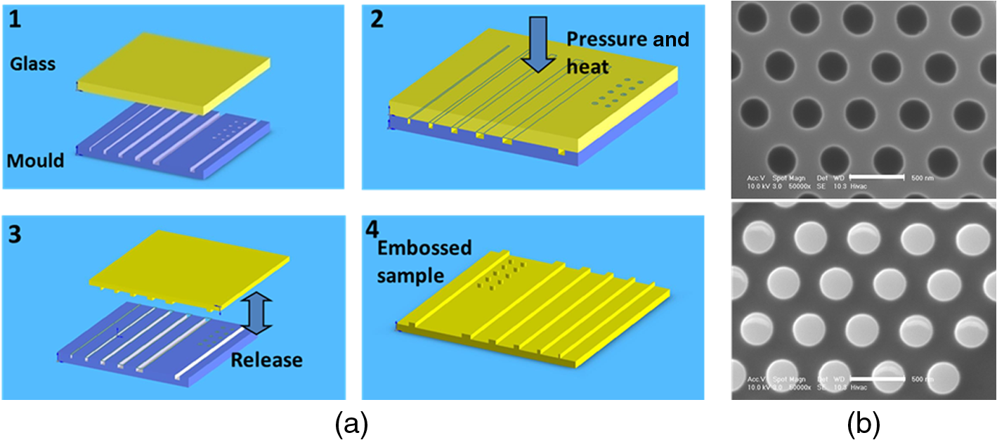 2.2.Patterning FidelityUsing a hard, silicon mold, the mold-fidelity of the patterning of hot-embossed chalcogenide glasses has been demonstrated to date to be at ca. 19,20 [Fig. 1(b)], but there is no reason why this cannot be improved. Surface roughness ultimately contributes to scattering loss in the waveguide and will affect the quality of the waveguide evanescent field interaction with the abutted analyte. A surface quality of ca. surface roughness for Si waveguides is achievable25 for use at telecommunication wavelengths. Bearing in mind that the most useful part of the mid-IR spectrum for detection of molecular species is - to 12-μm wavelength,1 then for mid-IR on-chip biosensors a larger surface roughness can be tolerated. Furthermore, the ultimate surface roughness depends primarily on the mold quality and as patterned silicon molds are useful here (oxidation at the silicon mold surface to silica renders it nonstick to chalcogenide glasses), there is potential for very low surface roughness after patterning. 3.Hot Embossing: Chalcogenide-on-ChalcogenideFor evanescent-field-mediated sensing, the top surface of the waveguide should be engineered to be an exposed waveguide core and hence air-clad so as subsequently to allow the analyte to be in close core contact during the sensing. For the hot embossing process, we have mainly used a lower refractive index bulk chalcogenide glass to function as both the substrate and optical under-cladding. The developed core/clad. pair of chalcogenide glasses are sufficiently matched in thermal properties (thermal expansion coefficient, viscosity/temperature relation) to allow thermal coprocessing. The closer in refractive index, the more likely it is that the core/cladding glasses will be amenable to thermal coprocessing because their chemical composition and molecular structure will be closer also. To test the approach, we rather selected a disparate refractive index pair exhibiting a high NA: with an As-Se core and Ge-As-Se acting as the under-cladding and substrate,19–24 (see Table 1); this pair has been used exclusively through our work in Refs. 19–23 and that has permitted us to compare more rigorously our hot embossing as the processing is modified. Table 1 highlights the key thermal properties when coprocessing two glasses using hot embossing with a hard mold. Here, As-Se core glass and Ge-As-Se under-cladding glass were selected to make high NA waveguides (Secs. 3.1–3.4) and Refs. 19–23. The key properties to control are: (i) avoidance of thermal expansion coefficient mismatch and (ii) of the under-cladding substrate core glass—this gives the possibility of selectively (de)forming the core glass but not the under-cladding substrate because the under-cladding substrate is more viscous at any temperature whereby: ( is the liquidus). Thus molding of the thermally deposited supercooled thin film above took place within a range of temperatures for which the substrate was at higher viscosity than the thin film.22 of the Ge-As-Se glass substrate was , which is higher than that of bulk glass (Ref. 21) (Table 1). Throughout the work, the Ge-As-Se substrates have been obtained by glass melting and then ground, polished, and finally pressed flat under a vacuum before use.20–24 The refractive index difference of the core/under-clad. pair has been sufficient to provide designs that were robust against the small process-induced uncertainty in actual refractive index. The NA was found to remain similar at longer wavelengths 22, which makes this pair suitable for forming high NA rib waveguides for both near- and mid-IR applications. Successful co-processing has been achieved using four different approaches: hot pressing fiber-on-glass (FOG); hot embossing of a thermally evaporated film (core glass) on glass, hot embossing of a radio frequency (RF) sputtered film on glass and also photolithography and dry etching, as follows in Secs. 3.1 to 3.4. Table 1Highlights key thermal properties when coprocessing two glasses using hot embossing. Here, As-Se core glass and Ge-As-Se under-cladding glass were selected to make high NA waveguides (Secs. 3.1–3.4) (Refs. 19–23). The key property is to avoid mismatch of thermal expansion coefficient while arranging for glass transition (Tg) of the under-cladding substrate to be above that of the core glass in order to have the possibility of (de)forming the core glass while the under-cladding substrate, being more viscous, remains undeformed.
3.1.Fiber-on-GlassFor the FOG processing,21 chalcogenide-glass monomode rib waveguides were fabricated by means of hot pressing using a patterned hard silicon mold [Fig. 2(a)]. As-Se fibers were aligned such that each fiber lay in one channel in the mold with sufficient separation between fibers. The polished, flattened (by hot pressing) Ge-As-Se substrate was placed on top of the fibers in the mold and hot pressing was carried out. During the hot pressing, the fiber spread to fill the proximate mold channels and adhered to the Ge-As-Se substrate. Fig. 2Hot embossing of fiber-on-glass (FOG). SEMs of: (a) Si mold cross section and (b) top view of As-Se ribs on the Ge-As-Se substrate, together with a cross-sectional view at higher magnification. (c) Near-field intensity profile observed at 1.55 μm. (Reprinted with permission from W. J. Pan et al., Microwave Opt. Technol. Lett., 50 (7), 1961–1963 (2008). Copyright [2008], Wiley.)21 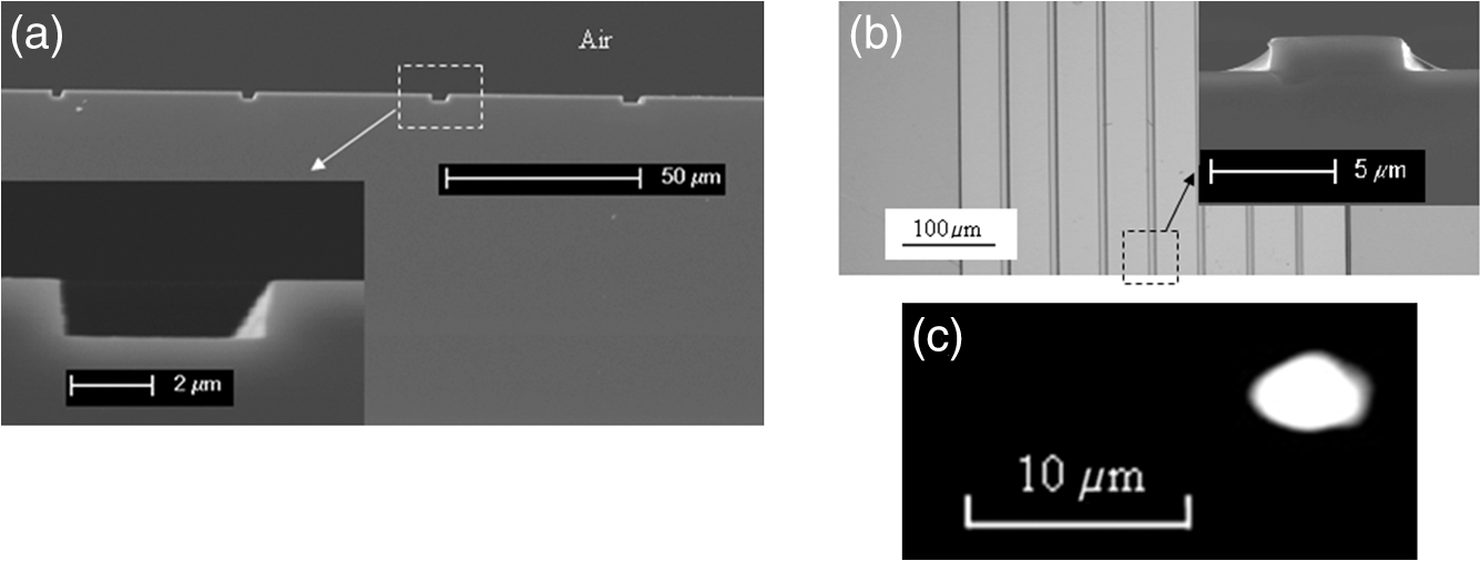 The one-step FOG approach produced waveguides comprised of . Designed for monomode operation, one of the waveguides was an As-Se rib core of 5-μm width and 1.7-μm depth [Fig. 2(b)]. The lowest recorded optical loss of the monomode waveguides was at 1550-nm wavelength and the near-field image confirmed monomode guiding [Fig. 2(c)].21 3.2.Thermally Evaporated Film on GlassThe second method we have used was to evaporate thermally an As-Se chalcogenide glass film onto a Ge-As-Se chalcogenide glass substrate.22 Hot embossing of the thermally evaporated thin As-Se film was carried out using a silicon mold to make the waveguides. An example shown in Fig. 3 is of a monomode guiding rib core: 5.5-μm wide and 1.9-μm deep. The lowest recorded optical loss for the monomode waveguides was at 1550 nm. The refractive indices of the core and under-cladding at 1550 nm were and , respectively.22 The waveguide exhibited excellent stability at ambient temperatures. Fig. 3For the As-Se thermally evaporated film on the pressed Ge-As-Se substrate: (a) refractive index dispersion from ellipsometry and (b) SEM backscattered image. (c) Near-field intensity profile (quasi-TE mode) at 1550 nm of a 5.5-μm wide As-Se rib waveguide on Ge-As-Se substrate. SEMs of: (d) cross-sectional and (e) plan view of an embossed As-Se waveguide on the Ge-As-Se substrate. (Reprinted with permission from Z. G. Lian et al., Opt. Lett. 34 (8), 1234–1236 (2009). Copyright [2009], OSA.)22 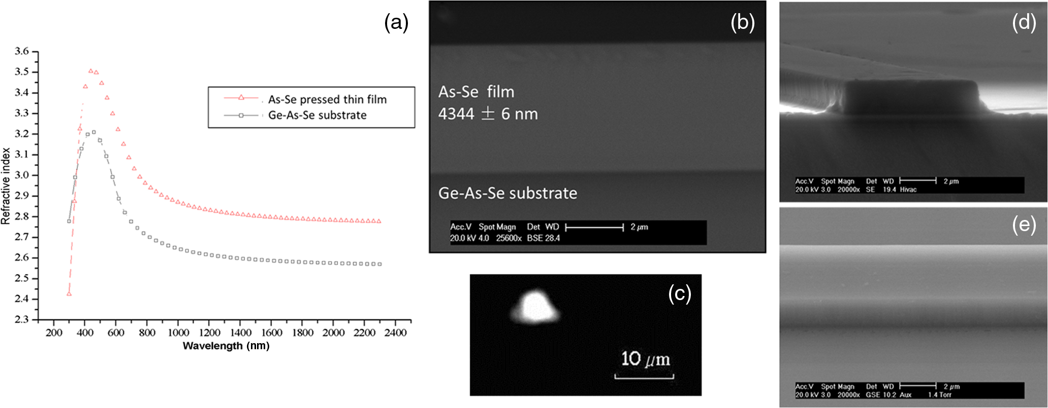 Advantages of thermal evaporation for depositing thin chalcogenide glass films include a relatively high deposition speed, but thermal evaporation can have difficulties in depositing materials with high melting points as well as multicomponent and/or composite materials with a large melting point difference between their constituents, where noncongruent evaporation usually occurs resulting in nonhomogeneous films.26 Zakery and Elliot27 explain that the thermal-evaporation method is not suitable for the accurate transfer of stoichiometry of multicomponent glass films. The Group of Pradel28 has developed a thermal coevaporation approach using different targets to lay down simultaneously single components to obtain amorphous films with multicomponent compositions. 3.3.RF-Sputtered Films on GlassA third method was to hot emboss rib waveguides in an As-Se film deposited using RF-magnetron sputtering on a Ge-As-Se glass substrate.23 Figure 4 shows an environmental scanning electron microscope (ESEM) image of the cleaved edge comprising an as-sputtered film of As-Se on a Ge-As-Se substrate. The nonvisible interface between the two chalcogenide compositions indicates a defect-free and well-adhered interface. The corresponding energy dispersive x-ray spectroscopy (EDX) line scan of the Ge, As, and Se elements across the interface allowed measurement of the sputtered film thickness, which was .23 Fig. 4ESEM cross-sectional image of a cleaved edge of a RF-sputtered As-Se thin film top of a Ge-As-Se substrate. The depth of the As-Se thin film was measured to be , and this depth is indicated by the double-headed arrow superimposed on the micrograph.23 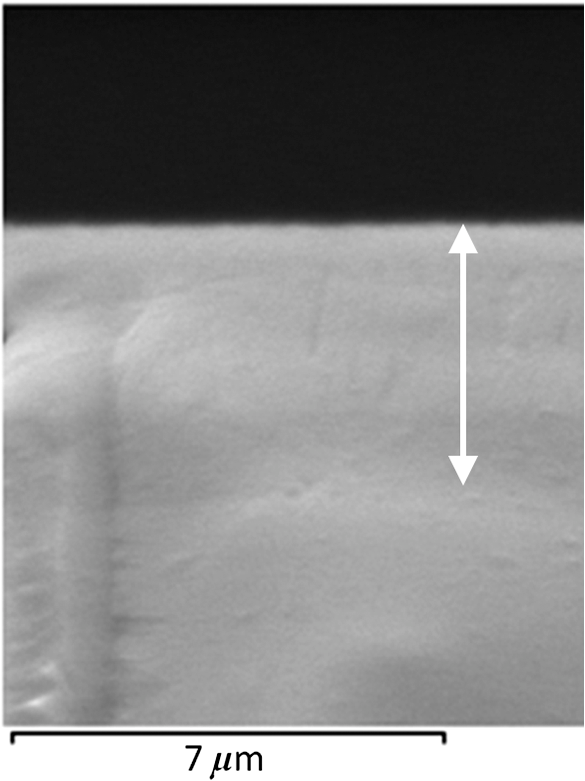 It has been previously reported29 that, unlike thermal evaporation, RF-sputtering can be responsible for the formation of column-like structures in deposited films. These column-like structures were detected, using atomic force microscopy, by Balan et al.29 in thin films of some chalcogenide multicomponent systems that had been deposited on unheated silicon and glass substrates. The refractive index of these films was also shown to decrease with the film thickness because of a change in the morphology (porosity) of the films with thickness.29 This columnar structure was explained29 in terms of the influence of deposition conditions, and in particular, the ratio of substrate temperature to thin film melting point (K).30 Furthermore, Balan et al.29 showed that, in general, multicomponent chalcogenide sputtered films of depth exhibited clustered-columns of approximate diameter 250 nm [confirmed by scanning electron microscopic (SEM) images], leading to a porosity estimated at and a measured decrease in refractive index of compared to depth films. As can be seen from Fig. 4 here, there was no apparent columnar structure present in ESEM micrographs of the RF-sputtered films collected for this work.23 Waveguides 4- to 6-μm wide and high were fabricated using hot embossing against a hard Si mold [Figs. 5(a) and 5(b)] and waveguide optical loss was measured using the Fabry-Perot technique [Figs. 6(a) and 6(b)]. Fig. 5SEM images of: (a) top view of As-Se glass ribs on Ge-As-Se glass substrate and (b) a cross-sectional view one of the ribs at higher magnification23 for hot embossed As-Se rib waveguides in an RF-sputtered As-Se film on a Ge-As-Se glass substrate. 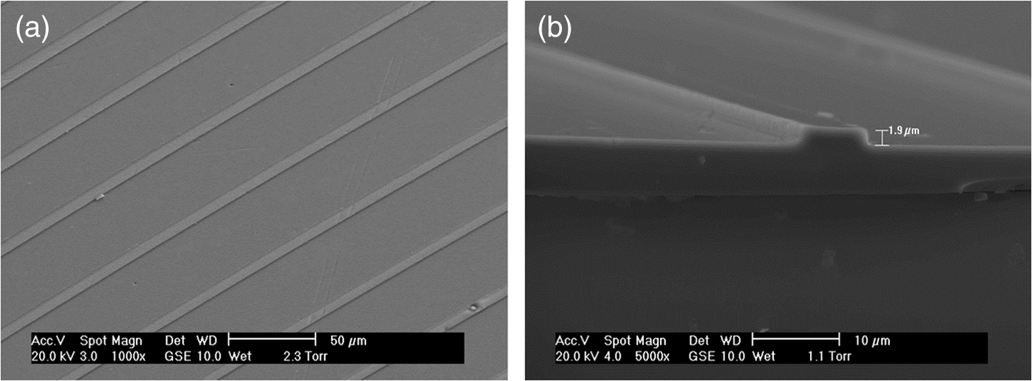 Fig. 6(a) Optical circuit used for measuring propagation loss; a soldering iron at 200°C was held over the top of the guiding rib and the maximum and minimum intensities of the resulting Fabry-Perot resonance were measured using a photodiode connected to a lock-in amplifier, connected in parallel with an optical chopper to a 150 Hz frequency generator and (b) (inset) near-field intensity profile observed at 1550-nm wavelength, quasi-TE mode, with horizontal line scan at maximum intensity of a 4.15-μm wide rib waveguide fitted to a Gaussian peak for hot embossed As-Se rib waveguides in a RF-sputtered As-Se film on a Ge-As-Se glass substrate.24 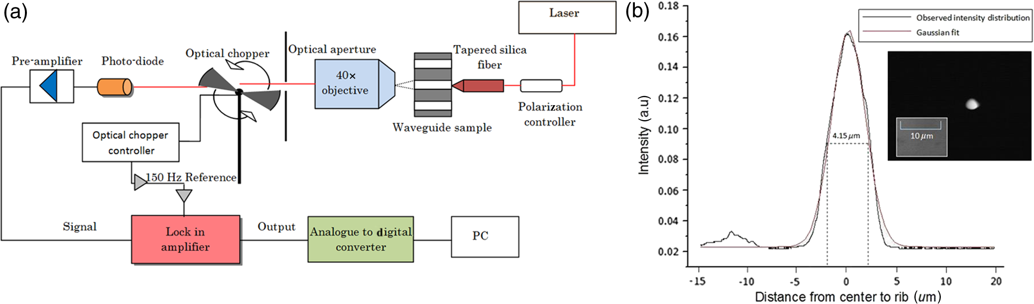 The Fabry-Perot method, which is known to overestimate loss [see Sec. 5, Fig. 6(a)], gave losses of for the transverse electric (TE) mode and for the transverse magnetic (TM) mode, at 1550-nm wavelength. Thus the waveguide loss was lower compared to both hot embossing with FOG (Sec. 3.1) and hot embossing a thermally evaporated As-Se glass thin film on a Ge-As-Se glass substrate (Sec. 3.2) (Table 2). Table 2Summary of the lowest recorded optical losses at 1550-nm wavelength for monomode As-Se glass rib waveguides on Ge-As-Se glass substrates. The rib waveguides were shaped via either hot embossing or dry etching and this shaping was carried out on either FOG or thermally evaporated, or RF-sputtered deposited, As-Se films on the Ge-As-Se glass substrate (Y=yes).
3.4.Mixed Approaches of Combined Plasma Etching and Hot EmbossingFollowing the work done by Choi et al.31 on etching thermally evaporated As-S films in a ( free) plasma, we have developed a similar inductively coupled plasma etching process.24 This was applied initially to etch rib structures in As-S bulk glass in order to repeat the Choi et al.31 results and standardize the procedures. After that, the dry etching process was applied to shape rib waveguides in As-Se thin films that had been either RF-sputtered onto silicate-glass microscope slides or RF-sputtered onto Ge-As-Se chalcogenide glass substrates.24 The lowest recorded loss was for a As-Se rib on Ge-As-Se glass substrate (see Fig. 7) and was for the quasi-TE mode and for the quasi-TM mode. Fig. 7SEM cross-sectional view of an As-Se rib waveguide 5.5-μm wide and 0.98-μm deep that had been shaped by dry etching of an RF-sputtered As-Se film on a Ge-As-Se substrate.24 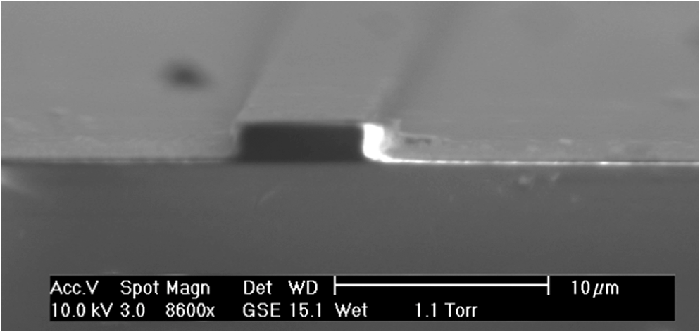 3.5.SummaryTable 2 summarizes the results in Secs. 3.1–3.4. From Table 2, optical loss results for the As-Se waveguides formed by dry etching of RF-sputtered films (ca. at 1550 nm) were higher than the loss obtained for the same design of As-Se waveguides but which had been instead shaped by hot embossing against a hard silicon mold (cf. ca. at 1550 nm). It is suggested that the extra loss found for the dry-etched As-Se waveguides compared to the hot embossed As-Se waveguides was associated with extra surface roughness. A comparison of the pros and cons of hot embossed waveguides (fast, cheap, scalable, surface roughness dependent on integrity of mold and thus repeatable fabrication of successive waveguides with the same mold, but could not, for instance, be repeated on same chip due to the temperature cycling this would incur) versus plasma-etched waveguides (expensive, many-step processing, repeatable fabrication of successive waveguides once have optimized process, masking would allow revisiting same chip for further shaping) suggests that there are various advantages and disadvantages of both types of waveguide processing. Moreover, it is concluded that their use in combination, whereby hot embossed waveguides could be postprocessed using plasma etching, offers the greatest versatility of approach for mid-IR photonic integration. 4.Glass Stability, Environmental and Photostability of Embossed Waveguides4.1.Glass Stability4.1.1.General commentsThe term glass stability refers to the ability of a glass to remain amorphous and not to devitrify (i.e., crystallize). This is important not only during waveguide manufacture but also in service. For chalcogenide glasses, so long as the operating temperature remains less than 50 K below , then no reflow of the material is expected to occur at normal pressure. However, at and above up to the liquidus, the material transforms to a supercooled liquid and, in thermodynamic terms, is therefore metastable with respect to the primary crystallizing phase. In the absence of heterogeneous nuclei, the kinetics of transformation from the supercooled liquid to the crystalline phase of chalcogenide glasses can be remarkably slow compared to, for example, the speed of this type of phase transformation of some of the metallic glasses and glasses, but is still at least an order of magnitude faster than devitrification rates of common multicomponent silicate glasses. The situation is worsened in the presence of heterogeneous nuclei (foreign material) and this is why very pure glasses should be used; also, heating the chalcogenide glasses in the presence of other materials should be attempted with caution. In addition, there have been reports of chalcogenide glasses devitrifying under the action of subbandgap light at ambient temperatures termed photocrystallization.32 Despite the potential for devitrification, the chalcogenide glasses are more likely to be limited during manufacture and use by problems of volatilization, oxidation, and hydrolysis above . 4.1.2.During manufactureWe have found excellent glass stability of the selenide-glass-based hot embossed waveguides during manufacture, use, and storage under ambient conditions. They remain amorphous according to x-ray diffractometry of the devices. Optical loss measurements have been demonstrated to remain constant for at least 3 weeks. This observed glass and rib-waveguide stability is in stark contrast to the results of some others for chalcogenide glass rib waveguides. Thus the group of Luther-Davies has reported postprocessing problems of crystallization of As-S rib waveguides which had been formed in thermally evaporated As-S films on a substrate of oxidized Si.33 In addition, Hu et al.34 reported that they coated thermally evaporated As-S with SU8 polymer to “prevent surface oxidation of devices in As-S.” Moreover, Hu et al.15 postheat-treated waveguides to “stabilize the glass structure.” Yet no such problems were reported when they applied similar processing to form Ge-Sb-S rib waveguides, in which, purposefully, no additional upper cladding layer was added.3 As an alternative explanation to crystallization by surface photooxidation of rib waveguides, formed in thermally evaporated films, Wang et al.35 have referred to a type of intrinsic phase separation in to explain crystallization of pulsed laser deposited films of , and this intrinsic phase separation is suggested to be present even in bulk glass itself, according to the ideas of Georgie et al.,36 but these ideas are not universally accepted. As eloquently reviewed by Nordman et al.,37 what is generally accepted is that thermally evaporated films inevitably contain molecular clusters, composed of both heteropolar bonds and homopolar “wrong” bonds, found in the vapor state itself, and that heat-treating can help to lower the prevalence of the “wrong bonds” and also densify thermally evaporated films to achieve more nearly the same refractive index as that of the parent bulk glass. From the above studies, it might be concluded that the thermal-evaporation process may be more problematic and that RF-sputtering might lead to more robust glass films. However, the observations of Balan et al.29 (see Sec. 3.3) that RF-sputtering can be responsible for the formation of column-like structures in thin chalcogenide glass films deposited on unheated silicon and glass substrates indicate that caution must be applied to both thermal evaporation and RF-sputtering methods of making chalcogenide films and film integrity cannot just be assumed. 4.2.Mechanical and Environmental (Including Photo-) StabilityThe chalcogenide glasses exhibit low phonon energies and hence mid-IR transparency precisely because they are based on weaker chemical bonding that silicate glasses. Because of the weaker chemical bonding, inevitably the chalcogenide glasses have both lower fracture stress and modulus of rupture than silicate glasses.38 Corrosion resistance of chalcogenide glasses to water vapor and liquid water at ambient temperatures is good, but strong alkalis and acids should be avoided. No photoinduced changes under ambient lighting conditions have been observed to date in our waveguides. Also in preliminary experiments, the resistance of RF-sputtered chalcogenide films to photodamage was apparently good for exposures of several minutes to fiber-coupled lasers, viz. 7 mW HeNe cw (651-nm wavelength); 40 mW cw 974 nm and 1320 nm diode lasers,24 i.e., the waveguide optical loss at 1.55 μm was unaffected by these exposures. But photodarkening of chalcogenide glasses is known to occur, as reported by Tanaka.39 5.Brief Comparison of Methods to Measure Waveguide LossThroughout the literature, there are several common methods to measure the optical loss of short optical waveguides. Each method has susceptibility to particular artifacts which tend artificially either to depress or to enhance loss. The most accurate method is the cut-back approach. This is commonly used for measuring the optical loss of optical fibers, for which long pathlengths are available. The cut-back method involves measuring the output light intensity from the exit face of the waveguide (), then keeping the same input conditions, the waveguide is “cut-back” (cleaved) to a shorter length(s) and the output intensity of light remeasured (). Loss in is calculated from the ratio of the two output intensities and the length cut-back () ().40 However, the shorter the waveguide, the more it is physically difficult to obtain a good cleave (whereby the cleave itself does not dominate the loss) and meaningful results. An alternative to this destructive cut-back approach is to fabricate waveguide sections of different length. The Fabry-Perot approach [see Fig. 5(a)], adopted by our Group, is a fundamental approach. The cavity length is changed by raising the temperature of the waveguide above ambient (it expands), we do this simply by holding a soldering-iron close. Here, the measured optical loss results tend to be higher than the actual. This is because the Fabry-Perot technique is concerned with measuring the round-trip loss inside the cavity of the waveguide. Due to the nature of the cleaving process, defects are expected on the cleaved end-faces of the waveguide and so the end-face modal reflectivity will be lower than the numerical values. Hence, the loss values quoted are regarded as an upper limit to the actual waveguide loss. The insertion loss can also be used as a measure of propagation loss. However, some assumptions must then be made about coupling losses and reflections, so giving rise to some uncertainty in the estimated loss. 6.Prospects for Hot Embossing for Mid-IR Chip Biosensors and Other Molecular SensorsTo date, there are limited reports of mid-IR (i.e., wavelength range 3 to 25 μm) integrated chip-sensors based on any waveguide material for evanescent field sensing. The chief reason holding back this technology is that such sensing cannot be fully exploited without readily available bright, discrete, and broadband mid-IR sources, of the appropriate output (wavelength matched to the vibrational absorption of the analyte), preferably on-chip. In the shorter wavelength, near-IR region (, ), evanescent field sensing has been demonstrated in an integrated chalcogenide glass slab waveguide.3 The chalcogenide glass waveguide consisted of exposed core of a 400-nm thick Ge-Sb-Se film on top of the oxidized Si; the waveguide loss was reported as at 1550 nm. These waveguides were successfully used in conjunction with microfluidics as a near-IR evanescent sensor device to detect the [N-H] vibrational absorption of N-methylaniline at 1500 nm. However, this near-IR N-H absorption is a weak overtone. Far stronger, fundamental vibrational absorption bands of [N-H] exist in the mid-IR beyond 3-μm wavelength for this molecule potentially giving better optical contrast of sensing and hence greater sensor sensitivity. So, mid-IR sensing is the way forward. The first steps of biofunctionalization of a planar chalcogenide sulfide waveguides have been demonstrated4 laying down a gold-coating on top of the waveguide, then the anchor molecules [1,1-mercaptoundecanoic acid (MUA)] were hooked on the gold to form SAMs (self-assembly monolayers) onto which antibodies could be attached. But, such biofuntionalization of waveguides is unnecessary for waveguide sensing in the mid-IR because mid-IR molecular detection is direct. A true mid-IR on-chip sensor has been demonstrated by Chang et al. comprising on-chip mid-IR evanescent field sensing of cocaine.41 The waveguide in this case was a germanium (Ge) strip waveguide on a silicon (Si) substrate integrated with a microfluidics to detect cocaine in tetrachloroethylene solutions. In the evanescent field of the waveguide, cocaine exhibited characteristic vibrational absorption at , and the quantum cascade laser (QCL) mid-IR source was matched to that wavelength. The QCL was off-chip. Chalcogenide glass rib waveguides would be suitable for this application and could substitute the Ge waveguide for sensing a plethora of molecules. But the limitation is the availability of QCLs operating at the correct wavelength to match the characteristic molecular absorptions. To truly open up the field of mid-IR integrated evanescent field sensors, bright broadband mid-IR on-chip sources are now required and short supercontinuum source devices are attractive for this.6 7.ConclusionsThis paper has demonstrated that low optical loss, mid-IR chalcogenide-glass waveguides can be readily fabricated via the hot-embossing technique; the processing is fast, scalable, and obviates the need for expensive equipment. On the other hand, conventional photolithography and dry etching are also successful in making chalcogenide glass integrated photonic circuitry. The two techniques combined together present a substantial versatile approach and a gateway to photonic integration on-chip. An open-core chalcogenide glass rib waveguide is a simple format to integrate with microfluidics. The microfluidic channel brings molecular liquids or solutions into close proximity with the waveguide for evanescent-field detection of the vibrational absorption of the abutted molecular analyte. Similarly molecular gases and solids can be brought into proximity of the waveguide for mid-IR evanescent-field detection. What is now needed is new bright, mid-IR broadband sources on-chip. QCLs operating in the mid-IR can provide sufficient brightness for mid-IR evanescent field sensing; they are suitable as on-chip, discrete, bright mid-IR sources but limited in wavelength range. Short SCG waveguide or taper sources are exceedingly attractive as on-chip, broadband, bright mid-IR sources to enable detection of characteristic spectral absorptions across the mid-IR, to bring about unambiguous identification and quantification of molecular analytes. AcknowledgmentsW.J.P. and Z.G.L. are grateful to the University of Nottingham for their PhD Scholarships. Grant CZ.1.07/2.3.00/20/0254 realized by the European Science Foundation (ESF) and the Ministry of Education, Youth, and Sports of the Czech Republic. ReferencesA. B. Seddon,
“A prospective for new mid-infrared medical endoscopy using chalcogenide glasses,”
Int. J. Appl. Glass Sci., 2
(3), 177
–191
(2011). http://dx.doi.org/10.1111/j.2041-1294.2011.00059.x IJAGD4 2041-1294 Google Scholar
G. E. Snopatinet al.,
“High-purity chalcogenide glasses for fiber optics,”
Inorg. Mater., 45
(13), 1439
–1460
(2009). http://dx.doi.org/10.1134/S0020168509130019 INOMAF 0020-1685 Google Scholar
J. Huet al.,
“Fabrication and testing of planar chalcogenide waveguide integrated microfluidic sensor,”
Opt. Express, 15
(5), 2307
–2314
(2007). http://dx.doi.org/10.1364/OE.15.002307 OPEXFF 1094-4087 Google Scholar
M.-L. Anneet al.,
“Chalcogenide glass optical waveguides for infrared biosensing,”
Sensors, 9
(9), 7398
–7411
(2009). http://dx.doi.org/10.3390/s90907398 SNSRES 0746-9462 Google Scholar
Y. Zouet al.,
“Thermal nanoimprint fabrication of chalcogenide glass waveguide resonators,”
in OSA Proc. CLEO: Science and Innovations, Fabrications and Applications,
(2013). http://dx.doi.org/10.1364/CLEO.SI.2013.cTh1J.5 Google Scholar
Y. Yuet al.,
“Mid-infrared supercontinuum generation in chalcogenides,”
Opt. Mater. Exp., 3
(8), 1076
–1086
(2013). http://dx.doi.org/10.1364/OME.3.001075 OMEPAX 2159-3930 Google Scholar
M. Frumaret al.,
“Thin chalcogenide films prepared by pulsed laser deposition—new amorphous materials applicable in optoelectronics and chemical sensors,”
J. Non-Cryst. Solids, 352
(6–7), 544
–561
(2006). http://dx.doi.org/10.1016/j.jnoncrysol.2005.11.043 JNCSBJ 0022-3093 Google Scholar
W. C. Liuet al.,
“Slab waveguides and nanoscale patterning of pulsed laser-deposited Ge 0.2 Se 0.8 chalcogenide films,”
Appl. Phys. Lett., 93
(4), 041107
(2008). http://dx.doi.org/10.1063/1.2965124 APPLAB 0003-6951 Google Scholar
A. Zakery,
“Low loss waveguides in pulsed laser deposited arsenic sulfide chalcogenide films,”
J. Phys. D: Appl. Phys., 35
(22), 2909
–2913
(2002). http://dx.doi.org/10.1088/0022-3727/35/22/304 JPAPBE 0022-3727 Google Scholar
X. Gaiet al.,
“Progress in optical waveguides fabricated from chalcogenide glasses,”
Opt. Exp., 18
(25), 26635
–26646
(2010). http://dx.doi.org/10.1364/OE.18.026635 OPEXFF 1094-4087 Google Scholar
C. VigreuxA. Pradel,
“Chalcogenide films for infrared integrated optics,”
Proc. SPIE, 7218 721802
(2009). http://dx.doi.org/10.1117/12.807594 PSISDG 0277-786X Google Scholar
J.-F. Vienset al.,
“Fabrication and characterization of integrated optical waveguides in sulfide chalcogenide glasses,”
J. Lightwave Technol., 17
(7), 1184
–1191
(1999). http://dx.doi.org/10.1109/50.774252 JLTEDG 0733-8724 Google Scholar
A. Ganjooet al.,
“Planar chalcogenide glass waveguides for IR evanescent wave sensors,”
J. Non-Cryst. Solids, 352
(6–7), 584
–588
(2006). http://dx.doi.org/10.1016/j.jnoncrysol.2005.12.010 JNCSBJ 0022-3093 Google Scholar
J. Huet al.,
“Si-CMOS-compatible lift-off fabrication of low-loss planar chalcogenide waveguides,”
Opt. Exp., 15
(19), 11798
–11807
(2007). http://dx.doi.org/10.1364/OE.15.011798 OPEXFF 1094-4087 Google Scholar
J. Huet al.,
“Optical loss reduction in high-index-contrast chalcogenide glass waveguides via thermal reflow,”
Opt. Exp., 18
(2), 1469
–1478
(2010). http://dx.doi.org/10.1364/OE.18.001469 OPEXFF 1094-4087 Google Scholar
Y. ZhaM. WaldmannC. B. Arnold,
“A review on solution processing of chalcogenide glasses for optical components,”
Opt. Mater. Exp., 3
(9), 1259
–1272
(2013). http://dx.doi.org/10.1364/OME.3.001259 OMEPAX 2159-3930 Google Scholar
Q. Coulombieret al.,
“Planar waveguide obtained by burying a Ge22As20Se58 fiber in As2S3 glass,”
Appl. Opt., 47
(31), 5750
–5752
(2008). http://dx.doi.org/10.1364/AO.47.005750 APOPAI 0003-6935 Google Scholar
E. Romanovaet al.,
“Non-linear chalcogenide glasses and technologies for the development of ultra-fast chip-scale optical devices,”
in Proc. ICTON IEEE,
256
–259
(2008). Google Scholar
A. B. Seddonet al.,
“Fine embossing of chalcogenide glasses—a new fabrication route for photonic integrated circuits,”
J. Non-Cryst. Solids, 352
(23–25), 2515
–2520
(2006). http://dx.doi.org/10.1016/j.jnoncrysol.2006.03.025 JNCSBJ 0022-3093 Google Scholar
W. J. Panet al.,
“Fine embossing of chalcogenide glasses: first time submicron definition of surface embossed features,”
J. Non-Cryst. Solids, 353
(13–15), 1302
–1306
(2007). http://dx.doi.org/10.1016/j.jnoncrysol.2006.10.077 JNCSBJ 0022-3093 Google Scholar
W. J. Panet al.,
“One-step hot embossing of optical rib waveguides in chalcogenide glasses,”
Microwave Opt. Technol. Lett., 50
(7), 1961
–1963
(2008). http://dx.doi.org/10.1002/(ISSN)1098-2760 MOTLEO 0895-2477 Google Scholar
Z. G. Lianet al.,
“Embossing of chalcogenide glasses: monomode rib optical waveguides in evaporated thin films,”
Opt. Lett., 34
(8), 1234
–1236
(2009). http://dx.doi.org/10.1364/OL.34.001234 OPLEDP 0146-9592 Google Scholar
N. S. Abdel-Moneimet al.,
“Fabrication of stable, low optical loss rib-waveguides via embossing of sputtered chalcogenide glass-film on glass-chip,”
Opt. Quantum Electron.,
(2014). http://dx.doi.org/10.1007/s11082-014-9917-z OQELDI 0306-8919 Google Scholar
N. A. Moneim,
“Fabrication of planar optical components in chalcogenide glasses,”
(2013). Google Scholar
A. B. Seddon,
“Chalcogenide glasses: a review of their preparation, properties and applications,”
J. Non-Cryst. Solids, 184 44
–50
(1995). http://dx.doi.org/10.1016/0022-3093(94)00686-5 JNCSBJ 0022-3093 Google Scholar
A. ZakeryS. R. Elliott, Optical Nonlinearities in Chalcogenide Glasses and Their Applications, Springer-Verlag, Berlin-Heidelberg
(2007). Google Scholar
A. A. Piarristeguyet al.,
“Glass formation in the GexTe100-x binary system: synthesis by twin roller quenching and co-thermal evaporation techniques,”
J. Non-Cryst. Solids, 355
(37), 2088
–2091
(2009). http://dx.doi.org/10.1016/j.jnoncrysol.2009.04.072 JNCSBJ 0022-3093 Google Scholar
V. BalanC. VigreuxA. Pradel,
“Chalcogenide thin films deposited by radio-frequency sputtering,”
J. Optoelectron. Adv. Mater., 6
(3), 875
–882
(2004). 1454-4164 Google Scholar
J. A. Thornton,
“Influence of apparatus geometry and deposition conditions on the structure and topology of thick sputtered coatings,”
J. Vac. Sci. Technol., 11
(4), 666
–670
(1974). http://dx.doi.org/10.1116/1.1312732 JVSTAL 0022-5355 Google Scholar
D.-Y. Choiet al.,
“Dry etching characteristics of amorphous As2S3 film in plasma,”
J. Appl. Phys., 104
(11), 113305
(2008). http://dx.doi.org/10.1063/1.3041647 JAPIAU 0021-8979 Google Scholar
A. E. OwenP. J. S. Euen, High Performance Glasses, Blackie, London
(1992). Google Scholar
D.-Y. Choiet al.,
“SU-8 protective layer in photo-resist patterning on As2S3 film,”
Phys. Stat. Solidi, C8
(11–12), 3183
–3186
(2011). http://dx.doi.org/10.1002/pssc.201000741 PHSSAK 0031-8957 Google Scholar
J. Huet al.,
“Planar waveguide-coupled, high-index-contrast, high-Q resonators in chalcogenide glass for sensing,”
Opt. Lett., 33
(21), 2500
–2502
(2008). http://dx.doi.org/10.1364/OL.33.002500 OPLEDP 0146-9592 Google Scholar
R. P. Wanget al.,
“Annealing induced phase transformations in amorphous As2S3 films,”
J. Appl. Phys., 100 063524
(2006). http://dx.doi.org/10.1063/1.2353787 JAPIAU 0021-8979 Google Scholar
D. G. GeorgieP. BoolchandK. A. Jackson,
“Intrinsic nanoscale phase separation of bulk As2S3 glass,”
Philos. Mag., 83
(25), 2941
–2953
(2003). http://dx.doi.org/10.1080/1478643031000151196 PMHABF 1478-6435 Google Scholar
O. NordmanN. NordmanN. Peyghambarian,
“Electron beam induced changes in refractive index and film thickness of amorphous AsxS100-x and AsxSe100-x films,”
J. Appl. Phys., 84
(11), 6055
–6058
(1998). http://dx.doi.org/10.1063/1.368915 JAPIAU 0021-8979 Google Scholar
J. S. Sanghera, , Young’s modulus of chalcogenide glasses is that of silica glass and the mechanical properties of chalcogenide glasses in general appear to be down by this factor relative to silica glass, private communication (2010).J. S. Sanghera, , Young’s modulus of chalcogenide glasses is that of silica glass and the mechanical properties of chalcogenide glasses in general appear to be down by this factor relative to silica glass, private communication (2010). K. Tanaka,
“Configurational and structural models for photo-darkening in glassy chalcogenides,”
J. Appl. Phys., 25
(Part 1, 6), 779
–786
(1986). http://dx.doi.org/10.1143/JJAP.25.779 JAPIAU 0021-8979 Google Scholar
A. BornsteinN. CroitoruE. Marom,
“Chalcogenide infrared As2-xSe3+x glass fibers,”
J. Non-Cryst. Solids, 74
(54), 57
–65
(1985). http://dx.doi.org/10.1016/0022-3093(85)90400-4 JNCSBJ 0022-3093 Google Scholar
Y.-C. Changet al.,
“Cocaine detection by a mid-infrared waveguide integrated with a microfluidic chip,”
Lab Chip, 12
(17), 3020
–3023
(2012). http://dx.doi.org/10.1039/c2lc40601b LCAHAM 1473-0197 Google Scholar
BiographyAngela B. Seddon leads the mid-infrared photonics group at the University of Nottingham, with world-class facilities for fabricating midinfrared fiber-optics and chips. Her major aim is to create a new paradigm in real-time mid-infrared medical sensing, imaging, and endoscopy for early, fast, and reliable medical diagnosis. She is an author of 220 publications and five book chapters. She is a fellow of the Royal Society of Chemistry, a fellow of the Society of Glass Technology, and a fellow of SPIE. Nabil S. Abdel-Moneim was educated in Egypt and carried out his master of engineering undergraduate degree in electronic and communication engineering at the University of Nottingham, England. He was awarded a full UK-India Initiative in Education and Research PhD scholarship, graduating in 2013 again at Nottingham. His PhD concerned fabrication of chalcogenide glass based optical components. He is currently a lecturer in Cairo. Lian Zhang received his BEng degree (with first class honors) in electronic and electrical engineering and PhD in chalcogenide glass devices from the University of Nottingham, England, in 2006 and 2010, respectively. Then, he joined the Optoelectronics Research Centre, University of Southampton as a postdoctoral research fellow. His current research interests include fabrication and characterization of microstructured optical fibers, based on variety of compound glasses. Wei J. Pan was awarded a PhD from the University of Nottingham, England, in 2008, where his work included some pioneering research on the applications of hot embossing for fabricating optical waveguides based on chalcogenide glasses. He is now a vice president at Algorithmic Trading and Execution team, Bank of America Merrill Lynch, Hong Kong. David Furniss graduated in physics from the University of Sheffield, England, in 1985 and continued there, achieving a PhD in 1989 in electronic paramagnetic resonance of rare earth ion doped glasses. Since then he has been a senior research fellow/officer at the Universities of Sheffield and Nottingham, moving to the University of Nottingham, England, in 2001. His research interests include pioneering methods of shaping mid-infrared glasses and optimizing their passive and active optical properties. Christopher J. Mellor graduated with a PhD degree in physics from the University of Birmingham, England, in 1986. He is currently associate professor and reader in physics at the School of Physics and Astronomy, the University of Nottingham, England. His research interests include nanofabrication, integrated optical components, nanomechanical systems, and scanning probe microscopy. He is the author of more than 70 publications in peer-reviewed journals. Tomas Kohoutek is a research fellow in the Department of General and Inorganic Chemistry at the University of Pardubice, Czech Republic. His research interests include solution processing of amorphous and crystalline semiconducting chalcogenides, physical-chemical properties of chalcogenide glasses, thin films, optical fibers, and photonic crystals. He obtained his PhD degree from the University of Pardubice, Czech Republic, in 2007. Jiri Orava is a research associate in the Department of Materials Science and Metallurgy at the University of Cambridge, UK, and the Advanced Institute for Materials Research, Tohoku University, Japan. His research interests include the synthesis and physical-chemical properties of chalcogenide glasses, photonic structures, and the optical and electrical data recording in amorphous semiconducting chalcogenides. He obtained his PhD degree from the University of Pardubice, Czech Republic, in 2009. Tomas Wagner, CSc, University of Pardubice, has been studying amorphous chalcogenides for more than 10 years. His interests cover inorganic chemistry, materials engineering, solid state chemistry, semiconducting materials, preparation and properties of amorphous and glassy chalcogenides, photostructural effects, physical and chemical methods of thin films preparations, thermal analysis (modulated differential scanning calorimetry, photocalorimetry), x-ray fluorescence analysis, spectroscopic ellipsometry, micro-optics, and phase change memories. He is an author or coauthor more than 165 refereed journal papers. Trevor M. Benson is professor in optoelectronics and director of the George Green Institute for Electromagnetics Research at the University of Nottingham, England. His research interests include experimental and numerical studies of electromagnetic fields and waves, with particular emphasis on the optical waveguides, lasers and amplifiers, and electromagnetic compatibility. He is a fellow of the Institute of Engineering Technology, the Institute of Physics, and the Royal Academy of Engineering. |
|||||||||||||||||||||||||||||||||||||||||||||||


