|
|
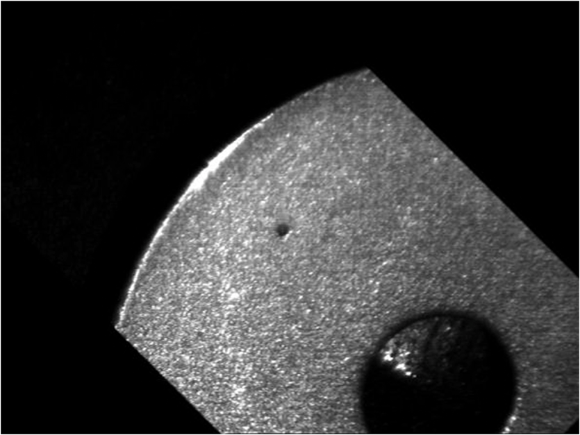
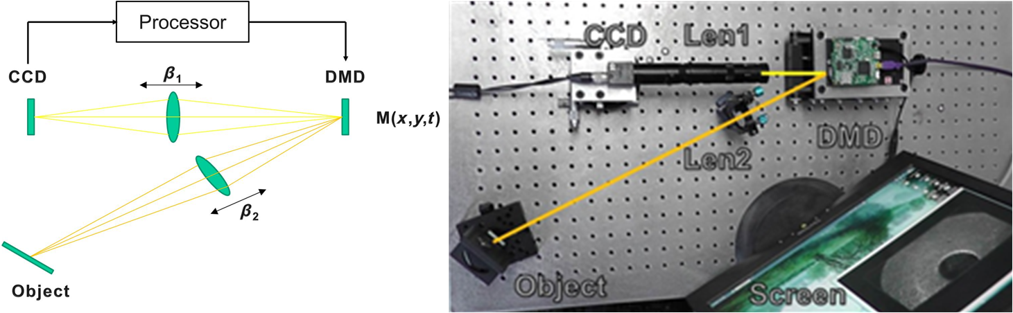
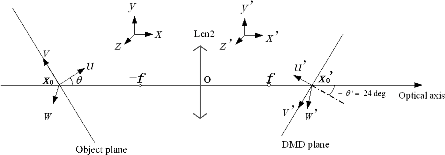
1.IntroductionVisual inspection for a highly reflective surface is commonly faced with a serious limitation which is that useful information on geometric construction and textural defects is covered by a blur due to specular highlights. With saturating corresponding charge coupled device (CCD) pixels, strong highlights increase the gray value of neighbors in an imaging sensor. The aforementioned phenomenon that reduces contrast and causes image blur is a parasitic image. In the visual system, a parasitic image arises from direct lights on a highly reflective surface (solid line with arrow), scattering glare in the lens element (dash and dot line), stray lights in the camera body (short dash line), and reflection off the lens surface (long dash line), as shown in Fig. 1. In our experiment, these sources causing a parasitic image are mainly scattering glare and direct light. The sum of the two sources saturates image point and increases the light intensity of its surrounding pixels. As shown in Fig. 2, scattering glare, which appears as a parasitic image, obscures the edge of the metallic slice in the presence of highlights. Therefore, it is necessary to remove the parasitic image created by specular highlights and capture realistic scenes. Fig. 1Schematic of parasitic image formation. (a) A highlight point could contribute to direct lights (solid line with arrow), scattering glare (dash and dot line), stray lights in camera body (short dash line), and reflection off lens surface (long dash line). (b) The sum of direct light and scattering glare saturates image point and increases light intensity of its surrounding pixels. 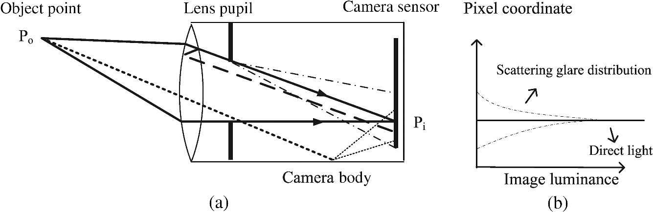 Many specularity removal techniques have been proposed: color space analysis; neighborhood analysis; polarization; image sequences (IS); multiple-flash images, etc.1–8 However, when scattering glare is in the neighboring region, these techniques are no longer valid. There are many methods to remove various parasitic images. Jaehyun et al.9 propose a multiexposure image fusion algorithm without a ghost effect. Schechner et al.7 introduce an approach that can avoid saturation of highlights and improve the quality of such images, in which multiple light sources simultaneously illuminate the object from different directions. Agrawal et al.8 present a novel gradient projection scheme that allows removal of reflections and highlights from flash images and uses a flash image and ambient image pair to produce better flash images. Bitlis et al.10 propose a shift variant analytical parametric model to reduce stray light effects in a digital camera. Liebe et al.11 analyze sun-induced veiling glare. These methods can be broadly classified as illumination techniques, multiexposure imaging, high dynamic range (HDR) camera, and a software algorithm. Multiexposure imaging will take a long time to implement photometric evaluation, spectral calibrations, and image reconstruction.12 Illumination strategies, which are complex and various, cannot always completely acquire full information of the measured work piece. Although an HDR camera can be used to raise the saturation point by increasing the capacity of the sensor electron well, producing large sensors is excessively expensive and reduces sensor resolution. On average, only a small portion of a scene contains strong highlights and therefore needs high capacity sensors. Software algorithms postprocess an image that already contains parasitic components. As the highlight due to the specular reflection of a metallic slice is very strong, the performance of software algorithms is poor. This article is inspired by previous works on computational camera as follows. Nayar et al.13 describe a programmable imaging system that uses a digital micromirror device (DMD) to alter the geometric and radiometric characteristics. Ri et al.14 propose phase-measuring profilometry using a DMD camera to extend the intensity range. Ankit et al.15 present an optical relay system for mechanical or electronic color spectrum control that utilizes a DMD in the optical path to modulate space lights. Adeyemi et al.16 demonstrate a system that uses precise DMD control of the projector to enhance the dynamic range. In this article, we have implemented a programmable imaging system that goes by the name of DMD Camera. A method for removal of a parasitic image and elimination of high reflection based on the DMD camera is presented. With this system, we can decrease the intensity of a scene ray based on the needs of the application before it reaches the imaging optics. This article explains the space light modulation (SLM) strategy for inspection of a metallic slice in detail. Finally, we demonstrate the effectiveness of a correction image and a parasitic image. 2.Prototype SystemHere, we describe programmable imaging system with a micromirror array. The system is composed of a CCD, DMD, image processor, and two imaging lenses (Len1 and Len2), as shown in Fig. 3. To avoid unexpected stray light caused by devices ahead of the DMD, the optical system is open. DMD is a two-dimensional (2-D) array optoelectronic element in which every pixel has two stable mirror states ( tilt and tilt) to control the direction of the scene ray with high precision over space and time. A PC, as the imaging processor, handles the camera image and controls the DMD pattern. The object, which is a Neodymium magnet slice in this article, is imaged at the DMD plane by Len2. Len1 focuses the reflected ray from the DMD to the CCD plane. The DMD, mounted on the intersection of two optical axes, modulates the incident ray from the object and reflects the processed ray to the CCD by 24-deg. Based on the working principle of the DMD, the reflected ray from the DMD is produced by pulse width modulating the mirror elements over the operating refresh time. Thus, the reflected intensity gray level is proportional to the period of time that the mirror is on tilt state. As the CCD receives different exposure times, the object image will be modulated by the DMD. 2.1.Mapping from Digital Micromirror Device to Charge Coupled DeviceThe DMD and CCD are both perpendicular to the primary optical axis of Len1 that is composed of five lenses. denotes paraxial magnification of Len1 from 0.5 to 2. Note that there are three possibilities for mapping from DMD to CCD: one DMD pixel being assigned to multiple CCD pixels, one DMD pixel being assigned to one CCD pixel, and multiple DMD pixels being assigned to one CCD pixel. The mapping of one DMD pixel being assigned to one CCD pixel is implemented in this article. Pixel-to-pixel correspondence is accurately adjusted by utilizing Shien’s method.17 The mapping has three steps as follows: first, we can control the DMD to display a checkerboard pattern. These corner coordinates of the checkerboard are already known. Second, the CCD captures the corresponding image corners which are imaged by Len1. Finally, the camera matrix , which represents a spatial relationship between the CCD and DMD, is calculated by utilizing RANSAC algorithm. The threshold value for determining when a datum fits a model is set by 0.05 pixels. 2.2.Mapping from Object to Digital Micromirror DeviceUsing the thin lens, an arbitrary plane in the object space will be imaged to a corresponding plane in the image space. The object plane is expressed as , where is the intersection point of the object plane and optical axis, thus we obtain an image plane: In Fig. 4, the object space coordinate system is defined by the intersection point of the object plane and optical axis which is taken as the origin, the -axis which is taken to be vertical, the -axis which is taken to be horizontal, and the -axis which parallels the normal vector of the object image. The image space coordinate system is defined by the intersection point of the DMD plane and optical axis which is taken as the origin, the -axis which is taken to be vertical, the -axis which is taken to be horizontal, and the -axis which parallels the normal vector of the DMD image. The angle between and the optical axis is expressed as . In the same way, the angle between and the optical axis is expressed as . The relationship between and can be written as . is the incident angle in the DMD plane and is set to 24 deg to insure that the reflected angle is 0 deg. Thus, it can be seen that is only associated with which is the measurement distance when the focal length of Len2 is invariant. The mapping of Len2 from a 2-D point in the image plane to a 2-D point in the object plane is given by where is the magnification factor of Len2. It is thus clear that the coordinate conversion between the image plane and the object plane conforms to a strictly linear mapping. Hence, the view magnification of the DMD camera can be expressed as . As is invariant in our experiment, the view magnification of the DMD camera is decided by the focal length of Len2 and the measurement distance.2.3.Experimental SetupThe CCD in our experiment allows for 8 bits per pixel (bpp) of precision in the RAW mode and a resolution of ; each CCD is in size. The DMD provides 8 bpp and a resolution of ; each mirror element is . Len1 is set to a paraxial magnification of 1.12. After mapping from the DMD to the CCD, our DMD camera has 200,000 effective pixels. The focal length of Len2 is 100 mm. The object distance and field of view (FOV) of this optical system is determined by the distance between Len2 and the DMD. 3.Removing Parasitic Image3.1.Point Spread FunctionAs shown in Fig. 1(b), the sum of direct light and scattering glare saturates image point and increases the light intensity of its surrounding pixels. Scattering glare falls off rapidly away from the central point source. Direct light and a part of scattering glare near the central point source are high frequency components. However, another part of scattering glare far away from bright sources is low frequency component. Intensity distribution of the parasitic image is usually described by a point spread function (PSF), which is a function of the distance from the central point source. Based on statistical observation, the PSF caused by strong highlights due to specular reflection takes this form: where is associated with the amplitude of direct light, and it is invariable for a central point source. is a coefficient of the point spread. The smaller value of is, the lower the intensity of scattering glare is, and the shorter the radius relative to the spread region is. is the position of the central point source. When incoming rays have an angular variation, the PSF is rewritten as where is the angle between the optical axis and incoming rays. is the radius relative to the central point source.3.2.StrategyWe assume that is the intensity of the recorded image which is composed of a correction image and a parasitic image . In our camera system, the result of processing a captured image can be fed again into the DMD as a pattern, and this process could be repeated. So far as the DMD is concerned, the relationship between the incident intensity and reflected intensity is obtained by using an optical power meter. From Eq. (3), one can observe that is linearly modulated by the DMD, but is not. Based on this property, the process of the experiment, which achieves a set of recorded image , is described as follows:
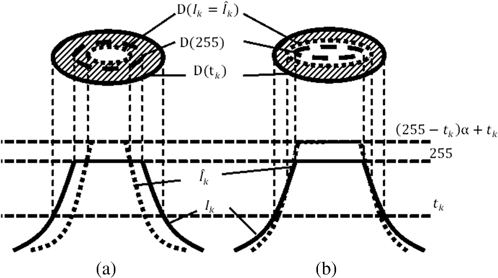
Considering the maximum possible brightness value of the CCD intensity level, there are two cases of solving a parasitic image, to be described in Fig. 5. Solid and dotted curves represent intensities of and , respectively. Also, the scattering glare is marked by hachures. In Fig. 5(a), the region of glare is enclosed between the boundary lines of and with the condition that the boundary dash line of is outside the boundary of . In Fig. 5(b), the region of glare is enclosed between the boundary lines of and with the condition that the boundary dash line of is inside the boundary of . With the condition that the dash line of is inside the boundary of , we can obtain the estimate of the parasitic image: where means the weight of . It is a relational function containing and the reflectivity of the DMD.That is a necessary condition of global parasitic image: Therefore, all selected thresholds in the experiment should be equal: With another case where the dash line of is outside the boundary of , we can obtain the estimate of the parasitic image: That is a necessary condition of the global parasitic image: Therefore, all selected thresholds in the experiment should be a monotone decreasing sequence: From Eq. (5), we composite the individual subtracted captures together to form a complete image of the scene: DMD enables radiometric modulation of the imaged scene rays with very high precision and physically limits the amount of scattering glare created in the camera. Also, with the highlight intensity falling off, signal-to-noise ratios (SNRs) are increasing. A large allows minimizing the highlight and increasing SNR, whereas IS is needed to record a global scene. It is suggested that the regions need to be as large as possible. This creates a tradeoff between the SNR and the integrity of the estimated parasitic image. Based on empirical observation, is suitable for our experiment. 4.Implementation ResultsWe provide two examples showing the successful application of the proposed method. The object is mounted on the working scene of a DMD camera in a dark room. Projecting lights illuminate the object from a constant angle from the right side. One example is the removal of parasitic image on metal slice, as shown in Fig. 2. It can be observed that high reflective light due to specular reflection, produces the parasitic image on the left edge of the metallic slice and covers the geometric and textural information of the metallic edge which is the stamping region in the fabrication process. Removing the parasitic image by using the preceding strategy, a correction image is given in Fig. 6. Figure 6(a) shows the recorded image where the edge of the metallic slice is covered by the parasitic image. Figure 6(b) shows the correction image where the parasitic image is removed by our approach. Notice that the edge of the metallic slice is visible. Figure 6(c) shows the parasitic image that is recovered. Figure 6(d) depicts the 2-D luminance distribution of the parasitic image superimposed by the central point sources and spreading components. Fig. 6A close-up of experimental result: (a) record image, (b) correction image, (c) parasitic image, and (d) a close-up of parasitic intensity distribution. 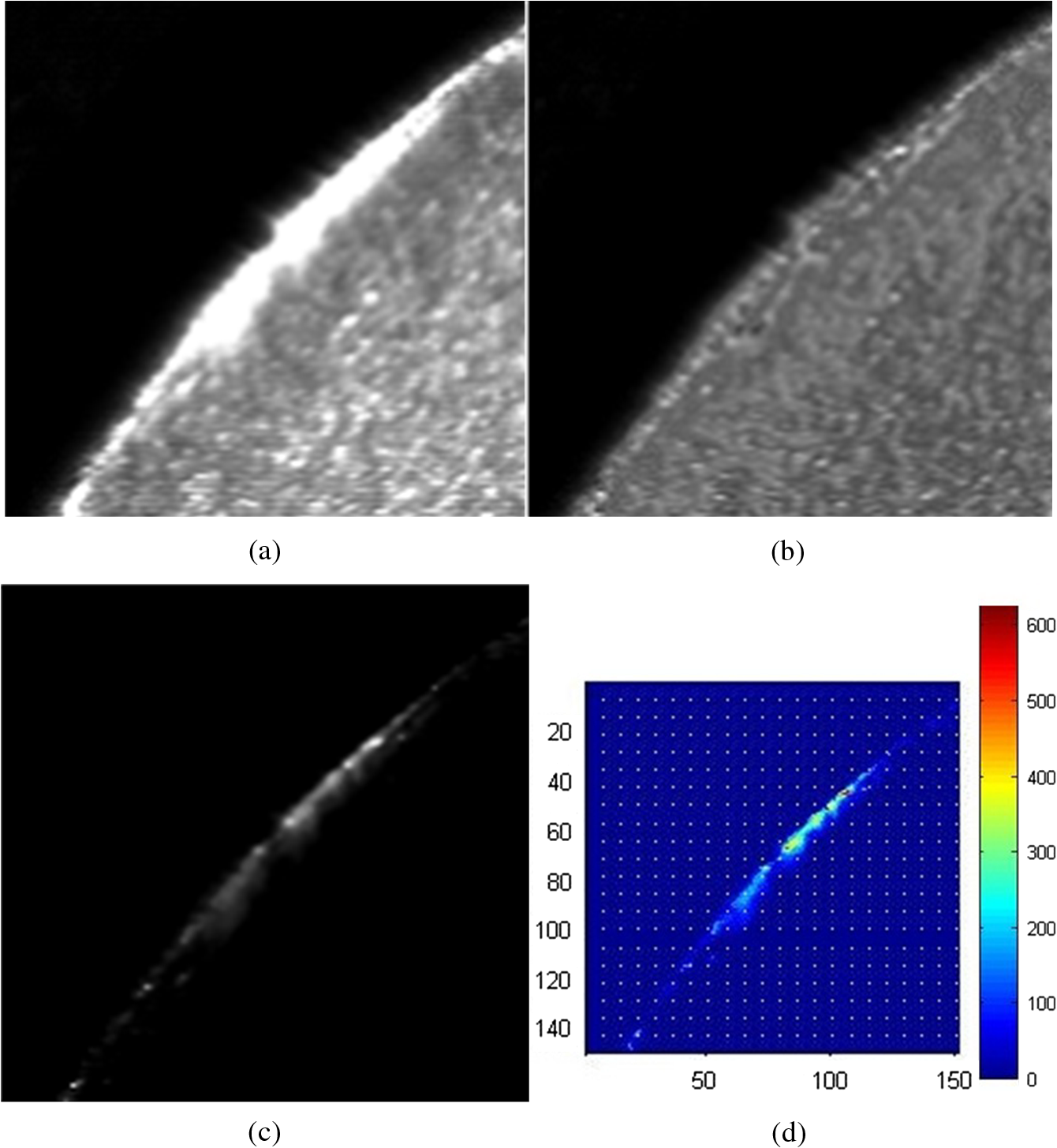 The other example is the removal of the parasitic image on a metal hemisphere, as shown in Fig. 7. Figure 7(a) shows the imaging scene of the metal hemisphere. The dashed box is the close-up region where the geometric and textural information of the metal hemisphere are covered by the highly reflective light. Figures 7(b), 7(c), and 7(d) are the close-up image, correction image, and parasitic image, respectively. Luminance estimation of the parasitic image as a by-product of the preceding strategy is shown in Fig. 7(e). Fig. 7The other example: (a) metal hemisphere, (b) a close-up of record image, (c) correction image, (d) parasitic image, and (e) intensity distribution of parasitic image. 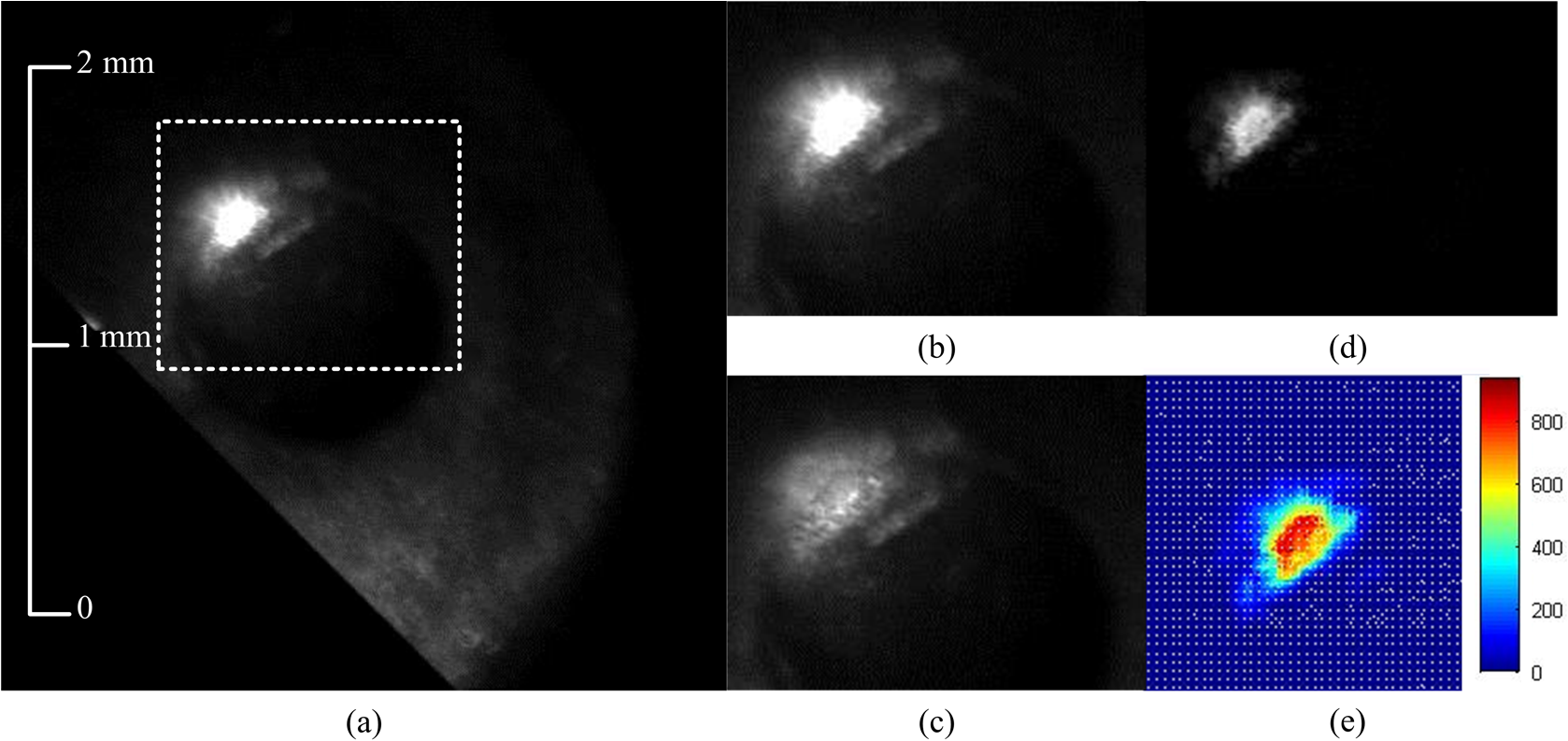 Experimental results show that the proposed approach successfully remove a parasitic image on metal surfaces of different shapes and sizes. Without multiexposure imaging or multi-illumination, we can recover almost the full resolution information by the SLM strategy. The DMD camera achieves its flexibility by using a programmable array of micromirrors. With our method, the highlight is reduced before image formation. As the SNR is improved, a high quality image is provided. A simple algorithm containing modulated area recognition, precise region mapping, and separation of parasitic image and correction image is effective to decrease time-consumption in host processor. 5.LimitationHowever, our method does suffer from limitations of precision and application. First, our method requires knowledge of the exact corresponding relationship between the CCD and DMD. Second, for achieving high accuracy mapping from the DMD to CCD, the depth of field of our setup should be limited to a small-scale range. Moreover, the high intensity of the central point source is not completely eliminated in our experiment. Third, our method can handle the highlight due to specular reflection, but the dynamic range of the DMD camera limits the removable parasitic image. The relationship between the DMD pixel digital value and reflectivity is given by where is the measured optical power; is optical power of incident light, and is the DMD level.Thus, we define the maximum removable parasitic image as where denotes the relational function between the CCD pixel digital value and the corresponding irradiance on CCD pixels; and is the CCD level.6.ConclusionA parasitic image created by strong highlights due to specular reflection covers useful information and reduces image contrast. Removing the parasitic image is a widespread requirement in science, medicine, and photography. In this article, a DMD camera composed of a DMD, CPU, and CCD is developed to achieve programmable imaging. We have developed a new method for removing the parasitic image from an optical system, using iterative modulation with a DMD camera to remove and estimate the parasitic image. Meanwhile, the method obtains the estimate of the parasitic image and provides a novel pathway to analyze and evaluate the parasitic image in optical system. As experimental results, the parasitic images on metal surfaces of different shapes and sizes are successfully removed. AcknowledgmentsThis work was supported by the National Natural Science Foundation of China (grant no. 51275350), Tianjin Natural Science Foundation (grant no. 12JCYBJC11000), and Doctoral Fund of Ministry of Education of China (grant no. 20110032110045). ReferencesS. A. Shafer,
“Using color to separate reflection components,”
Color Res. Appl., 10
(4), 210
–218
(1985). http://dx.doi.org/10.1002/(ISSN)1520-6378 CREADU 0361-2317 Google Scholar
A. ArtusiF. BanterleD. Chetverikov,
“A survey of specularity removal methods,”
Comput. Graph. Forum, 30
(8), 2208
–2230
(2011). http://dx.doi.org/10.1111/cgf.2011.30.issue-8 CGFODY 0167-7055 Google Scholar
R. BajcsyS. LeeA. Leonardis,
“Detection of diffuse and specular interface reflections and inter-reflections by color image segmentation,”
Int. J. Comput. Vision, 17
(3), 241
–272
(1996). http://dx.doi.org/10.1007/BF00128233 IJCVEQ 0920-5691 Google Scholar
H.-L. ShenQ.-Y. Cai,
“Simple and efficient method for specularity removal in an image,”
Appl. Opt., 48
(14), 2711
–2719
(2009). http://dx.doi.org/10.1364/AO.48.002711 APOPAI 0003-6935 Google Scholar
H.-L. ShenZ.-H. Zheng,
“Real-time highlight removal using intensity ratio,”
Appl. Opt., 52
(19), 4483
–4493
(2013). http://dx.doi.org/10.1364/AO.52.004483 APOPAI 0003-6935 Google Scholar
Q. YangS. WangN. Ahuja,
“Real-time specular highlight removal using bilateral filtering,”
in Proc. European Conf. on Computer Vision (ECCV),
87
–100
(2010). Google Scholar
Y. Y. SchechnerS. K. NayarP. N. Belhumeur,
“Multiplexing for optimal lighting,”
IEEE Trans. Pattern Anal. Mach. Intell., 29
(8), 1339
–1354
(2007). http://dx.doi.org/10.1109/TPAMI.2007.1151 ITPIDJ 0162-8828 Google Scholar
A. Agrawalet al.,
“Removing photography artifacts using gradient projection and flash-exposure sampling,”
in Proc. Acm Siggraph 2005 Conf., Acm Trans. Graphics,
828
–835
(2005). Google Scholar
A. Jaehyunet al.,
“A multi-exposure image fusion algorithm without ghost effect,”
in Proc. 2011 IEEE Int. Conf. on Acoustics, Speech and Signal Process. (ICASSP),
1565
–1568
(2011). Google Scholar
B. BitlisP. A. JanssonJ. P. Allebach,
“Parametric point spread function modeling and reduction of stray light effects in digital still cameras,”
Proc. SPIE, 6498 29
–31
(2007). http://dx.doi.org/10.1117/12.715101 PSISDG 0277-786X Google Scholar
C. C. LiebeL. ScherrR. Willson,
“Sun-induced veiling glare in dusty camera optics,”
Opt. Eng., 43
(2), 493
–499
(2004). http://dx.doi.org/10.1117/1.1635835 OPEGAR 0091-3286 Google Scholar
A. A. Goshtasby,
“Fusion of multi-exposure images,”
Image Vision Comput., 23
(6), 611
–618
(2005). http://dx.doi.org/10.1016/j.imavis.2005.02.004 IVCODK 0262-8856 Google Scholar
S. K. NayarV. BranzoiT. E. Boult,
“Programmable imaging: towards a flexible camera,”
Int. J. Comput. Vision, 70
(1), 7
–22
(2006). http://dx.doi.org/10.1007/s11263-005-3102-6 IJCVEQ 0920-5691 Google Scholar
S. RiM. FujigakiY. Morimoto,
“Single-shot three-dimensional shape measurement method using a digital micromirror device camera by fringe projection,”
Opt. Eng., 48
(10), 103605
(2009). http://dx.doi.org/10.1117/1.3250197 OPEGAR 0091-3286 Google Scholar
M. AnkitR. RameshT. Jack,
“Agile spectrum imaging: programmable wavelength modulation for cameras and projectors,”
Comput. Graph. Forum, 27
(2), 709
–717
(2008). http://dx.doi.org/10.1111/j.1467-8659.2008.01169.x CGFODY 0167-7055 Google Scholar
A. A. AdeyemiN. BarakatT. E. Darcie,
“Applications of digital micro-mirror devices to digital optical microscope dynamic range enhancement,”
Opt. Express, 17
(3), 1831
–1843
(2009). http://dx.doi.org/10.1364/OE.17.001831 OPEXFF 1094-4087 Google Scholar
S. Riet al.,
“Accurate pixel-to-pixel correspondence adjustment in a digital micromirror device camera by using the phase-shifting moire method,”
Appl. Opt., 45
(27), 6940
–6946
(2006). http://dx.doi.org/10.1364/AO.45.006940 APOPAI 0003-6935 Google Scholar
BiographyShou-Bo Zhao received his BS and MS degrees in optical engineering from Tianjin University in 2008 and 2011, respectively. He is a PhD candidate in the State Key Lab of Precision Measuring Technology and Instruments, Tianjin University. He is interested in optical metrology using image processing and computational camera development. |