|
|
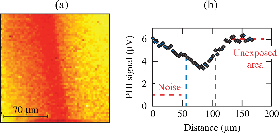
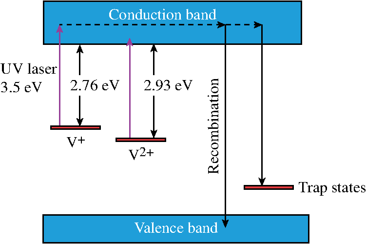
1.IntroductionHafnium oxide () is used in numerous applications as a high-index component in coatings for high-power lasers ranging from a near-infrared to near-ultraviolet (UV) light spectrum. It is also known that for the most frequently used film-pair combination of , is the material where nanosecond-pulse laser damage is initiated.1 In this context, reduction of absorption in this material is crucial to improving damage performance of the coatings used in mirrors and other laser components. Previous studies2 showed that near-UV absorption in thin films is generated by high-spatial-density (an average separation of 100 nm or less) nanoscale absorbers whose nature is attributed to the agglomeration of electronic defects. Electronic defects exist even in high-quality optical bulk materials, such as crystals and glasses. In thin films, additional absorbing states might exist because of the presence of interfaces and grain boundaries. There are very limited ways to influence the concentration of the absorbing states once the thin film is deposited. Thermal annealing3,4 is the process most frequently used as a research tool, but there are obvious practical limitations for optical parts used in large-scale lasers. Irradiation by pulsed laser radiation at fluences below damage threshold (also called laser conditioning) is another widely used method. In this work, we explore the possibility of using continuous-wave (cw) laser radiation with power densities in the range of to to anneal absorption in monolayer films in the near-UV spectral range. We also investigate the absorption-annealing impact on pulsed-laser damage behavior of monolayers subjected to irradiation by 351-nm, 0.9-ns pulses and 1053-nm, 600-fs pulses. 2.ExperimentalAn monolayer film with a 180-nm physical thickness (one wave at 351 nm) was -beam deposited on a fused-silica substrate on top of a 500-nm-thick silicon dioxide () film, isolating the film from the substrate defects introduced by the polishing process. The deposition rate was and the oxygen pressure was Torr. For monolayer absorption characterization, we used a photothermal heterodyne imaging (PHI) technique, utilizing pump and probe laser beams focused into a submicrometer spot on a sample having the same objective. Modulated pump-light absorption inside the sample produces a locally modulated refractive-index variation, which causes probe-light scattering amplified by far-field interference. Using the nanopositioning stage for the sample translation allows one to map absorption of the film sample with a spatial resolution better than 0.4 μm. Throughout this paper, the absorption will be quantified in terms of the PHI signal (in microvolts), which is proportional to the absorption cross-section. Calibration of absolute absorption values using photothermal techniques carries a high level of uncertainty and requires using a calibration standard with well-known thermal properties. In this work, we used 200-nm-thick titanium dioxide () film5 for calibration, with 49% transmission at 355 nm. These data provided an estimate (with 100% uncertainty) for the PHI sensitivity of 1 μV per 40 parts per million (ppm) absorptance, which is a ratio of absorbed power to incident power. film samples produced in different coating runs and used in this study showed some variation in initial 355-nm absorption, with the majority of samples characterized by absorptance. A detailed description of the PHI technique principle and the setup used in this work is given in Refs. 2 and 5. Near-UV cw laser–absorption annealing was studied using either a 351-nm, 1-W laser or a 355-nm, diode-pumped semiconductor laser that works as a pump laser for PHI and delivers up to 6 mW on the sample. The latter, after being focused into a [full width at half maximum (FWHM)] spot by a numerical-aperture objective, produced power densities of up to , and the former was focused into a 50-μm spot (), resulting in a power density. A sample exposure, in the case of a small laser spot (PHI pump laser), was accomplished by using two different methods. In the first method, the sample position and laser power were fixed and the sample was exposed for some period of time, typically up to 15 min. In this manner, several sample sites were irradiated at a different cw laser power. The second method consisted of raster scanning the sample with typical velocities of 1 to , producing different exposures by varying the sample velocity and laser power. To quantify the exposure effect at a particular location, another raster scan of the larger area, including the exposed area, was performed with a high sample velocity and low laser power to minimize additional energy deposition. In the case of a large laser spot ( laser), the sample was translated in one direction with a velocity, creating a 50-μm-wide, several-millimeters-long exposed area. Laser-damage testing of cw laser exposed and unexposed sample areas was performed in a 1-on-1 regime, using 351-nm, 0.9-ns pulses of a Nd:YLF diode-pumped laser6 and 1053-nm, 600-fs, best-compression pulses from a laser using the standard chirped pulse amplification scheme.7 Damage testing using 0.9-ns pulses was conducted in an ambient environment and testing with 600-fs pulses was performed in a vacuum to avoid self-focusing in air. The laser beam spot size () on the sample was 400 and 270 μm for 0.9-ns and 600-fs beams, respectively. Laser-damage morphology was investigated by means of atomic force microscopy (AFM). 3.Results and Discussion3.1.Absorption-Annealing EffectsFigure 1 shows the result of irradiating the film for 8 min at a fixed location using a 355-nm, 6-mW beam focused into a submicrometer spot (, power density). Figure 1(a) is a PHI scan of a film area centered around the location of the laser spot. A cross-sectional profile of the PHI signal [Fig. 1(b)] shows up to 70% reduction in absorption within the irradiated spot, which appeared to be permanent when confirmed by PHI scans performed after one week and then one month later. Next, absorption annealing was investigated as a function of laser power and exposure time. Figure 2(a) plots a normalized PHI signal’s dependence on exposure time for three different values of laser-beam power: 0.7, 3, and 6 mW. One can see that the main drop in signal takes place during the first minute and is then followed by a slow decline on an - to 15-min time scale. The initial signal drop becomes faster and deeper with increasing laser power. Nevertheless, the temporal behavior of the 6- and 3-mW curves shows that at long exposures, the signal can eventually be stabilized at the same level. It suggests that within some range of power densities, overall absorption reduction is proportional to both power density and exposure time or, in different terms, locally deposited energy. This notion is strongly supported by the data presented in Fig. 2(b), showing the PHI signal plotted as a function of energy dose (incident power–time product). One can see that the data for different laser powers merge together, thereby confirming that the deposited energy (which is proportional to the energy dose) is a defining factor for producing absorption annealing effect. Fig. 1(a) A photothermal heterodyne imaging (PHI) map of a film area. (b) The signal horizontal profile through the central spot irradiated by a 355-nm, 6-mW cw laser for 8 min.  Fig. 2(a) Temporal behavior of absorption as a function of cw laser power on sample. (b) Normalized PHI signal for different laser powers as a function of energy dose (incident energy–time product). 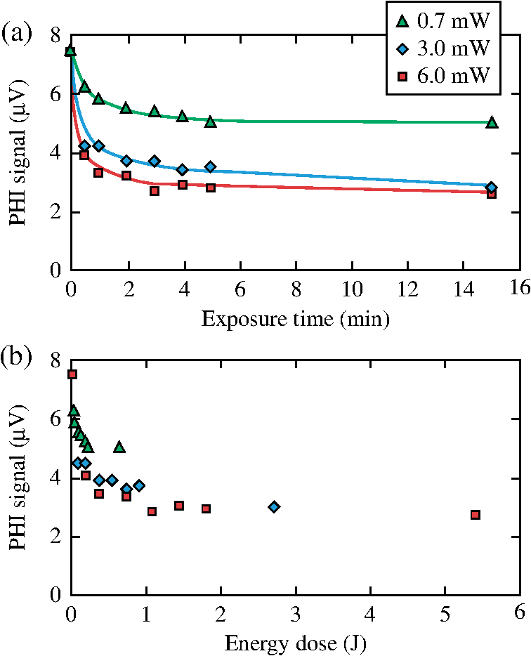 In an attempt to demonstrate the possibility of annealing absorption within a sample area larger than the laser spot, we performed square raster scans with linear dimensions of several tens of micrometers. Figure 3 shows corresponding PHI images, each obtained as a result of two scans. In the first image [Fig. 3(a)], the central part was initially scanned with a high laser power of 4.5 mW and a low scan velocity of to achieve the annealing effect. Subsequently, the larger square area (), with the same center coordinate, was imaged using a much lower laser power of 1.5 mW and a several-times-higher speed velocity, such that no, or very little, annealing effect was produced by the second scan. A cross-section horizontal signal profile revealed at least a 40% reduction in absorption within the initially scanned area. A similar procedure was used for the image shown in Fig. 3(b), with the only difference being that the central spot was exposed for an additional 8 min using a 6-mW laser power. In this case, the horizontal signal profile shows a 70% reduction in absorption in the central spot. From a practical point of view, it should be noted that because of the scan velocity and beam size limitations (the latter defines the maximum separation between two consecutive scan lines, or minimum number of lines per scan), raster scanning for annealing purposes is very time consuming. For example, it takes at least 2 h to complete a scan using a scan velocity. Fig. 3PHI maps resulting from 355-nm cw laser annealing by means of raster scanning with a low, sample velocity: (a) a area with the central part exposed using 4.5-mW laser power; (b) a area with the central part raster scan exposed, using 6 mW and, in addition, the central spot exposed for 8 min with 6-mW power; (c) and (d) horizontal signal profiles taken through the central part of (a) and (b) maps, respectively. 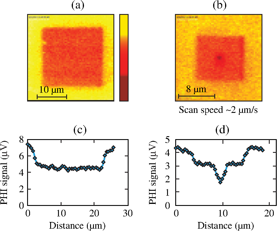 The question to be addressed is the possibility of scaling up the absorption-annealing process for films used in optical parts for laser applications. In this work, we explored the possibility of producing absorption annealing in a -scale area using a cw laser having a maximum 351-nm output power of 1 W. In this case, a laser beam having a power of was focused into a 50-μm-diameter () spot on the sample, which was slowly () linearly translated for a distance of 3.6 mm. Despite a much lower power maximum density of as compared to in the case of a small PHI pump laser spot, a much longer (at least ) exposure time allowed us to achieve an absorption reduction (see Fig. 4) in the film area of . In this exposure regime, the energy dose per unit of film area is comparable with an exposure using a small beam with a power of 0.7 mW (see Fig. 2). 3.2.Laser-Damage Performance of Annealed Films3.2.1.Nanosecond-pulse damageLaser-damage performance of thin films is usually strongly linked to the absorption properties of the film material and, therefore, can provide a true measure of absorption annealing. In this work, damage thresholds and damage morphology were investigated for cw laser–annealed film areas and then compared to the damage behavior of unexposed, as-produced film areas. As a starting point, we conducted AFM imaging of the cw laser–annealed film columnar structure, which was then compared to the columnar structure of the unexposed film. High-resolution () AFM images of these two areas (see Fig. 5) did not reveal any modification caused by the near-UV, cw laser exposure with power densities up to , implying that local heating of the material produced temperatures well below the melting point. Fig. 5Atomic force microscopy (AFM) images () of cw laser, unirradiated (a) and irradiated (b) film areas. 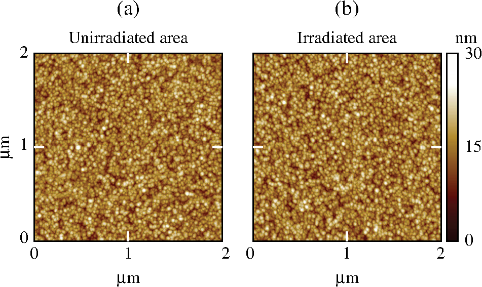 To evaluate the effect of absorption annealing on film-damage resistance, a series of cw laser–exposed areas were produced on a sample and then irradiated by a pulsed laser at fluences exceeding the damage threshold. Figure 6 depicts an optical micrograph of such a film area irradiated by a 351-nm, 0.9-ns pulse with a peak fluence ~30% above the threshold. A square-shaped unaffected area where cw-laser exposure was carried out is clearly visible inside the damaged zone. Laser-fluence estimates show an increase in damage threshold within the film area subjected to annealing, which unambiguously proves that absorption is reduced in cw laser–exposed film. Fig. 6An optical micrograph of an film site damaged by a 351-nm, 0.9-ns single pulse. Damage morphology clearly shows a damage-free, square area subjected to exposure by a 6-mW, 355-nm cw laser. 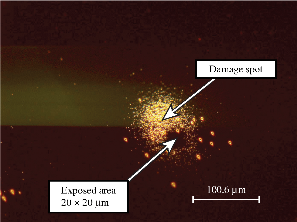 A high-resolution AFM map (see Fig. 7) of the sample site, shown earlier in Fig. 6, provides additional information of the impact of annealing on absorption sources in film material. Taking into account that damage morphology is represented by isolated craters, crater depth distribution provides a rough approximation for the localized absorber distribution within the sample material. The crater depth distribution was measured for the damage site area adjacent to the exposed area [Fig. 7(b)], which should provide a reasonable estimate of the initial absorber distribution within the exposed material. One can see that the crater depth does not exceed the 180-nm depth that equals the thickness of the layer. This result indicates that annealed absorption precursors are indeed located inside the film and not in the film or the substrate. Fig. 7(a) A AFM scan of a nanosecond-pulse damaged film site, including part of a cw laser–exposed area. (b) A higher-resolution, scan showing damage craters bordering an undamaged cw laser–irradiated area. (c) Crater-depth distribution confirming the location of absorption sources inside the 180-nm-thick film. 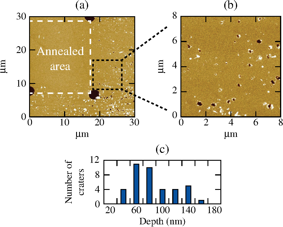 3.2.2.Short-pulse (600-fs) damagePrevious studies8 suggest that electronic defects might also play a role in short-pulse (picosecond, femtosecond) laser damage. In this context, the possible impact of the cw laser annealing of the absorption precursors on the short-pulse damage performance is of interest. Similar to the nanosecond-pulse study, near-UV, cw laser irradiation of a film was conducted utilizing both a small spot () of a PHI laser and a 50-μm spot of an laser. The results of the 1053-nm, 600-fs pulse damage testing of exposed (sites 1 and 2) and unexposed (sites 3 and 4) film areas are presented in Fig. 8, showing damage morphologies as recorded by an optical microscope. It is evident that the exposed sites show no damage at all while being irradiated by pulses with fluences above the unexposed film threshold of (compare sites 1 and 3) or show a smaller extent of damage (site 2 versus site 4) as compared to the unexposed sites. Moreover, as evidenced by the PHI image of damaged site 2 [see Fig. 8(b)], the damaging pulse has partially missed the exposed area, which, in the case of a better overlap, could show an even larger difference in the damage scale for sites 2 and 4. Fig. 8(a) Optical micrographs of 600-fs pulse-damage morphology. Sites 1 and 2: cw laser irradiated; sites 3 and 4: unirradiated. (b) PHI scan of site 2 showing relative positions of the cw laser–irradiated area and damaging-pulse imprint. 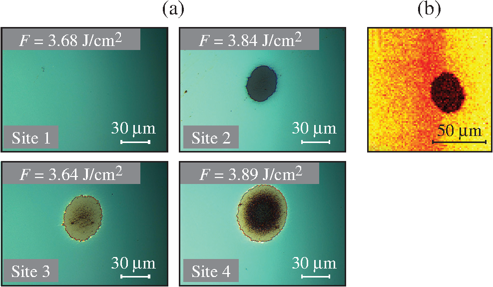 To summarize, near-UV, cw laser annealing improves the damage resistance of -beam–deposited films to pulsed laser radiation. 3.3.Absorption-Annealing MechanismsMechanisms of the near-UV, cw laser annealing of absorption in films and related improvements in pulsed laser-damage resistance may be explained if one considers electronic defects as a main source of absorption and damage initiation. Numerous types of defects can exist in bulk material with electronic energy levels located inside the bandgap9 and even more are expected to exist for films caused by the columnar film structure. As suggested earlier,2 in the case of near-UV nanosecond-pulse damage, some of these states—as single- and double-ionized oxygen vacancies [, , respectfully (see Fig. 9)]—are shallow enough that absorption of 351-nm photons (3.54 eV) can initiate transition of the electron into the conduction band. Further heating of these free electrons by the remaining laser pulse energy can promote electron avalanche formation and damage. The same defect energy levels might initiate multiphoton absorption and damage in the case of short, 600-fs pulses at 1053 nm. Assuming the validity of such a damage mechanism, the cw laser–induced absorption-annealing effect and linked increase in pulsed laser-damage resistance can be explained by depopulation of the absorbing states. The first possible scenario might involve cw laser–excited electron transition into the conduction band, where the electron spends time on the order of 10 ps (Ref. 8), followed by recombination with holes in the valence band or trapping into the deep defect states in the bandgap, as shown in Fig. 9. Modeling this scenario using kinetic equations may provide further clarification of the annealing mechanism. This type of study, as well as extending the investigation of cw laser annealing from monolayers to multilayer systems, should become the subject of future research. The second absorption-annealing scenario may be linked to the heating of the film material resulting from the absorption of UV-laser photons. Thermal annealing is widely used to improve the mechanical and optical performance of thin films, including laser-damage resistance in the near-UV, as was recently demonstrated10 for monolayer films at a 355-nm wavelength. In that work, the film temperature was increased by at least 100°C above room temperature in order to observe the absorption-annealing effect, with the maximum effect obtained at an annealing temperature of 300°C. To evaluate possible thermal effects in our study, the temperature distribution in the film was modeled with the assumption that all of the energy absorbed in the film is released in the form of heat. The energy deposition was considered homogeneous in the cylindrical film volume with a diameter equal to the FWHM diameter of the laser beam () and a height equal to a 180-nm film thickness. The geometry of the model is shown in Fig. 10(a). The cw laser intensity was fixed at (highest used in the experiment), and the energy deposited in the film was varied through variation of the film absorption in the range of 10 to 1000 ppm, with the upper absorption boundary (1000 ppm) being well above the film absorption estimated from photothermal measurements. Heat conduction was considered to be the only channel of energy dissipation, and temperature rise in the film was obtained by solving appropriate heat-conduction equations. where , , and are the density, heat capacity, and heat conductivity of the materials, respectively; is the temperature; and is the absorbed laser power per unit volume. The material parameters for modeling are listed in Table 1. No reliable data are available for the heat capacity and density values for and films; for that reason, their values were set equal to the bulk values. It should be noted here that these parameters in the cw laser regime affect only the time necessary to reach peak temperature but not the peak temperature value [as can be seen from Eq. (1) by setting the temperature derivative to zero]. A standard two-dimensional cylindrical (five-point spatial), time-explicit finite-difference scheme was used to discretize and solve the heat-conduction equation (see, e.g., chapter 8 of Ref. 11). The zero heat-flux boundary condition was applied at the film/air interface (), and a zero temperature- change boundary condition was applied at the other boundaries of the computational domain, which was chosen to be large enough to not affect the calculated temperature by more than 0.1°C. The results of the modeling presented in Fig. 10 show that at the highest chosen absorption level of 1000 ppm, the peak temperature rise does not exceed 14°C, which is not enough to produce the absorption-annealing effect. The two-dimensional temperature change distribution is shown in Fig. 10(a) along with its lineouts along the axis of symmetry () in Fig. 10(b) and along the axis () in Fig. 10(c). The time evolution of the maximum temperature rise, which is observed along the center of the laser beam at the interface, , after the laser is turned on at time , is shown in Fig. 10(d). It is worth noting that all these conditions lead to the highest-possible peak film temperature estimates. Adding energy dissipation channels (such as luminescence or structural transformations) would lead to lower peak temperatures. Consequently, one can conclude that depopulation of the absorbing states is not caused by a heat-induced structural matrix transformation.Fig. 10Peak temperature rise distribution in a thin-film sample: (a) modeling geometry and distribution in plane (); (b) lineout along axis (); (c) lineout along axis () ; and (d) time evolution of the maximum temperature rise. 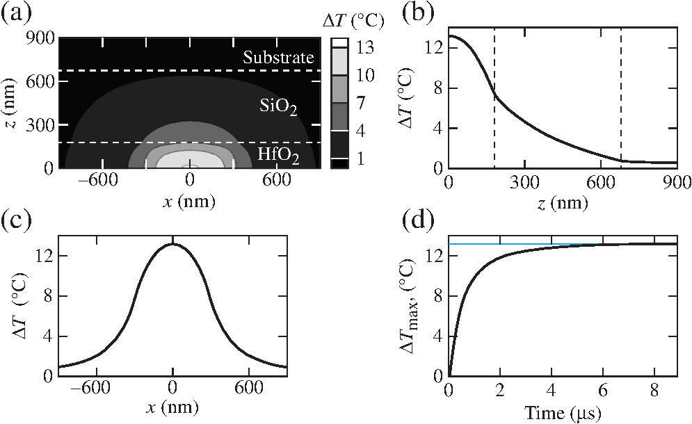 Table 1Parameters used to calculate the rise in hafnium oxide (HfO2) film temperature.
Finally, it should be noted that irradiation of thin films by cw lasers with power densities used in this work can produce different absorption-modification effects. For instance, in similar experimental conditions,12 irradiation of monolayer films using an 800-nm cw laser caused an increase in absorption that was also exposure-time dependent. Consequently, absorption-modification effects are thin-film material and cw laser wavelength specific. 4.ConclusionsIrradiation of e-beam–deposited monolayer films by near-UV, cw laser light with power densities of to produced significant modification of near-UV film absorption. As high as a 70% reduction in absorption was achieved in film areas subjected to exposure. The effect is permanent, as confirmed by repeated measurements over a several-month period. It is shown that absorption modification is achieved without any changes in the film columnar structure on a spatial scale of up to a few nanometers. This led to the conclusion that reduction of absorption is linked to the modification of the atomic film structure—in particular, to changes in the concentration of structural defects responsible for near-UV absorption. Investigation of 351-nm, nanosecond-pulse laser-damage behavior of monolayer films subjected to cw laser exposure showed a increase in damage thresholds and confirmed the reduction of absorption through annealing of absorbing defects residing inside the film. A 600-fs pulse irradiation also indicated an increase in laser-damage resistance of cw laser–exposed areas as compared to unexposed areas. This result suggests partial cw laser annealing of electronic defects participating in the multiphoton absorption process that initiates damage by 600-fs pulses. Future research will concentrate on further clarification of the annealing mechanism and will extend the study to multilayer systems. AcknowledgmentsThis material is based upon work supported by the Department of Energy National Nuclear Security Administration under Award Number DE-NA0001944, the University of Rochester, and the New York State Energy Research and Development Authority. The support of DOE does not constitute an endorsement by DOE of the views expressed in this article. ReferencesS. PapernovA. W. Schmid,
“Localized absorption effects during 351 nm, pulsed laser irradiation of dielectric multilayer thin films,”
J. Appl. Phys., 82
(11), 5422
–5432
(1997). http://dx.doi.org/10.1063/1.365570 JAPIAU 0021-8979 Google Scholar
S. Papernovet al.,
“Near-ultraviolet absorption and nanosecond-pulse-laser damage in monolayers studied in submicrometer-resolution photothermal heterodyne imaging and atomic force microscopy,”
J. Appl. Phys., 109
(11), 113106
(2011). http://dx.doi.org/10.1063/1.3594713 JAPIAU 0021-8979 Google Scholar
M. TilschV. ScheuerT. T. Tschudi,
“Effects of thermal annealing on ion-beam-sputtered and optical thin films,”
Proc. SPIE, 3133 163
–175
(1997). http://dx.doi.org/10.1117/12.279104 Google Scholar
G. Tianet al.,
“Microstructure and laser-induced damage threshold of coatings dependence on annealing temperature,”
Appl. Surf. Sci., 239
(2), 201
–208
(2005). http://dx.doi.org/10.1016/j.apsusc.2004.05.267 ASUSEE 0169-4332 Google Scholar
S. Berciaudet al.,
“Photothermal heterodyne imaging of individual metallic nanoparticles: theory versus experiment,”
Phys. Rev. B, 73
(4), 045424
(2006). http://dx.doi.org/10.1103/PhysRevB.73.045424 PRBMDO 0163-1829 Google Scholar
A. V. Okishevet al.,
“A highly energetic, multiwavelength, diode-pumped nanosecond laser system with flexible pulse-shaping capability,”
Proc. SPIE, 8599 85990Q
(2013). http://dx.doi.org/10.1117/12.2001687 PSISDG 0277-786X Google Scholar
H. P. Howardet al.,
“Improving the performance of high-laser-damage-threshold, multilayer dielectric pulse-compression gratings through low-temperature chemical cleaning,”
Appl. Opt., 52
(8), 1682
–1692
(2013). http://dx.doi.org/10.1364/AO.52.001682 APOPAI 0003-6935 Google Scholar
D. N. Nguyenet al.,
“Transient phenomena in the dielectric breakdown of optical films probed by ultrafast laser pulse pairs,”
Appl. Phys. Lett., 97
(19), 191909
(2010). http://dx.doi.org/10.1063/1.3511286 APPLAB 0003-6951 Google Scholar
A. S. Fosteret al.,
“Vacancy and interstitial defects in hafnia,”
Phys. Rev. B, 65
(17), 174117
(2002). http://dx.doi.org/10.1103/PhysRevB.65.174117 PRBMDO 0163-1829 Google Scholar
S. Kičaset al.,
“Characterization and application of mixtures produced by ion-beam sputtering technology,”
Proc. SPIE, 8885 888521
(2013). http://dx.doi.org/10.1117/12.2030308 PSISDG 0277-786X Google Scholar
R. D. RichtmyerK. W. Morton, Difference Methods for Initial-Value Problems, 2nd ed.Interscience, New York
(1967). Google Scholar
W. Rudolphet al.,
“Laser damage in dielectric films: what we know and what we don’t,”
Proc. SPIE, 8885 888516
(2013). http://dx.doi.org/10.1117/12.2030894 PSISDG 0277-786X Google Scholar
BiographySemyon Papernov graduated from Latvian University, Riga, Latvia, with BS and MS degrees in physics in 1972. In 1972, he joined the Latvian University, Spectroscopy Research Laboratory. His main activities included studies of energy transfer processes in alkali metal vapors by means of laser spectroscopy. In 1979, he received his PhD degree in physics from Latvian University. In 1988, he joined the Laboratory for Laser Energetics at the University of Rochester in Rochester, New York. His areas of scientific interests include optical materials for high-power lasers, laser-induced damage, thin solid films, and atomic force microscopy. Alexei Kozlov graduated from Leningrad Institute of Fine Mechanics and Optics in 1991, where he received his BS and MS degrees in optics. He has over 25 years of experience in high-power solid-state lasers, including chirped pulse amplification technique, optical phase conjugation and ultra-short optical pulse diagnostics. Since 2002 he has been at the Laboratory for Laser Energetics, University of Rochester, where his research interests are in the area of short-pulse laser damage testing. James Oliver is a scientist at the University of Rochester’s Laboratory for Laser Energetics, working primarily on design, process development, and production of hafnia/silica thin film coatings for high fluence applications including OMEGA, NIF, and other fusion-class lasers. He specializes in thin-film uniformity modeling, stresses, and system design for large-aperture coating deposition. He also teaches optical coating design at the Institute of Optics as well as at the institute’s annual thin film summer school program. Terrance J. Kessler is Optical and Imaging Sciences Group Leader at the University of Rochester’s Laboratory for Laser Energetics. He formed the Optics and Imaging Sciences group to support nuclear fusion research over the last 30 years. He has worked on the design and testing of high peak power lasers, laser coherence control, focal spot zooming, and the development of phase plates, and diffraction gratings. He currently serves as a secretary of the International Committee on Ultra-Intense Lasers. |