|
|
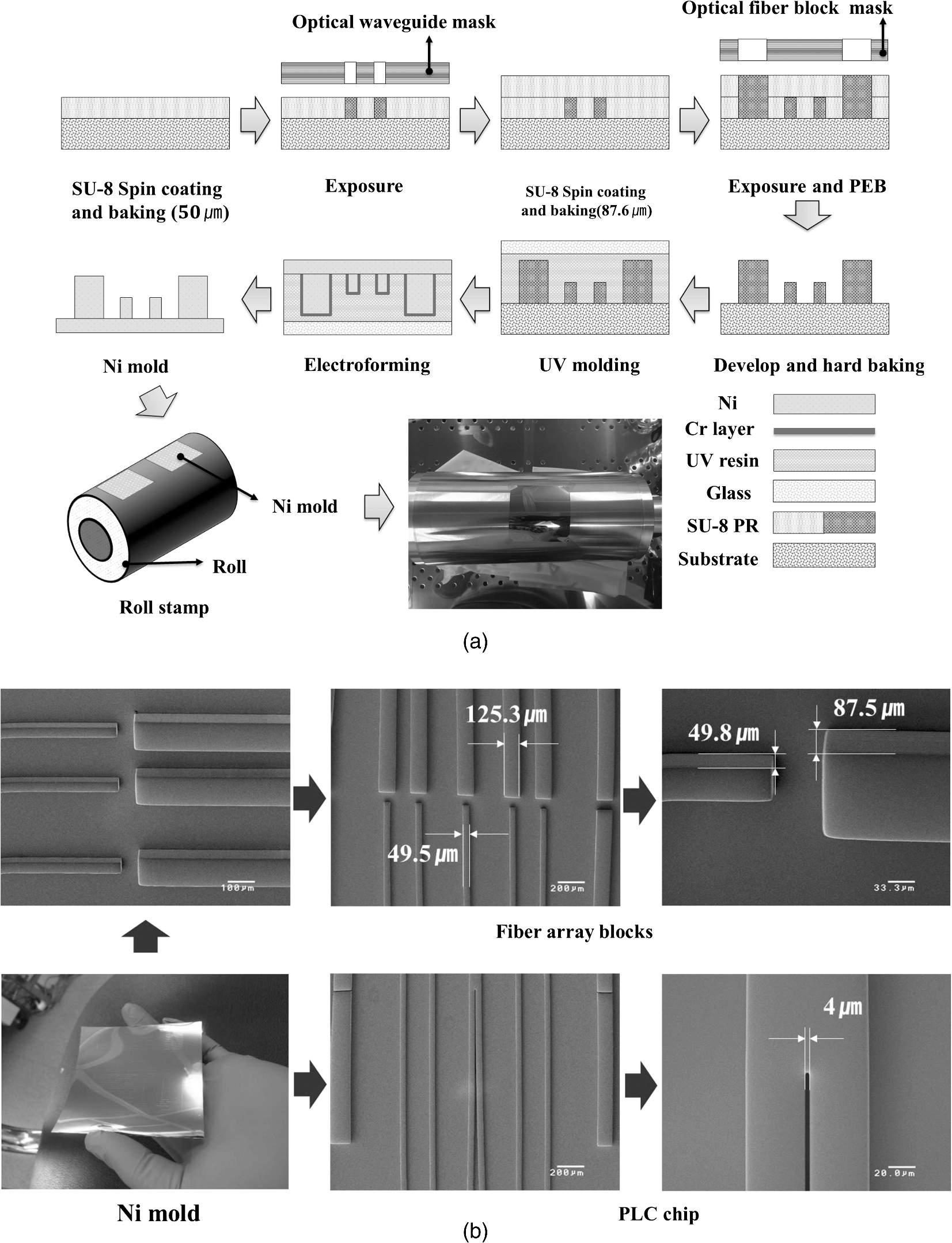
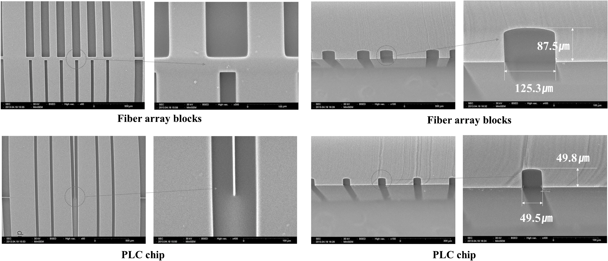
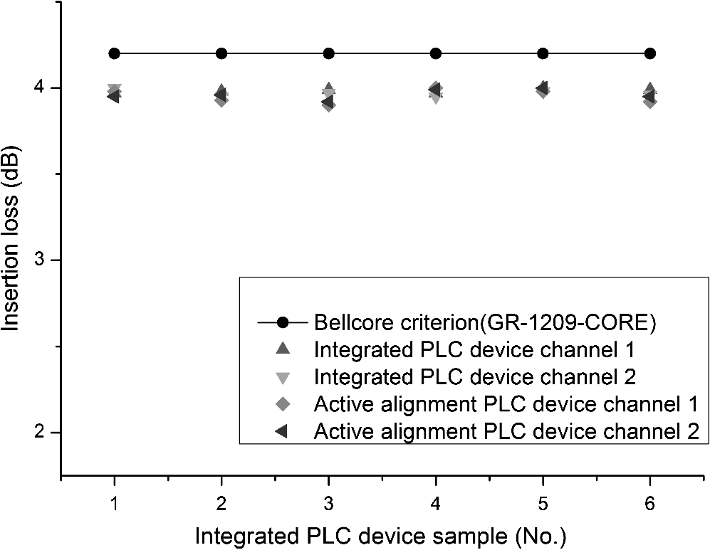
1.IntroductionNumerous studies have shown that planar lightwave circuit (PLC) devices have a low transmission loss and provide high speed data transmission of optical communications.1,2 Advances in polymeric PLC device technology have culminated in the development of devices with the same performance as silica PLC devices, indicating that polymeric PLC devices could replace silica PLC devices in the future.2,3 Compared to silica PLC devices, polymeric PLC devices are easier and quicker to produce, which benefits productivity.2,3 Unlike other waveguide materials, polymers can be directly deposited on any kind of flat or curved substrate.4 Tailored polymer materials also offer a high structural flexibility through different combinations of monomers, and accurate control of refractive indices and materials’ properties can be obtained.4 The low-temperature fabrication process of polymer waveguides offers the designer a large degree of freedom. Furthermore, polymeric materials permit the mass production of low-cost high-port-count photonic circuits in parallel on planar substrates, as well as providing the possibility for a much higher degree of ruggedness.4,5 Polymeric PLC devices can be mass produced using a simple process such as continuous roll-to-roll (R2R) imprinting to reduce costs.6,7 R2R imprinting uses a flexible substrate for continuity and forms the shape of the device using a roll stamp.7 The structure fabricated using R2R imprinting is then connected with an optical fiber to form the polymeric PLC device. Precision of the optical interconnection and bonding are essential elements for ensuring a low coupling loss and high-efficiency devices.1,6 Conventionally, fiber array blocks are used to align the optical fiber, which is then interconnected to the PLC chip. The fiber array blocks and PLC chip are typically fabricated separately, and high-precision alignment is necessary for bonding the PLC chip core and fiber core6 by curing an epoxy resin using ultraviolet (UV) light. To stabilize the bonding, the PLC-chip-fiber-block interface must be coupled to a certain degree, and deformation caused by shrinkage should be controlled during the UV hardening to minimize misalignment.3,8 However, because the R2R process uses a flexible substrate, shrinkage of the polymeric PLC chip area is likely to occur and core alignment problems arise, thus increasing the coupling loss in the optical interconnection. Moreover, thin flexible substrates may result in adhesion problems in the bonding area. These problems suggest that a new optical interconnection method may be needed. Here, we propose an integrated structure combining chip and fiber array blocks for the optical interconnection of polymeric PLC devices fabricated using R2R imprinting. The characteristics and effectiveness of the design are discussed. 2.Integrated Optical Interconnection DesignThe optical interconnection in the proposed integrated structure was designed to control the coupling loss generated by the misalignment of the polymeric PLC chip and fiber array blocks. The design was also optimized to facilitate R2R imprinting. The misalignment of the chip and fiber array blocks includes contributions from lateral offsets () in the -, -, and -directions, endface separation () of the PLC chip and optical fiber, and angular misalignment () of the PLC chip [Fig. 1(a)]. The alignment has a direct effect on the performance of the PLC device. Fig. 1(a) Parameters describing the coupling loss between the planar lightwave circuit (PLC) device chip and optical fiber. (b) Design of the integrated optical interconnection for the polymeric PLC device. 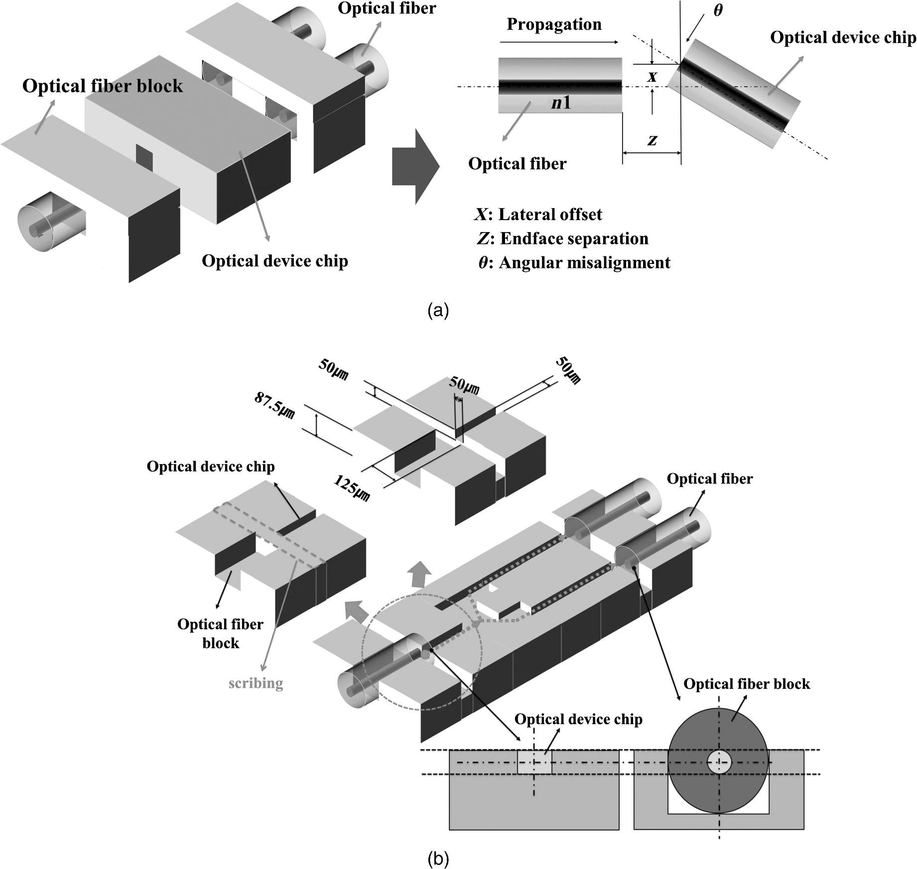 The integrated structure was designed so that the polymeric PLC chip and fiber array blocks were fabricated on the same substrate, as shown in Fig. 1(b), to solve the alignment and the bonding problems. The structure has a minimized extrinsic error and thus a reduced coupling loss. The centers of both the PLC core and the fiber core were positioned along the same axis for optical interconnection of the multimode optical splitter and multimode fiber; alignment was simply achieved with the insertion of the fiber. The fiber array blocks were wide and thick, whereas the PLC chip was wide and thick. A scribing process was used for the PLC chip and fiber contact surfaces. The integrated structure also includes a semiembedded fiber whose fiber axis was below the top surface of the substrate to ensure alignment with the PLC chip. The semiembedded fiber minimizes defects introduced from incomplete filling due to the short rolling time of the roll stamp and fast processing speed of the R2R imprinting. 3.Fabrication of the Roll Stamp and Integrated StructureFigure 2(a) shows the roll stamp used in the R2R imprinting process to fabricate the integrated structure. Since the widths and thicknesses of the PLC chip and fiber array blocks were different, the structure was fabricated using a multiple exposure patterning process with an SU-8 (Microchem Co., Newton, Massachusetts; SU-8 2075, 2025) negative photoresist (PR). The first spin coating and exposure process was executed using SU-8 2025 to fabricate the PLC chip, followed by another spin coating and exposure process to fabricate the fiber block. A -thick layer of SU-8 2075 was spin coated on the structure at 4500 rpm, and then a -thick layer of SU-8 2025 was spin coated at 2800 rpm to obtain a final PR thickness of . After the second exposure, the integrated interconnection structure was fabricated by developing, UV molding, and electroforming, which yielded the final embossed Ni stamp. The fabricated Ni stamp [Fig. 2(b)] was then attached to the roll cylinder for the R2R imprint. The fabricated PLC chip was wide and thick, and the final fiber array blocks were wide and thick. The dimensions of the fabricated structure were accurate to within 1% of those of the designed structure. 4.Effects of R2R Imprint Parameters on the Fabrication of the Integrated StructureBecause of the short forming speed and small area that is pressed in the R2R imprinting, defects in the integrated structure are more likely to appear in the height rather than the width.9,10 Therefore, the height characteristics for various roll pressures and web speeds, which are direct variables of the depth formation accuracy, were studied (Fig. 3); the other variables remained fixed during the tests. We see that process conditions for the precise formation of the PLC chip and fiber array blocks, which have different depths, can be determined. Fig. 3Influence of (a) roller pressure and (b) web speed on the height of the imprinted integrated structure (other processing parameters were fixed during each test trial). 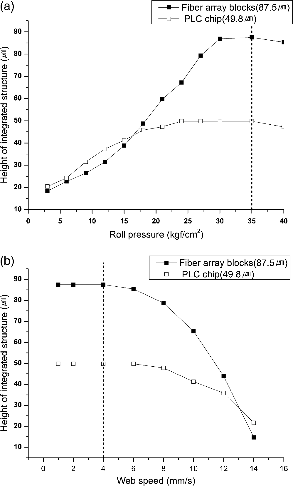 Figure 3(a) reveals that the roll-pressure formation condition was . When the roll pressure was higher than the formation condition, the height of the integrated structure decreased because there was an excess of polymeric resin. Figure 3(b) shows that if the web speed is too high, then the filling is incomplete because the polymeric resin and the roll stamp are pressed onto the film substrate for a short time. The height starts to decrease for web speeds greater than , so this was selected as the formation condition. Although a reduction in the web speed improves the accuracy of the pattern formation, longer processing times are needed. Figure 4 shows scanning electron microscope images of the integrated structure fabricated at the optimal process condition of a roll pressure and web speed. 5.Results and DiscussionAn integrated polymeric PLC device was fabricated by core filling the pattern fabricated with the R2R process and by inserting a fiber. A lamination process was used for the core resin filling and top cladding, and the fiber and PLC chip were then interconnected through the scribing process. To avoid overfilling in the fiber insertion zone of the core of PLC chip, the fiber array block patterns were connected. Figure 5(a) shows the steps involved in the optical interconnection process, and Fig. 5(b) shows the fiber bonding zone and cross section of the PLC chip of the fabricated integrated polymeric PLC device. Fig. 5(a) Steps in the manufacture of the PLC chip and (b) cross-sectional images of the fabricated PLC chip. 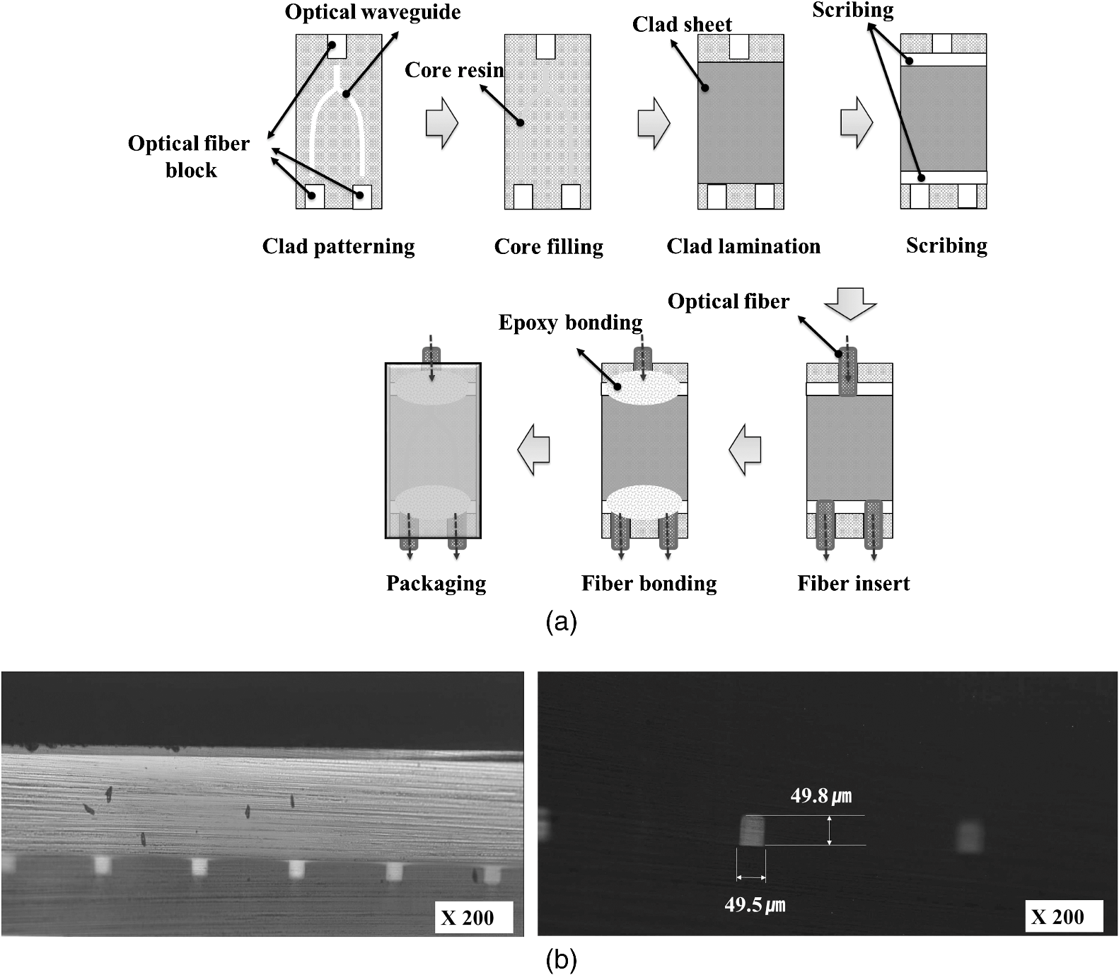 Figure 6 shows the insertion loss of the proposed integrated polymeric PLC device. In the case of conventional active alignment, the insertion loss was around 3.8 dB, and the uniformity of the optical splitter was less than or equal to 0.1 dB. For the alignment of the proposed structure, the insertion loss was around 3.9 dB, but the uniformity of the optical splitter was the same (0.1 dB or less). The insertion loss and the uniformity of a optical splitter device must satisfy the Bellcore criterion (GR-1209-CORE), i.e., an insertion loss of 4.2 dB and an optical uniformity of 0.6 dB. The proposed structure satisfies the criterion and can thus be used for practical optical interconnection. 6.ConclusionWe have developed an integrated structure to minimize the coupling loss generated by misalignment between the PLC chip and the fiber array blocks in creating an optical interconnection. The integrated structure was fabricated using R2R imprinting, and the central axes of the fiber array blocks and the PLC chip were aligned in all three spatial directions on the same substrate by the insertion of a fiber. The processing conditions for R2R imprinting were optimized, and the fabricated optical splitter device had an insertion loss of 3.9 dB and an optical uniformity of 0.1 dB. The proposed integrated optical interconnection structure does not require special alignment equipment and can be applied to practical PLC devices. AcknowledgmentsThis research was financially supported by the Ministry of Knowledge Economy (MKE), the Korea Institute for Advancement of Technology (KIAT), and the Dongnam Leading Industry Office through the Leading Industry Development for Economic Region. This work was supported by the Materials and Components Technology Development Program (10043786; Development of multifunctional nanopatterned polarizer film for display applications) funded by the Ministry of Trade, Industry and Energy (MI, Republic of Korea). ReferencesJ. H. Ryuet al.,
“Simple fabrication of a double-layer multi-channel optical waveguide using passive alignment,”
Opt. Express, 19
(2), 1183
–1190
(2011). http://dx.doi.org/10.1364/OE.19.001183 OPEXFF 1094-4087 Google Scholar
I.-B. SohnM.-S. LeeJ.-Y. Chung,
“Fabrication of optical splitter and passive alignment technique with a femtosecond laser,”
IEEE Photonics Technol. Lett., 17
(11), 2349
–2351
(2005). http://dx.doi.org/10.1109/LPT.2005.858101 IPTLEL 1041-1135 Google Scholar
J. H. Ryuet al.,
“Imprinted optical device and its reliability,”
Curr. Appl. Phys., 9
(2), e7e11
(2009). http://dx.doi.org/10.1016/j.cap.2008.12.022 1567-1739 Google Scholar
W. H. Wonget al.,
“Polymer devices for photonic applications,”
J. Cryst. Growth, 288
(1), 100
–104
(2006). http://dx.doi.org/10.1016/j.jcrysgro.2005.12.017 JCRGAE 0022-0248 Google Scholar
J. T. KimK. B. YoonC.-G. Choi,
“Passive alignment method of polymer PLC devices by using a hot embossing technique,”
IEEE Photonics Technol. Lett., 16
(7), 1664
–1666
(2004). http://dx.doi.org/10.1109/LPT.2004.828355 IPTLEL 1041-1135 Google Scholar
J. H. Ryuet al.,
“Optical interconnection for a polymeric PLC device using simple positional alignment,”
Opt. Express, 19
(9), 8571
–8579
(2011). http://dx.doi.org/10.1364/OE.19.008571 OPEXFF 1094-4087 Google Scholar
S. J. LiuC. T. Liao,
“Fast fabrication of nano-structured anti-reflection layers for enhancement of solar cells performance using plasma sputtering and infrared assisted roller embossing techniques,”
Opt. Express, 20
(5), 5143
–5150
(2012). http://dx.doi.org/10.1364/OE.20.005143 OPEXFF 1094-4087 Google Scholar
D. W. Kimet al.,
“Fabrication of thermally stable and cost-effective polymeric waveguide for optical printed-circuit board,”
Opt. Express, 16
(21), 16798
–16805
(2008). http://dx.doi.org/10.1364/OE.16.016798 OPEXFF 1094-4087 Google Scholar
L. P. Yeoet al.,
“Micro-fabrication of polymeric devices using hot roller embossing,”
Microelectronic. Eng., 86
(4–6), 933
–936
(2009). http://dx.doi.org/10.1016/j.mee.2008.12.021 MIENEF 0167-9317 Google Scholar
C. N. HuH. T. HsiehG. D. J. Su,
“Fabrication of microlens arrays by a rolling process with soft polydimethylsiloxane molds,”
J. Micromech. Microeng., 21
(6), 065013
(2011). http://dx.doi.org/10.1088/0960-1317/21/6/065013 JMMIEZ 0960-1317 Google Scholar
BiographySang Uk Cho is currently working toward his PhD degree at Pusan National University. His research interests are roll-to-roll lithography, nanoimprint lithography, and optical devices. Ho Ju Kang received his MS degree from Pusan University in 2012. He is currently working toward his PhD degree at Pusan National University. His research interests are light-emitting diodes, organic light-emitting diodes, and lithography. Sunghwan Chang received his BS degree from Pohang University of Science and Technology in 2001 and his MS and PhD degrees from the Korea Advanced Institute of Science and Technology (KAIST) in 2003 and 2009, respectively. He currently holds positions at KIMM, the University of Science and Technology, and KAIST. His research interest is in developing simple, cheap, and innovative fabrication methods for nanomicrohybrid structures and nanobioapplications. Doo Sun Choi received his BS and MS degrees from Yeungnam University in 1985 and 1989, respectively, and his PhD degree from Yonsei in 2002. He has been at KIMM since September 1990 and currently heads a laboratory in the Department of Nano Manufacturing Technology. His present research interests include manufacturing process and technology for nano- and microhybrid patterns. Chang-Seok Kim received his BS degree from the Korea Advanced Institute of Science and Technology in 1996, his MS degree from the Gwangju Institute of Science and Technology in 1999, and his PhD degree from Johns Hopkins University in 2004. Since 2009, he has been an associate professor in the Department of Cogno-Mechatronics Engineering, Pusan National University. His research interests include development of novel fiber laser systems and their applications in biomedicine, telecommunications, and sensors. Myung Yung Jeong received his BS and MS degrees from Pusan National University in 1982 and 1984, respectively, and his PhD degree from the Korea Advanced Institute of Science and Technology in 2000. Since September 1983, he has worked at the Electronics and Telecommunications Research Institute. He is currently a professor in the Department of Cogno-Mechatronics Engineering, Pusan National University. His present research interests include imprinted optical devices, nanophotonics, optical interconnection, and optical components for in-vehicle networks. |