|
|
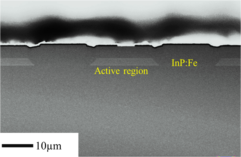
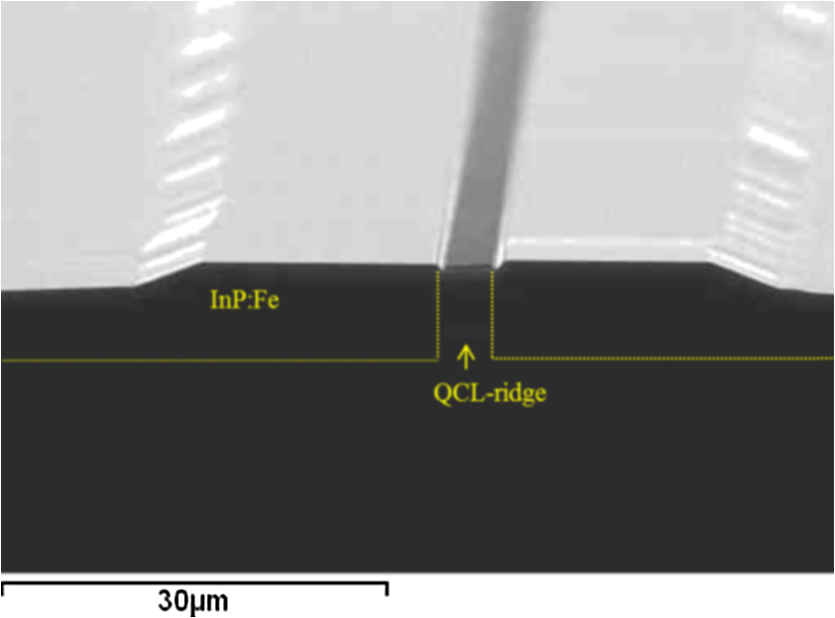
1.IntroductionQuantum cascade lasers (QCL) emerging from the physical concepts of the amplification of electromagnetic waves in a semiconductor superlattice1 was first demonstrated by Faist and coworkers.2 It is now shown to cover a wide range of the electromagnetic spectrum from near-infrared to midterahertz.3,4 In virtue of such a wide coverage of wavelengths, QCLs have become attractive sources for spectroscopy, medical and biosensing, remote gas sensing, free-space communication, and applications in defense security countermeasures. Several of these application areas necessitate high power, good beam quality, efficient thermal dissipation, and high wall plug efficiency (WPE). Together with the optimal basic design, buried heterostructure QCL (BH-QCL) with semi-insulating regrowth offers a unique possibility to achieve an effective thermal dissipation and lateral single mode, which help to achieve the above expected performance. The first BH-QCL was realized by Beck et al. using unintentionally doped InP (Ref. 5) by molecular beam epitaxy (MBE). Several advantages of BH-QCL have also been enumerated by Beck et al.6 in their report of the first continuous wave (CW) operation of BH-QCL. Later, several investigators have demonstrated BH-QCLs by metal organic vapor phase epitaxy (MOVPE)7–9 and gas source MBE (Refs. 10 and 11) using semi-insulating Fe-doped InP (SI-InP:Fe), which is already an established method in the fabrication of telecom lasers. So far, hydride vapor phase epitaxy (HVPE) has not been used to fabricate BH-QCLs using SI-InP:Fe. In view of the near-equilibrium nature of the process of HVPE, a small change in supersaturation (or a small change of chemical potentials between the reactants and the products) results in a high growth rate. Hence, its growth rate is often one order of magnitude higher than that of the nonequilibrium processes such as MOVPE and MBE. In addition, its planarization ability, total selectivity during the growth on patterned (planar or nonplanar) surfaces, nonappearance of “rabbit ears”12 near the ridge (or mesa) edge, flexibility in growing around [110] and [] oriented ridges, both with or without mask overhang, and insensitivity to the profile of the etched ridge are its unique features.13 However, due to the same fundamental near-equilibrium nature of HVPE, it can hardly grow quantum structures with monolayer control as MOVPE and MBE can do, since a small perturbation in the supersaturation causes a large variation in thickness. An added and attractive feature of an equilibrium process is the capability of achieving in situ ridge etching and immediate regrowth, which has been demonstrated for telecom lasers.14 When the Al-containing layers are etched (as ridge or mesa) and exposed to the atmosphere (prior to regrowth), the risk of immediate oxidation can cause problems for regrowth. To circumvent this problem, a combination of ex situ and in situ etching and immediate regrowth can be employed as has been demonstrated in the realization of BH-vertical cavity surface emitting lasers with GaAs/AlAs Bragg mirrors.15 This is also applicable for realizing BH-QCLs that contain Al-containing layers in the active region. All of these are attractive, especially for the realization of BH-QCL lasers in a short time. Maintenance of the QCL ridges at the regrowth temperatures for a longer time to realize BH-QCL can cause severe inter well-barrier mixing as has been demonstrated with telecom lasers,16 leading to the loss of the originally designed laser characteristics. Hetero-cascade17,18 and multistack QCLs,19,20 with several different active regions stacked on top of each other, are used to obtain a broad composite gain or increase peak power output. Such structures have thick etch ridges, which put a severe demand on carrying out regrowth around very deeply etched () ridges in a short time. In addition, in the future, advanced photonic integration with QCLs with arrayed waveguide gratings and detectors will be emerging and we foresee that HVPE is very useful as it has been demonstrated vital for the realization of photonic integrated chips.21,22 As QCLs have reached the commercialization stage, it is imperative that the fabrication processes are also less time consuming, flexible, and cost-effective. In this article, we demonstrate the realization of BH-QCL for the first time by HVPE. We focus mainly on the regrowth aspects revealing its rapidity and flexibility in achieving well planarized BH-QCL. Chips on an AlN submount were characterized and these exhibit an output power of 1.5 to 2.5 W under continuous wave operation and at 20°C with a WPE of 8 to 9%. The AlN submount was chosen instead of a high thermal conductivity submount. This leads to more reproducible results, but at the expense of lower performances. 2.ExperimentalAll the regrowth was conducted in a single step. This means that the regrowth around the whole QCL structure, including top and bottom cladding layers, was conducted in one step. Afterward, one can process the structure further with metal contacting without any further regrowth. In many of the earlier regrowth works, especially in telecom lasers, it is customary that a semi-insulating regrowth is done around only a partial structure ending with an active layer with/without part of the cladding layer and afterward, the mask is removed and one more regrowth of cladding layer is done, so these involve a two-step regrowth. Such a structure has sometimes been called a flat-buried heterostructure. Of course, although both single-step and double-step regrowth may have certain advantages,23 our work with single-step regrowth reduces to one processing step and the results presented are based on single-step regrowth only. Two basic sets of quantum cascade lasers, grown by MBE, were taken into consideration. The first set emitting at with a bound-to-continuum design reproduced from Blaser et al.24 was primarily meant to test the regrowth feasibility in terms of planarization with wet-etched ridges with overhang. The ridges were defined by photolithography using a 500-nm-thick hard mask, opened using a plasma etch. The ridges themselves were etched in a solution of . For an etch depth of 8 to , the expected undercut is on each side. After processing, these lasers were mounted epi-up and characterized. The 2-mm-long chips contained ridges with a width ranging from 17 to . The second set contained lasers emitting at . The structure of the laser is as described in Ref. 25. These were processed so as to analyze the advantage of BH design in terms of thermal dissipation. Identical lasers were processed in two configurations, one in ridge-only variation, where the ridges were covered with , and the other with a BH variation involving semi-insulating regrowth. These are shown schematically in Fig. 1. Fig. 1Schematic description of (a) ridge-only and (b) buried heterostructure (BH) quantum cascade lasers (QCLs) from the second batch. 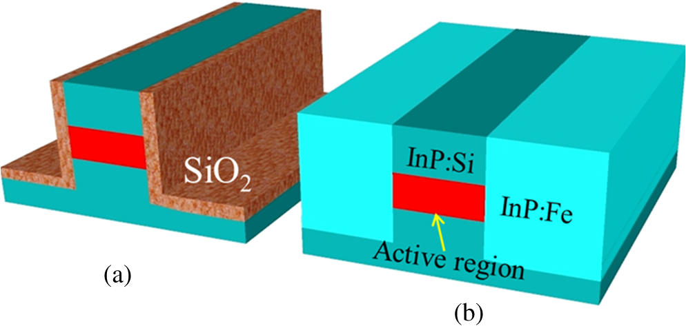 The ridges of width 4 to were etched with inductively coupled plasma etching using as the mask. The ridge-only variation was further processed with a coating of as shown in Fig. 1(a). The BH structure was realized in a low-pressure HVPE reactor with semi-insulating InP:Fe regrowth at a growth temperature of 600°C. The reactor pressure was maintained at 20 mbar and total gas flow in the reactor was 900 sccm. The V to III ratio, , was 10. The growth time was adjusted depending on the etched ridge depth, in all experiments. The size of the samples loaded into the reactor each time varied from one to four quarters of a 2-in. wafer to one full 2-in. wafer. The processed lasers were cleaved, high reflective (HR)-coated, and characterized. HR coating is done by ion-assisted deposition in a DENTON facility of followed by a Ti/Au layer, which provides the optical feedback. Standard characterization is made on a temperature-stabilized bench with a Peltier cooler. The mounting was done epi-side down on an AlN submount using gold tin soldering. The second contact is taken from the back side since the substrate is conductive and wire bonded. 3.Results and Discussions3.1.5.5-μm QCLIn case of the first set of samples, regrowth of InP:Fe was conducted on a wet-etched ridge with a depth of and a mask overhang of on each side. A complete planarization was obtained with only 13 min of regrowth time. The regrowth profile is shown in Fig. 2. The 3-mm-long chips with ridges after regrowth were mounted epi-side up on a copper heat-sink temperature controlled at 20°C with a Peltier cooler. These were operated in pulsed mode at 5% duty cycle and 20 kHz repetition rate. Figure 3 is the I-V-L curve of these chips. Fig. 3I-V-L curve of BH-QCL emitting at measured at 20°C under pulsed conditions (duty cycle , repetition rate ). 3-mm-long chips with ridges were mounted epi-side up on copper heat sink. 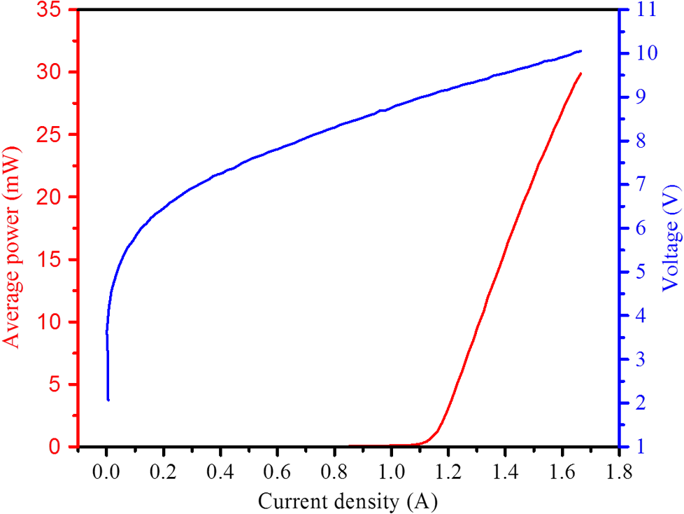 We observe that the regrown interface is seamless and the planarization ability is remarkable. The I-V curves measured under pulsed conditions with a duty cycle up to 20% indicate that there is no leakage. The reason why continuous wave operation is not reached may be attributed to the too large width of the ridges as well as high doping in the structure as can be inferred from the maximum current density of . 3.2.4.7-μm QCLThe cross-sectional view of the BH-QCL fabricated from an etched ridge is shown in Fig. 4. We also conducted, in a separate experiment, regrowth around a -striped QCL (Ref. 26) (not treated here), shown in Fig. 5. It is clearly seen that our regrowth process with a clean regrown interface yields good planarization without any rabbit ear formation. We would like to point out that the realization of total planarization across the entire sample depends upon the ridge etch depths and the distance between them, but is largely insensitive to the sample size. When the etched ridges are deep and the distances between them are large, sufficient planarization near the mesa to enable adequate metal contact on the ridge in the subsequent process can be achieved in a relatively short time, e.g., 20 min as in the case of regrowth in Fig. 4. As we have conducted numerous experiments with varying depths of etched ridges, it is possible to summarize the InP:Fe regrowth time as a function of etched ridge depth, as shown in Fig. 6. The data points in Fig. 6 are a collection from several regrowth runs on etched QCL ridges of different widths, separations, and even basic structures. Even though it may suffer from a certain consistency, we believe that these are qualitatively informative for the rapidity of the regrowth process. It is clear from this figure that the regrowth of InP:Fe around a ridge can be done in . This quick regrowth time is particularly interesting to minimize the risk for the unwanted intermixing of well and barrier as described earlier by Glew et al. for telecom lasers.16 These authors investigated the blue shift caused by the intermixing of wells and barriers at temperatures ranging from 550 to 750°C for varying durations of up to 120 min. They concluded that the blue shift of the investigated telecom laser is a power function of time and an exponential function of temperature. Although no similar annealing results on QCLs are available in the literature, intermixing phenomena in QCLs are likely to result in changes in the designed operation wavelength and in performance. The I-V-L curves for three BH-QCLs resulting from and ridge are shown in Fig. 7. The figure shows reproducible behaviors from laser to laser. Lasers of the same dimensions were studied in this investigation. A parametric study of the laser performances versus the geometrical parameters of the laser could give more insight into the performances of the processed wafer for other dimensions. However, in this study, it was not feasible due to the amount of material that was processed. In the new study, we plan to perform such an analysis. Figure 8 depicts the far-field pattern of three lasers of 6, 12, and ridge width and operating in a continuous wave at room temperature with 1.5, 2, and 2.1 A current levels, respectively. The far-field pattern for all lasers maintain a single Gaussian line profile, indicating a spatially monomode () behavior. Fig. 7I-V-L curves under CW operation at 20°C of three BH-QCLs of ridge width . The etched depth was . 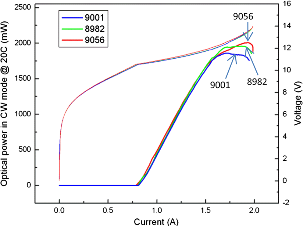 Fig. 8Far-field pattern of the buried lasers with different ridge widths of 6 to showing behavior. The main frame is the far field with respect to the slow axis and the inset is the far field with respect to the fast axis. Only one far field is shown in the fast axis since it is not influenced by the ridge width. 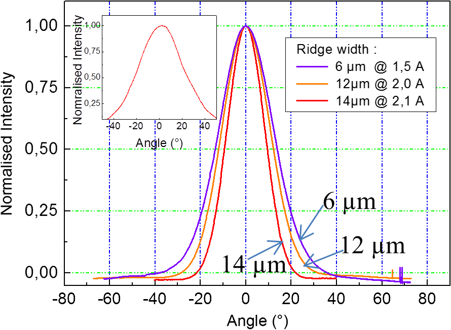 We also analyzed the maximum output power and WPE for all the lasers characterized. This is summarized in Table 1. All these were computed for one facet only. Table 1Summary of the buried heterostructure quantum cascade laser performance in terms of maximum output power and wall plug efficiency (WPE) for varying ridge widths.
All the characterized lasers were 5 mm long and HR-coated. High values of output power and WPE for the lasers suggest that the heat dissipation is very well facilitated due to the realization of the BH configuration. Although good, these results are not on par with those obtained by Bai et al.8 with regard to WPE. A few differences explain the discrepancy in terms of power and WPE. First of all, the number of periods in the structure is not the same, 30 periods versus 50 periods. The second difference comes from the mounting of the device, which implies that the thermal management of the chip is not as efficient and optimal in our case with respect to the one in Ref. 8. The last difference is the doping level, which is always different from one growth machine to another machine. This last variation will change the optimum length and width of the device for optimum power. The parametric study of the laser parameters versus efficiency could not be performed and the geometrical parameters of the chip are not optimum, whereas these have been optimized in the above-mentioned work. All those differences explain the differences in power and efficiency in the final device. Although the total power does not give insight into the efficiency of the lasers, this power value is very important since certain applications of these lasers usually require certain power, whatever may be the WPE. The important result here is that we have shown a single laser of 2.4 W output power in CW at room temperature with a far field in and no beam steering. Hence, our results are particularly interesting for useful applications. Finally, we compare the BH-QCLs [Fig. 1(a)] with ridge-alone QCLs [Fig. 1(b)] in terms of maximum output power at 10°C for different ridge widths. The results are shown in Fig. 9. Waveguide losses in this series could not be estimated by measuring the performance at different lengths due to the lack of enough material. Fig. 9Comparison of maximum output power for BH-QCL (as cleaved) and ridge-alone QCL (HR-coated). Measurements done at 20°C, with epi-side down mounting on identical AlN submounts. 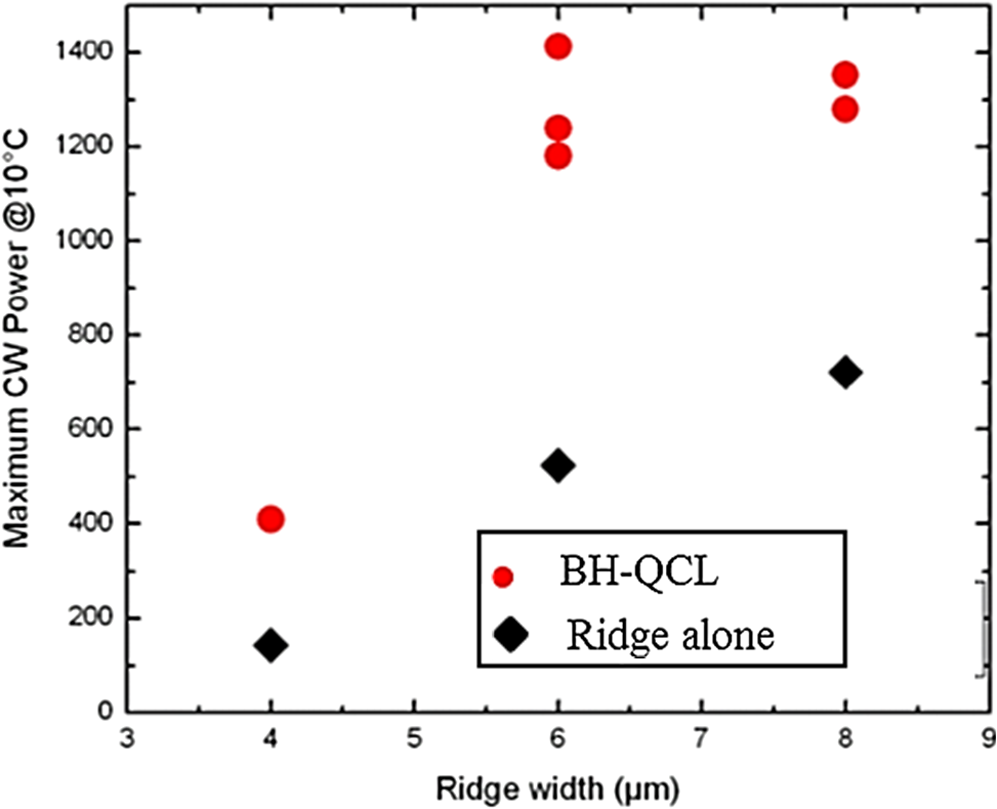 Note that the ridge-alone QCLs were HR-coated, but not the BH-QCLs. In spite of that, the BH-QCLs exhibit more than twice as much power as the ridge-alone QCL. It is known that thermal dissipation is anisotropic in the QCLs and the in-plane versus cross-plane ratio is typically around 2.5; higher in-plane conductivity is explained to be due to the bulk-like dispersion of phonons, whereas cross-plane dissipation is more complex in terms of phonon dispersion and can suffer largely from phonon reflections at the interfaces.27,28 It can even be expected that the lateral heat dissipation in a buried heterostructure can be reduced if the regrown interface is not seamless since it might also involve certain amount of phonon scattering. Thus, we have demonstrated that BH-QCL with a clean regrown interface is an effective way of gaining thermal benefits. 4.ConclusionsIn this study, we demonstrated a quick process to achieve BH-QCL, leading to high power and WPE. For this, we employed a hydride vapor phase epitaxy. With a single-step regrowth of highly resistive () semi-insulating InP:Fe in , BH-QCLs can be realized with burying ridges etched down to a 10- to depth. In addition, it has been shown that the current process is largely insensitive to the ridge profile and mask overhang and does not lead to rabbit ear growth near the ridge. HR-coated lasers emitting at and were characterized. The ridge width was very large in the former case and, hence, these were subjected to only pulsed operation. Both of them showed no leakage even at high currents. The latter were analyzed in depth with CW operation. Very reproducible results were obtained with the 5-mm-long lasers of ridge widths varying from 4 to . Besides being spatially monomode, , all the characterized lasers exhibited a WPE of to 9% with an output power of 1.5 to 2.5 W at room temperature and under CW operation. The performance can be further improved by using a material with a higher thermal conductivity for the submount, such as copper or diamond, and by employing facet coating. BH-QCLs were also compared with the ridge-alone QCLs and the former outperform the latter in their output power even though the latter were HR-coated and the former were only as-cleaved. Thus, the HVPE process is extremely suitable for mass production of high-performance QCLs. AcknowledgmentsThis work was supported by EU FP7 MIRIFISENS Integrated Project 317884. Linné Center of Excellence, ADOPT is also acknowledged. ReferencesR. F. KazarinovR. A. Suris,
“Possibility of the amplification of electromagnetic waves in a semiconductor with a superlattice,”
Sov. Phys. Semicond., 5
(4), 207
(1971). SPSEAX 0038-5700 Google Scholar
J. Faistet al.,
“Quantum cascade laser,”
Science, 264
(5158), 553
(1994). http://dx.doi.org/10.1126/science.264.5158.553 SCIEAS 0036-8075 Google Scholar
O. Cathabardet al.,
“Quantum cascade lasers emitting near ,”
Appl. Phys. Lett., 96
(14), 141110
(2010). http://dx.doi.org/10.1063/1.3385778 APPLAB 0003-6951 Google Scholar
C. Waltheret al.,
“Quantum cascade lasers operating from 1.2 to 1.6 THz,”
Appl. Phys. Lett., 91
(13), 131322
(2007). http://dx.doi.org/10.1063/1.2793177 APPLAB 0003-6951 Google Scholar
M. Becket al.,
“Buried heterostructure quantum cascade lasers,”
Proc. SPIE, 3284 231
–236
(1998). http://dx.doi.org/10.1117/12.304449 PSISDG 0277-786X Google Scholar
M. Becket al.,
“Continuous wave operation of a mid-infrared semiconductor laser at room temperature,”
Science, 295
(5553), 301
–305
(2002). http://dx.doi.org/10.1126/science.1066408 SCIEAS 0036-8075 Google Scholar
F. Xieet al.,
“High-temperature continuous-wave operation of low power consumption single-mode distributed-feedback quantum-cascade lasers at ,”
Appl. Phys. Lett., 95 091110
(2009). http://dx.doi.org/10.1063/1.3216074 APPLAB 0003-6951 Google Scholar
Y. Baiet al.,
“Quantum cascade lasers that emit more light than heat,”
Nat. Photonics, 4
(9), 99
–102
(2010). http://dx.doi.org/10.1038/nphoton.2009.263 1749-4885 Google Scholar
L. Diehlet al.,
“High-temperature continuous wave operation of strain-balanced quantum cascade lasers grown by metal organic vapor-phase epitaxy,”
Appl. Phys. Lett., 89
(21), 081101
(2006). http://dx.doi.org/10.1063/1.2337284 APPLAB 0003-6951 Google Scholar
M. Chashnikovaet al.,
“Buried-heterostructure quantum-cascade laser overgrowth by gas-source molecular beam-epitaxy,”
Appl. Phys. Lett., 100
(21), 213504
(2012). http://dx.doi.org/10.1063/1.4719109 APPLAB 0003-6951 Google Scholar
M. P. Semtsivet al.,
“Semi-insulating InP:Fe for buried-heterostructure strain-compensated quantum-cascade lasers grown by gas-source molecular-beam epitaxy,”
J. Cryst. Growth, 378
(1), 125
–128
(2013). http://dx.doi.org/10.1016/j.jcrysgro.2012.12.079 JCRGAE 0022-0248 Google Scholar
L. Chenget al.,
“Analysis of InP regrowth on deep-etched mesas and structural characterization for buried-heterostructure quantum cascade lasers,”
J. Electron. Mater., 41
(3), 506
–513
(2012). http://dx.doi.org/10.1007/s11664-011-1793-8 JECMA5 0361-5235 Google Scholar
S. LourdudossO. Kjebon,
“Hydride vapour phase epitaxy revisited,”
IEEE J. Sel. Topics Quantum Electron., 3
(3), 749
–767
(1997). http://dx.doi.org/10.1109/2944.640630 IJSQEN 1077-260X Google Scholar
E. R. MessmerT. LindströmS. Lourdudoss,
“In-situ mesa etching and immediate regrowth in a hydride vapour phase epitaxy reactor for buried heterostructure fabrication,”
J. Crystal Growth, 210
(4), 600
–612
(2000). http://dx.doi.org/10.1016/S0022-0248(99)00633-8 JCRGAE 0022-0248 Google Scholar
C. A. Barrioset al.,
“Epitaxially regrown GaAs/AlGaAs laser mesas with semi-insulating GaInP:Fe and GaAs:Fe,”
J. Electron. Mater., 30
(8), 987
–991
(2001). http://dx.doi.org/10.1007/BF02657722 JECMA5 0361-5235 Google Scholar
W. Glewet al.,
“Thermal instability of InGaAs/InGaAsP quantumwells,”
in 3rd Int. Conf. on Indium Phosphide and Related Materials,
515
–518
(1991). Google Scholar
C. Gmachlet al.,
“Quantum cascade lasers with a heterogeneous cascade: two-wavelength operation,”
Appl. Phys. Lett., 79
(6), 572
–574
(2001). http://dx.doi.org/10.1063/1.1383806 APPLAB 0003-6951 Google Scholar
A. Hugiet al.,
“External cavity quantum cascade laser tunable from 7.6 to ,”
Appl. Phys. Lett., 95 061103
(2009). http://dx.doi.org/10.1063/1.3193539 APPLAB 0003-6951 Google Scholar
A. Bismutoet al.,
“Large cavity quantum cascade lasers with InP interstacks,”
Appl. Phys. Lett., 93
(23), 231104
(2008). http://dx.doi.org/10.1063/1.3042213 APPLAB 0003-6951 Google Scholar
R. Blanchardet al.,
“Double-waveguide quantum cascade laser,”
Appl. Phys. Lett., 100
(3), 033502
(2012). http://dx.doi.org/10.1063/1.3678033 APPLAB 0003-6951 Google Scholar
J. Chenet al.,
“Monolithically integrated InP-based photonic chip development for O-CDMA systems,”
IEEE J. Sel. Topics Quantum Electron., 11
(1), 66
–77
(2005). http://dx.doi.org/10.1109/JSTQE.2004.841710 IJSQEN 1077-260X Google Scholar
S. J. B. YooS. LourdudossW. T. Tsang,
“Planar regrowth simplifies photonic integration of InP chips,”
Compd. Semicond., 15
(2), 14
–16
(2009). COSEFP Google Scholar
S. LourdudossO. Kjebon,
“Transverse structure optmisation in buried heterostructure lasers,”
Electrochem. Soc. Proc., 98-12 277
–287
(1998). Google Scholar
S. Blaseret al.,
“Room-temperature, continuous-wave, single-mode quantum-cascade lasers at ,”
Appl. Phys. Lett., 86
(4), 041109
(2005). http://dx.doi.org/10.1063/1.1853511 APPLAB 0003-6951 Google Scholar
Y. Baiet al.,
“Highly temperature insensitive quantum cascade lasers,”
Appl. Phys. Lett., 97
(25), 251104
(2010). http://dx.doi.org/10.1063/1.3529449 APPLAB 0003-6951 Google Scholar
G. M. de Nauroiset al.,
“High thermal performance of -stripes quantum cascade laser,”
Appl. Phys. Lett., 101
(4), 041113
(2012). http://dx.doi.org/10.1063/1.4739004 APPLAB 0003-6951 Google Scholar
A. LopsV. SpagnoloG. Scamarcio,
“Thermal modeling of GaInAs/AlInAs quantum cascade lasers,”
J. Appl. Phys., 100
(4), 043109
(2006). http://dx.doi.org/10.1063/1.2222074 JAPIAU 0021-8979 Google Scholar
S. Dhillonet al.,
“Ultra threshold current terahertz quantum cascade double-metal buried strip waveguides,”
Appl. Phys. Lett., 87
(7), 071107
(2005). http://dx.doi.org/10.1063/1.2001159 APPLAB 0003-6951 Google Scholar
BiographyWondwosen Metaferia has been a PhD student in the Department of Semiconductor Materials at the Royal Institute of Technology since 2010. He received his BSc and MSc in applied physics from Addis Ababa University, Ethiopia, in 2005 and 2007, respectively, and a MSc in photonics from Ghent University, Belgium, and Royal Institute of Technology, Sweden, in 2009. His research interests include III-V epitaxy, quantum cascade lasers, and characterizations of semiconductor materials and devices. Bouzid Simozrag started as a chemist in 1999. Then he was in charge of wafer processing of pump laser in ALCATEL Optronics in 2001 for three years. He received a master’s degree in materials sciences in Paris VII University in 2005. In 2006, he was in charge of the four-inches GaAs wafers (transistors) in United Monolithic Semiconductors. Since 2008, he has been in charge of quantum cascade laser (QCL) wafer processing in III-V Lab. Carl Junesand is a member of the technical staff at the Department of Semiconductor Materials at the Royal Institute of Technology as well as one of the cofounders of research-based spin-off company Epiclarus AB. His interests include III-V epitaxy, advanced photonic components, such as quantum cascade lasers, and silicon photonics. He received his PhD and MSc from the Royal Institute of Technology in 2013 and 2008, respectively. Yan-Ting Sun received his MSc from Linköping University in 1998, and his PhD from KTH-Royal Institute of Technology in 2003. From 2004 to 2011, he conducted research and development of high-power semiconductor lasers and avalanche photodiodes in several start-up companies. He joined the Laboratory of Semiconductor Materials in KTH-Royal Institute of Technology in 2011 as a researcher. His research interests include advanced semiconductor materials and photonic devices for communication and renewable energy. Mathieu Carras did his PhD degree in solid-state physics at the University of Paris 7 between 2003 and 2005. He got a permanent position in Alcatel Thales III-V Lab in 2006 on modeling, design, and characterization of QCLs. His current interests include mid- and far-infrared QCLs and quantum infrared detectors (QWIPs, QCDs). He has headed the team developing mid-infrared lasers at III-V Lab since 2011. Romain Blanchard received his MS from the Ecole Polytechnique, Paris, France, in 2008 and then joined the group of Professor Federico Capasso at Harvard University, where he completed his doctorate degree in 2013. His PhD research focused on wavelength control and beam engineering of QCLs and also involved a broad range of topics, including nano-optics, plasmonics, thin films, and energy harvesting. He joined Eos Photonics Inc. in 2013 as a senior scientist. Federico Capasso is the Robert Wallace professor of applied physics at Harvard University, where he joined in 2003 after a 27-year career at Bell Labs. His research has spanned electronics, photonics, plasmonics, metamaterials, and quantum electrodynamics. He is a coinventor of the quantum cascade laser. He is a member of the National Academy of Sciences and the National Academy of Engineering, and a recipient of the King Faisal Prize and the IEEE Edison Medal. Sebastian Lourdudoss joined KTH, Sweden, in 1980, after completing his MSc in chemistry in India in 1976 and PhD in physical chemistry in France in 1979. Since 1985, he has been involved in the vapor phase epitaxy of compound semiconductors for device fabrication. His expertise includes advanced epitaxial methods, nanofabrication, buried heterostructure lasers, photonic integration, and hetero-epitaxial solutions for III-Vs on Si. He is the head of the Department of Materials and Nano Physics at KTH. |