|
|
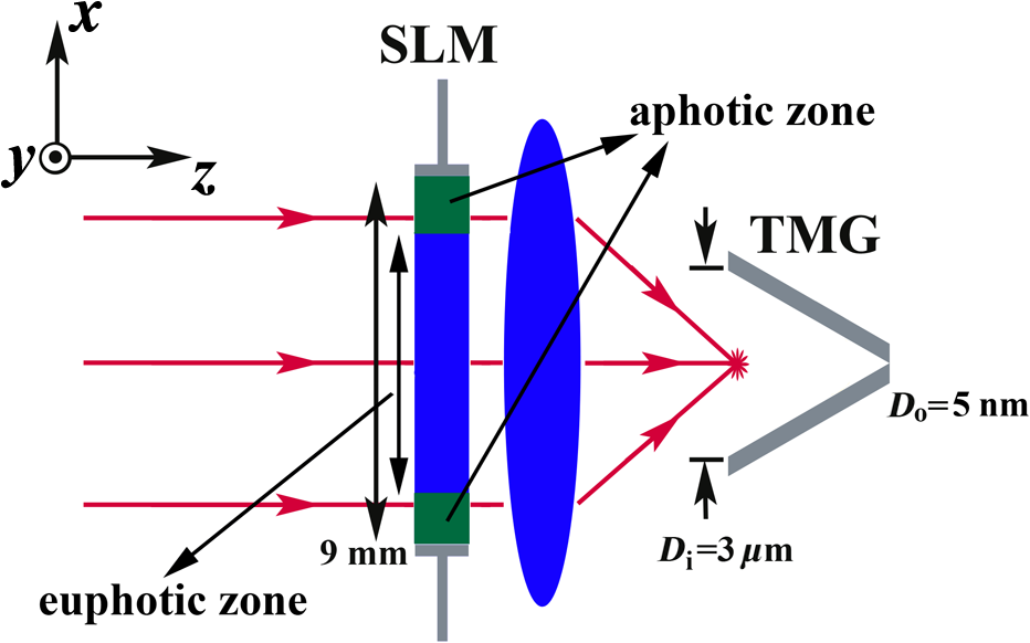
1.IntroductionEffectively obtaining a small-size transmission light field of high-power density is a crux of nanophotonics. Related technologies have been widely applied in super-resolution optical imaging,1 optical sensing,2 optical trapping and manipulation of particles,3 optical interconnection,4 high-density optical storage,5 nanolithography,6 solar energy utilization,7 local nonlinearity,8 and so on. An evanescent decay method based on a tapered metallic waveguide is most commonly adopted for this end.1 Compared with other methods, a small-size transmission light field obtained by this means exhibits the advantages of low background noise, immunity to external disturbance, and controllable size due to the shielding effect of the metal coating. But the transmission field at the aperture is derived from the evanescent radiation of light which is originated from the cutoff of the lowest propagating mode , and the light field intensity at the aperture will decrease sharply with the reduction of the aperture, so we can only obtain a subwavelength transmission field with a relatively low power.1 Recently, particular attention was given to tapered metal-insulator-metal (MIM) plasmonic waveguides such as tapered transmission lines,9 tapered gaps,10 tapered V-grooves,11 and nanocampanile (or three-dimensional linear taper),12,13 since they allow optical mode volumes to be confined to deep subwavelength dimensions via exciting and compressing gap surface plasmons (GSPs). However, GSPs in tapered MIM plasmonic waveguides are generally excited by the lowest propagating () mode using the fire-end coupling method through bulk light or guided modes coupling.14,15 To reduce the reflection and scattering losses and to transfer most of incident optical energy to the mode, the taper angles and the input entrance sizes of tapered MIM structures are generally smaller than the critical taper angle (usually less than 10 deg to meet the adiabatic conditions) and the wavelength of the input beam, respectively.14,15 This increases the difficulty of preparation of the MIM structure waveguide. But the input light field is not easy to be accurately projected into the input entrance of such MIM structure under a tightly focused condition. Therefore, the premise conditions of small taper angle and small-scale input entrance become an obstacle for the design and application of tapered plasmonic waveguides for field enhancement (FE) and nanofocusing. Butt-coupling from TM dielectric waveguides to MIM plasmonic waveguides is widely developed to improve the coupling efficiencies and a coupling efficiency as high as 70% was obtained.16–19 On the other hand, spatial light modulation has been widely used in optical research such as optical tweezers,20 mode analysis,21 ultrafast pulse shaping,22 active control of plasmonic field,23 perfect focusing of disorder scattering,24 optical vortex,25 nonlinear beam combing,26 and so on. Its ability to dynamically modulate the phase, amplitude, and polarization of an incident optical field shows the potential for controlling the optical field propagation inside tapered MIM plasmonic waveguides. In this paper, we propose a spatial amplitude modulation method to improve the light field coupling efficiency of a tapered metallic gap (TMG) with a large taper angle and large-scale input entrance. The influences of critical parameters, such as incident beam width (BW), incident wavelength, numerical aperture (NA) of the coupling lens, and the physical mechanism, are discussed, respectively. The optical FE of the TMG is improved greatly and an FE of about 3318 can be obtained through optimizing the relevant parameters (compared with the situation without amplitude modulation, the light coupling efficiency is increased by 16.43-fold). 2.Model and MethodThe schematic diagram of a TMG is illustrated in Fig. 1. The structure of the TMG is assumed to be uniform and infinite in the direction. Aluminum, which has a smaller skin depth than noble metals, is chosen as the metallic material for preventing optical leakage. The metal thickness , entrance width , aperture width , and taper angle of the TMG are 100 nm, , 5 nm, and 60 deg, respectively. The incident light is a linear TM-polarized Gaussian beam at a wavelength of with a BW of 9 mm, which propagates through an amplitude-only spatial light modulator (SLM) of a 9-mm aperture diaphragm (AD) before coupling into the TMG by a focusing lens (FL). The NA of the FL is 0.75 and the focal spot is assumed to be exactly located at the input entrance of the TMG. The amplitude modulation is carried out via controlling the central euphotic zone size of the SLM (as shown in Fig. 1). The optical evolution in the TMG is simulated with our self-developed finite-difference time-domain (FDTD) numerical model based on MATLAB language.10 In the FDTD calculations, the grid cell is and an anisotropic perfectly matched layer absorbing boundary condition is adopted for the truncation of FDTD lattices. The dielectric constant of aluminum is set as at according to the Lorentz–Drude model presented by Rakic et al.27 Unless otherwise specified, the following calculations are based on the above parameter values. 3.Results and DiscussionTo obtain insight into the physical nature of the improvement of the coupling efficiency, the distributions of the electric fields in the TMG with and without amplitude modulation are shown in Fig. 2. The euphotic zone size is after optimization calculation, and the other relevant parameters are chosen the same as those stated in Fig. 1 (, , ). The focusing field at the input entrance of the TMG is basically the diffraction light field of the SLM. Without amplitude modulation, the electric field components Ex in the TMG are shown in Fig. 2(a). The results demonstrate that the tightly focused optical field is strongly dispersed in free space, so higher order propagating modes are mainly excited in the TMG and most optical energy is reflected back or absorbed by the metallic walls. As a result, only a small amount of energy is transferred to the mode and an FE of only about 202 is obtained. The results indicate that the surface plasmons cannot be efficiently excited by the coupling without amplitude modulation. With amplitude modulation, the situation is completely different. In this case, the focusing field is evolved into a submicrometer collimated beam in free space, so the light energy reflected and absorbed by the metallic walls is small and most of the light energy in TMG is transferred to the mode [as shown in Fig. 2(b)]. Consequently, the coupling efficiency is improved by 4.53-fold and a high FE of about 916 is obtained. Fig. 2Distributions of the electric field component Ex in the TMG (, , ): (a) without and (b) with the amplitude modulation. 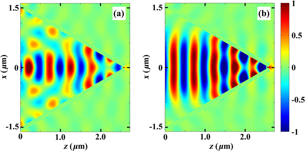 Figure 3 shows the FE as a function of the euphotic zone size for various BWs. On one hand, by varying the euphotic zone size from 0.2 to 9.0 mm, the distribution and transmission characteristics of the diffraction light field are changed regularly. The FE regularly fluctuates accordingly and the maximum FE is obtained when the euphotic zone size is about 1.8 mm. The results also indicate that the euphotic zone sizes at peak FEs are independent of the BW, because the coherence and destructive positions of the diffraction light field of the SLM are mainly determined by the euphotic zone size. On the other hand, with the increase of the light BW, the peak values of the FE curve increase accordingly. When the light BW increases to 13.0 mm, the improvement of the FE tends to be saturated. A maximum FE of about 973 can be obtained as the light BW increases to 13.0 mm. This demonstrates that when the incident BW approaches or even exceeds the AD size (9 mm), the incident beam is approximately equivalent to a parallel beam for the AD and a parallel beam is most beneficial to be collimated into a submicrometer beam with amplitude modulation. Fig. 3FE as a function of the euphotic zone size for various BWs (the other parameters are the same as those stated in Fig. 1). 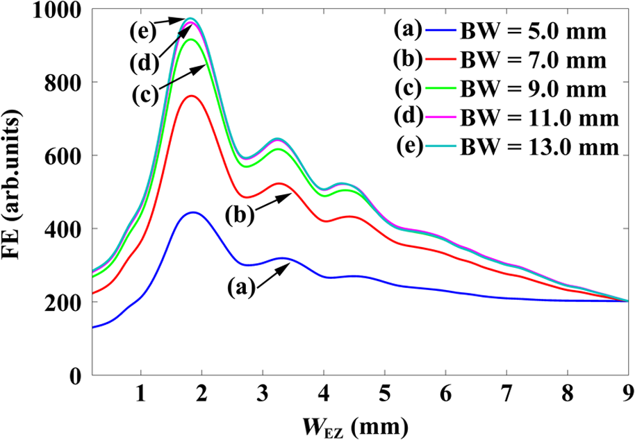 Figure 4 shows the FE as a function of the euphotic zone size for various NAs. By increasing the NA of the FL from 0.55 to 0.95 (we choose the NA values which can be realized at the general conditions with optical lens system), the whole FE curve moves up and a larger NA has a greater constructive impact on the improvement of the FE. As a result, a maximum FE of about 3318 is obtained as the NA of the FL increases to 0.95 (compared with the situation without amplitude modulation, the light coupling efficiency is increased by 16.43-fold). The results indicate that an NA value could yield an even higher FE. At the same time, with the increase of the NA from 0.55 to 0.95, the euphotic zone sizes corresponding to each peak FEs of the FE curve reduce accordingly. So for a larger NA, the maximum FE corresponds to a smaller euphotic zone size. It is clear that a larger NA is constructive for obtaining a smaller diffraction light field of higher intensity, and on the other side, it is well known that a narrower slit results in a wider diffraction field. The left shift of the corresponding peaks with the increase of the NA is the result of the balance of these two effects. Fig. 4FE as a function of the euphotic zone size for various NAs (the other parameters are the same as those stated in Fig. 1). 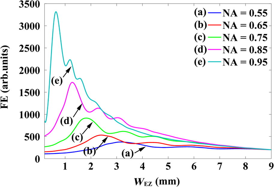 Figure 5 shows the FE as a function of the euphotic zone size for various incident wavelengths. By varying the incident wavelength from 400 to 600 nm, the FE as a function of the euphotic zone size decreases and a shorter wavelength is conducive to obtaining a larger FE. Obviously, short wavelength light field excitation results in a larger GSP propagation constant, which is advantageous for the compression and localization of the GSPs, so the FE curve drops accordingly with the increase of the incident wavelength. On the other side, the change of the FE curve becomes inconsiderable and the influence of incident wavelength tends to be saturated when the wavelength increases to 600 nm. We think that this phenomenon should be closely associated with the relationship between the focusing spot size and the incident wavelength. It is clear that the focusing spot size is in proportion to the incident wavelength and a short wavelength is more conducive for focusing via coupling lens. With the increase of the incident wavelength, the focusing spot size can be bigger than the input entrance of the TMG and under the circumstances the input entrance is equivalent to being uniformly illuminated by a parallel light, so the influence of the incident wavelength tends to be saturated. Fig. 5FE as a function of the euphotic zone size for various incident wavelengths (the other parameters are the same as those stated in Fig. 1). 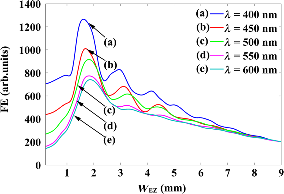 Finally, it must be pointed out that finding an optimal scheme of spatial amplitude modulations to improve the light field coupling efficiency of the TMG should be virtually difficult, since there are complicated inherent relationships between the euphotic zone size, the incident BW, the NA of the FL, and the incident wavelength. Our scheme is relatively simple and easy to operate. 4.ConclusionsIn summary, we demonstrate that the light field coupling efficiency of a TMG with a large taper angle and input entrance size can be markedly improved via spatial amplitude modulation of the incident beam. The improvement of the light field coupling efficiency is deeply influenced by the incident BW, the NA, of the FL and the incident wavelength. The physical mechanism of the coupling efficiency improvement is that with spatial amplitude modulation, the focusing field of the FL is evolved into a submicrometer collimated beam in free space, so most of the light energy transferring to the mode results in higher surface plasmon excitation efficiency. The substantial improvement of the light field coupling efficiency of TMGs with a large taper angle and entrance port size shows the potential in designing tapered MIM waveguides for FE and nanofocusing. AcknowledgmentsThe authors thank Dr. Li Li for useful discussion. This work was supported by the Chinese National Natural Science Foundation (61475038, 61205018, and 11404067) and by the Open Fund of the State Key Laboratory of Surface Physics, Fudan University (KF201305). ReferencesL. NovotnyB. Hecht, Principles of Nano-optics, Cambridge University Press, New York
(2006). Google Scholar
A. LeungP. M. ShankarR. Mutharasan,
“A review of fiber-optic biosensors,”
Sens. Actuators, B, 125
(2), 688
–703
(2007). http://dx.doi.org/10.1016/j.snb.2007.03.010 SABCEB 0925-4005 Google Scholar
B. H. Liuet al.,
“Nano-manipulation performance with enhanced evanescent field close to near-field optical probes,”
Opt. Commun., 284
(12), 3039
–3046
(2011). http://dx.doi.org/10.1016/j.optcom.2011.02.023 OPCOB8 0030-4018 Google Scholar
J. Shuet al.,
“Efficient coupler between chip-level and board-level optical waveguides,”
Opt. Lett., 36
(18), 3614
–3616
(2011). http://dx.doi.org/10.1364/OL.36.003614 OPLEDP 0146-9592 Google Scholar
P. Leiprechtet al.,
“Exploiting optical near fields for phase change memories,”
Appl. Phys. Lett., 98
(1), 013103
(2011). http://dx.doi.org/10.1063/1.3533395 APPLAB 0003-6951 Google Scholar
F. Huoet al.,
“Beam pen lithography,”
Nat. Nanotechnol., 5 637
–640
(2010). http://dx.doi.org/10.1038/nnano.2010.161 1748-3387 Google Scholar
Y. LiuR. HuangC. K. Madsen,
“Design of a lens-to-channel waveguide system as a solar concentrator structure,”
Opt. Express, 22
(S2), A198
–A204
(2014). http://dx.doi.org/10.1364/OE.22.00A198 OPEXFF 1094-4087 Google Scholar
I. Y. Parket al.,
“Plasmonic generation of ultrashort extreme-ultraviolet light pulses,”
Nat. Photonics, 5 677
–681
(2011). http://dx.doi.org/10.1038/nphoton.2011.258 1749-4885 Google Scholar
M. Schnellet al.,
“Nanofocusing of mid-infrared energy with tapered transmission lines,”
Nat. Photonics, 5 283
–287
(2011). http://dx.doi.org/10.1038/nphoton.2011.33 1749-4885 Google Scholar
Y. Chenet al.,
“Nanofocusing via efficient excitation surface plasmon polaritons in a hollow aluminum wedge,”
IEEE Photonics Technol. Lett., 25
(10), 929
–931
(2013). http://dx.doi.org/10.1109/LPT.2013.2256119 IPTLEL 1041-1135 Google Scholar
S. I. BozhevolnyiK. V. Nerkararyan,
“Adiabatic nanofocusing of channel plasmon polaritons,”
Opt. Lett., 35
(4), 541
–543
(2010). http://dx.doi.org/10.1364/OL.35.000541 OPLEDP 0146-9592 Google Scholar
W. Baoet al.,
“Mapping local charge recombination heterogeneity by multidimensional nanospectroscopic imaging,”
Science, 338 1317
–1321
(2012). http://dx.doi.org/10.1126/science.1227977 SCIEAS 0036-8075 Google Scholar
H. Chooet al.,
“Nanofocusing in a metal-insulator-metal gap plasmon waveguide with a three-dimensional linear taper,”
Nat. Photonics, 6 838
–844
(2012). http://dx.doi.org/10.1038/nphoton.2012.277 1749-4885 Google Scholar
D. K. GramotnevS. I. Bozhevolnyi,
“Nanofocusing of electromagnetic radiation,”
Nat. Photonics, 8 13
–22
(2014). http://dx.doi.org/10.1038/nphoton.2013.232 1749-4885 Google Scholar
D. F. P. PileD. K. Gramotnev,
“Adiabatic and nonadiabatic nanofocusing of plasmons by tapered gap plasmon waveguides,”
Appl. Phys. Lett., 89
(4), 041111
(2006). http://dx.doi.org/10.1063/1.2236219 APPLAB 0003-6951 Google Scholar
L. ChenJ. ShakyaM. Lipson,
“Subwavelength confinement in an integrated metal slot waveguide on silicon,”
Opt. Lett., 31
(14), 2133
–2135
(2006). http://dx.doi.org/10.1364/OL.31.002133 OPLEDP 0146-9592 Google Scholar
G. VeronisS. Fan,
“Theoretical investigation of compact couplers between dielectric slab waveguides and two-dimensional metal-dielectric-metal plasmonic waveguides,”
Opt. Express, 15
(3), 1211
–1221
(2007). http://dx.doi.org/10.1364/OE.15.001211 OPEXFF 1094-4087 Google Scholar
R. YangM. A.G. AbushagurZ. Lu,
“Efficiently squeezing near infrared light into a 21 nm-by-24 nm nanospot,”
Opt. Express, 16
(24), 20142
–20148
(2008). http://dx.doi.org/10.1364/OE.16.020142 OPEXFF 1094-4087 Google Scholar
R. Yanget al.,
“Efficient light coupling between dielectric slot waveguide and plasmonic slot waveguide,”
Opt. Lett., 35
(5), 649
–651
(2010). http://dx.doi.org/10.1364/OL.35.000649 OPLEDP 0146-9592 Google Scholar
K. DholakiaT. Cizmar,
“Shaping the future of manipulation,”
Nat. Photonics, 5 335
–342
(2011). http://dx.doi.org/10.1038/nphoton.2011.80 1749-4885 Google Scholar
D. Flammet al.,
“Mode analyses with a spatial light modulator as a correlation filter,”
Opt. Lett., 37
(13), 2478
–2480
(2012). http://dx.doi.org/10.1364/OL.37.002478 OPLEDP 0146-9592 Google Scholar
J. Lianget al.,
“High-precision laser beam shaping using a binary-amplitude spatial light modulator,”
Appl. Opt., 49
(8), 1323
–1330
(2010). http://dx.doi.org/10.1364/AO.49.001323 APOPAI 0003-6935 Google Scholar
B. Gjonajet al.,
“Active spatial control of plasmonic fields,”
Nat. Photonics, 5 360
–363
(2011). http://dx.doi.org/10.1038/nphoton.2011.57 1749-4885 Google Scholar
I. M. VellekoopA. LagendijkA. P. Mosk,
“Exploiting disorder for perfect focusing,”
Nat. Photonics, 4 320
–322
(2010). http://dx.doi.org/10.1038/nphoton.2010.3 1749-4885 Google Scholar
M. R. Denniset al.,
“Isolated optical vortex knots,”
Nat. Phys., 6 118
–121
(2010). http://dx.doi.org/10.1038/nphys1504 NPAHAX 1745-2473 Google Scholar
P. Q. Zhanget al.,
“Phase controlled beam combining with nonlinear frequency conversion,”
Opt. Express, 18
(3), 2995
–2999
(2010). http://dx.doi.org/10.1364/OE.18.002995 OPEXFF 1094-4087 Google Scholar
A. D. Rakicet al.,
“Optical properties of metallic films for vertical cavity optoelectronic devices,”
Appl. Opt., 37
(22), 5271
–5283
(1998). http://dx.doi.org/10.1364/AO.37.005271 APOPAI 0003-6935 Google Scholar
BiographyYongzhu Chen is an assistant professor at Guangdong Polytechnic Normal University. He received his MS degree in optics from South China Normal University in 2003 and his PhD degree in optics from Sun Yat-Sen University in 2012. He is the author of more than 30 journal papers and his current research interests include near-field optics, plasmons, and supercontinuum. Xiangsheng Xie is a lecturer at Sun Yat-Sen University. He received his PhD degree in optics from Sun Yat-Sen University in 2010. He is the author of more than 30 journal papers and his current research interests include optical vector beam, near-field optics and microscopic. Gengyan Chen is a lecturer at Guangdong Polytechnic Normal University. He received his bachelor’s degree in physics from Shandong University in 2008 and his PhD degree in theoretical physics from Sun Yat-Sen University in 2013. He is the author of 8 journal papers and his current research interests include quantum optics, photonic crystals, and microcavities. Lina Guo is a lecturer at Guangdong Polytechnic Normal University. She received her MS and PhD degrees in optics from South China Normal University in 2007 and 2011 respectively. She is the author of more than 20 journal papers, and her current research interests include partially coherent vector beams, propogation and focusing of vector vortex beams, and confocal microscopy. Xusheng Lin is a professor at Guangdong Polytechnic Normal University. He received his Ms degree in nuclear physics from the Beijing Institute on Applied Physics and Computational Mathematics in 1990 and his PhD degree in optics from South China Normal University in 2012. He is the author of more than 40 journal papers. His current research interests include nanophotonics and silicon photonic devices. |