|
|
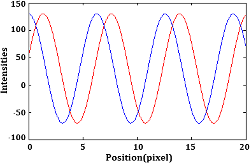
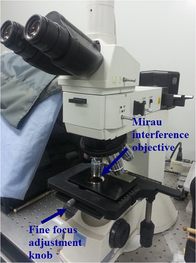
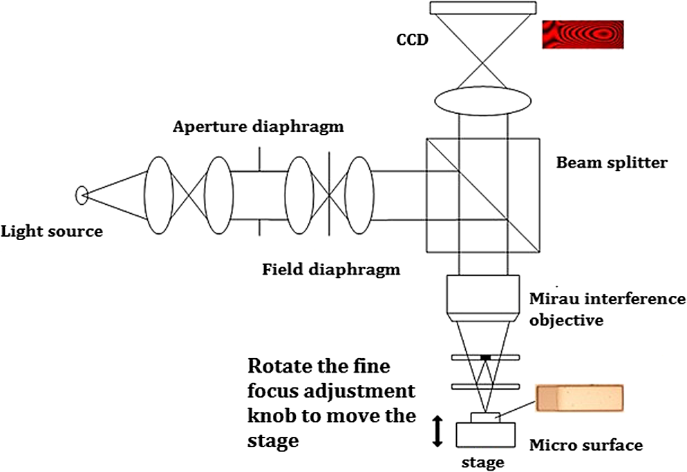
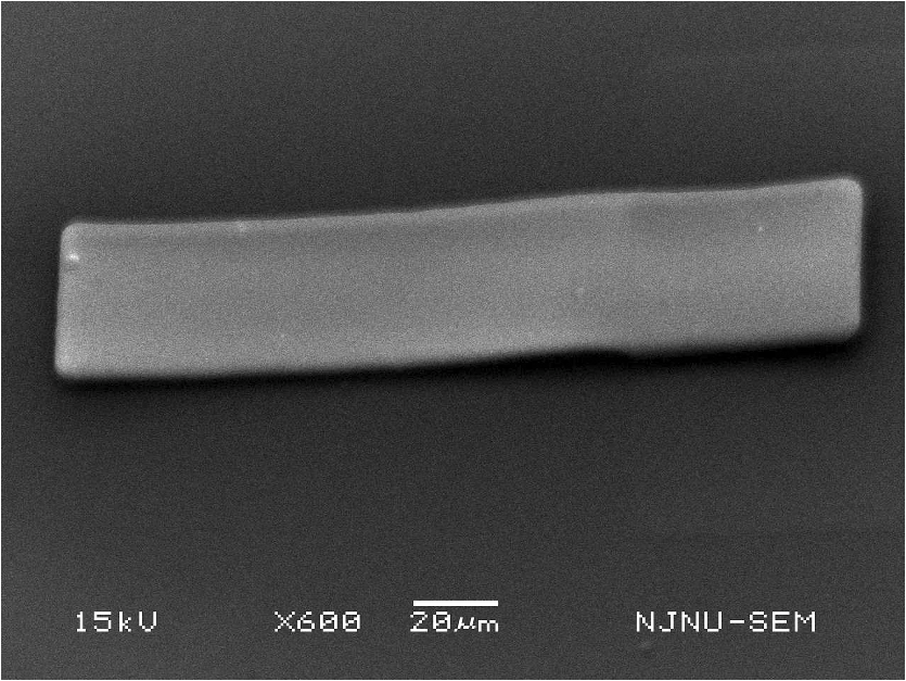
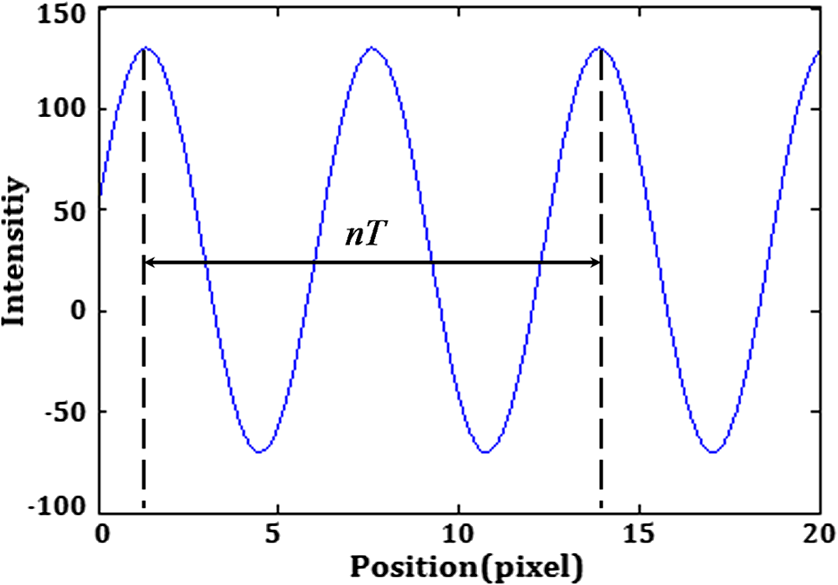
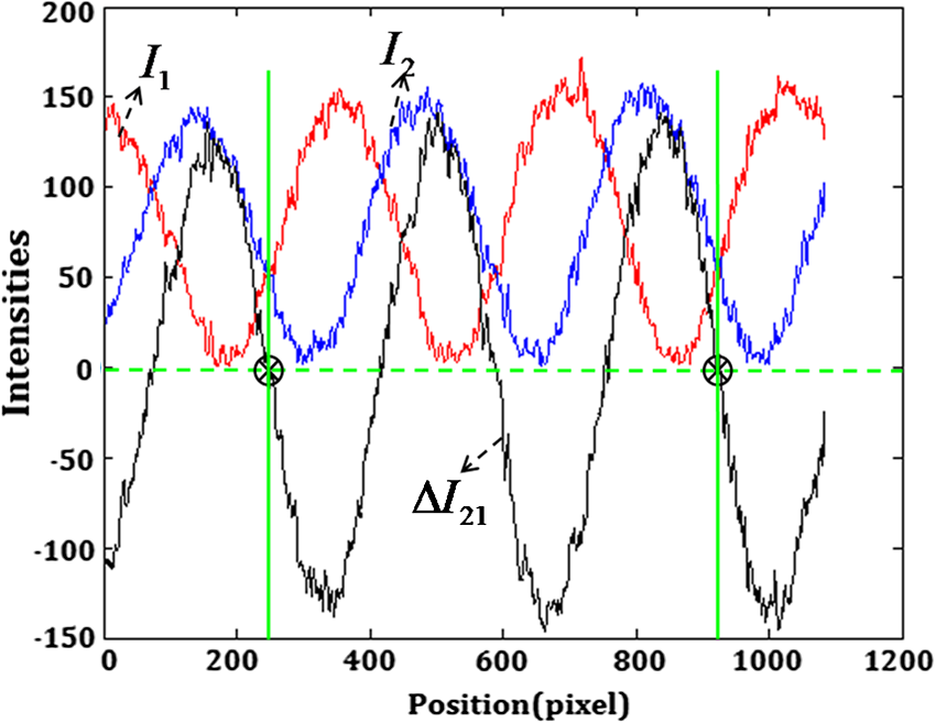
1.IntroductionWith the development of micro fabrication technology, accurate and simple three-dimensional MEMS surface topography metrology is becoming an urgent necessity.1 Because of the advantages of noncontact and high-precision, optical metrology2,3 has been widely applied in microsurface topography measurements such as phase-shifting interferometry(PSI),4–8 white light interferometry,9,10 heterodyne interferometry,11,12 phase-locked interferometry,13 and holography.14,15 Among these, PSI plays a very important role. In many earlier phase extraction algorithms that were based on PSI, such as the Carré algorithm,4 Stoilov algorithm,6 Schwider algorithm,7 and Hariharan algorithm,8 one had to know the amount of each shift with a high accuracy to reduce the effects of phase-shift errors; therefore, it usually required a high-precision phase-shifter which is very expensive.16 Meanwhile, on the assumption that only linear error exists in a phase shifter, a self-calibration algorithm was suggested by Carré4 and developed by Morgan17 and others. In this paper, based on the feature of MEMS structure which always has a plane substrate, a practical algorithm to calculate phase shifts from the gathered interference fringes of the substrate is presented, then microsurface topography can be reconstructed according to the obtained phase shifts. By means of the presented algorithm, an expensive and high-precision phase shifter is unnecessary and the phase-shift operation can even be carried out by rotating the fine focus adjustment knob. Obviously, it is useful for in situ MEMS topography measurement. 2.Principle2.1.Phase-Shift CalculationFigure 1 is a configuration of phase-shifting interferometry in which a piezoelectric transducer (PZT) is often used to move a reference mirror to induce a phase shift. The interferometer separates source light so that it follows two independent paths, one of which includes a reference mirror and the other includes the object surface. The separated light beams then recombine and interfere, and finally are directed to a digital camera which can record the resultant light intensity of each interferogram. Moving reference mirror by PZT, a phase shift is induced and the optical path difference of the two separated light beams is changed. Similarly, another interferogram that contains intensity distribution can be recorded. The intensity located at pixel of each interferogram can be expressed in the form where is the background intensity, is the modulation, is the phase to be determined, and is initial phase value.Usually, the substrate surface of a MEMS device is flat and smooth enough (in Fig. 1); therefore, the waveform of the interference intensity along any line on the substrate is a fine cosine function, as shown in Fig. 2. Considering two interferograms of a MEMS device surface obtained by a phase shift, the intensities can be represented as Along a line on the substrate, interference intensities of the two interferograms are cosine functions with the same period, as shown in Fig. 3. The initial phase values , can be calculated by fast Fourier transformation (FFT).18,19 The phase shift can be defined as Obviously, is also the phase shift value of every pixel of the test surface. 2.2.Algorithm of Phase DistributionComputing the phase distribution requires at least three interferograms. Existing literature6 has shown that increasing the number of interferograms can appropriately improve the accuracy of surface topography measurements. A five-step algorithm is given as where is the phase to be determined, and , , , , and are the initial phase values of the five interferograms, respectively.Note that , , and . Thus, Eqs. (5) to (9) can be rewritten as Now, in order to eliminate the parameter , the intensity difference can be represented as From Eqs. (15) and (16), we figure out the following equation where , ,Thus, Eq. (17) can be rewritten as Then further simplify Eq. (18) and the following two equations are obtained Finally, the wavefront phase is obtained where , , and are the phase shifts that can be calculated by the above mentioned method in Sec. 2.1.The wavefront phase obtained from Eq. (21) is wrapped phase which is often discontinuous and needs to be unwrapped as a continuous phase distribution . Then, the microsurface topography is obtained by where is the light wavelength and is a height function which relates to topography.3.Experiment and Results3.1.Experimental SetupThe experimental setup is a metallographic microscope (Type: Nikon-L150) whose objective is replaced by a Mirau interference objective (, Nikon), as shown in Figs. 4 and 5. The pixel size of the charge-coupled device (CCD) camera is , and the pixel number is . The light source wavelength is 633.3 nm. A micro structure, whose surface topography will be detected, is shown in Fig. 6. The detailed steps to record interferograms are as follows:
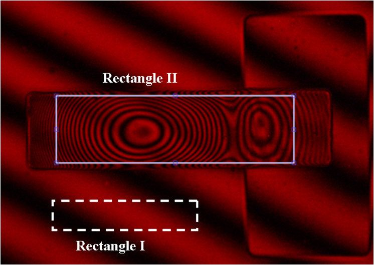
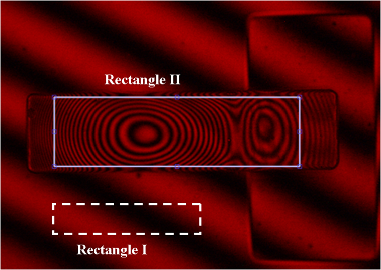
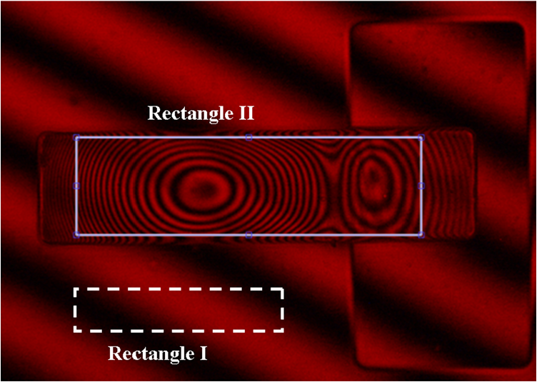
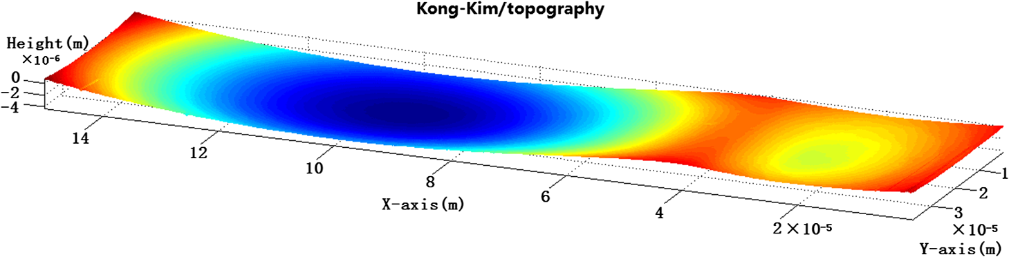
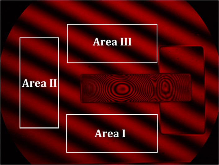
Following these steps, five interferograms are obtained which are shown in Figs. 7Fig. 8Fig. 9Fig. 10–11. 3.2.Topography ReconstructionIn order to reduce the influence of noise on the accuracy of the phase shift measurement, a rectangular region which contains many lines is selected (as shown in Figs. 7 through 11), then the average value of the phase shifts obtained from all lines in the rectangular region can be calculated and considered as the phase shift value of every pixel of the test surface; this is more accurate than that obtained from a single line. On the substrate area, respectively, select five rectangular regions (i.e., Rectangle I) at the same position on the five interferograms, as shown in Figs. 7 through 11. Using the above presented method, the actual phase shift values , , and also can be figured out by MATLAB®20 as Select the rectangular region (i.e., Rectangle II) in Figs. 7 through 11 as the test surface, then the test surface topography is reconstructed as shown in Fig. 12. 4.DiscussionThe optical resolution of the microscope is , and the actual length of a pixel is in the horizontal direction while the resolution in the vertical direction is 0.62 nm. The measurement resolution in the vertical direction is often defined by practical experiments. In the existing literature, In-bok Kong and Seung-Woo Kim presented a general algorithm of phase-shifting interferometry by iterative least-squares fitting18 which used the idea of iteration21–23 and had a rather high precision in the phase shift and topography measurement. Hence, the test surface topography, which is also mentioned in Sec. 3.2 and is reconstructed by the Kong-Kim algorithm, is given here, as shown in Fig. 13. From Figs. 12 to 13, it shows that the test surface topography which is reconstructed by the presented method is consistent with the reconstructed topography by the Kong-Kim algorithm. Meanwhile, the resulted phase shift values in the Kong-Kim algorithm can be compared with the calculated phase shift values in the presented method. Select three different regions in Fig. 14 on five corresponding interferograms (Figs. 7 through 11), then three sets of results which are obtained by, respectively, processing three regions of the interferograms as can be seen in Table 1. Table 1Error analysis of phase shift values.
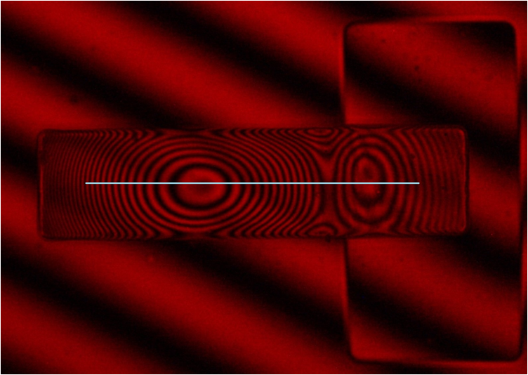
In Table 1, , , and are the absolute errors between the presented method (Five-step) and the Kong-Kim algorithm. From Table 1 and Fig. 14, we can see that whatever is images in Area I, Area II, or Area III, the absolute errors are very small. Especially in Area III where the light intensity is stronger, the absolute error is minimal among the three different regions mostly because it has a better signal-to-noise ratio. Moreover, in theory, the phase shift values are the same whatever is present in Area I, Area II, or Area III because the phase shifts are global. From Table 1, it is clear that the phase shift values which are calculated by the presented method are also nearly consistent. Thus, compared with Kong-Kim algorithm, the results from the presented method are better in the region where the light intensity is weaker (i.e., Area I and Area II), and the main reason is the presented method which is based on FFT can filter some noise in the phase-shift calculation and improve the precision of phase-shift calculation. Therefore, to obtain accurate phase shift values, it is necessary to process the good-quality regions of the obtained interferograms as far as possible.8,24 In order to evaluate the influence of the phase-shifting errors, we respectively adopt three sets of calculated phase shift values in Table 1 to reconstruct topography by processing a line in Fig. 15, and the results are shown in Fig. 16. Fig. 16Reconstructed topography and topography errors by three sets of phase shift values: (a) topography reconstructed by the calculated phase shift values in Area I; (b) relationships between topography errors and the calculated phase shift values in Area I; (c) topography reconstructed by the calculated phase shift values in Area II; (d) relationships between topography errors and the calculated phase shift values in Area II; (e) topography reconstructed by the calculated phase shift values in Area III; (f) relationships between topography errors and the calculated phase shift values in Area III. 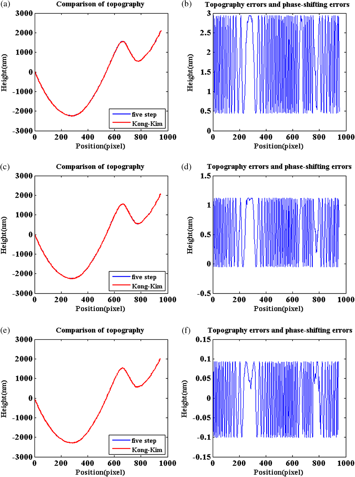 In Figs. 16(a), 16(c) and 16(e), it is clear that the results of topography which are reconstructed by using three sets of phase shift values in Table 1 are extremely overlapping. Since the phase-shifting error is minimal in Area III, the corresponding topography error also has a minimal value, which is about 0.1 nm, as shown in Fig. 16(f). Besides, the phase-shifting error is larger in Area I; therefore, the corresponding topography error has a bigger value which is about 3 nm, as shown in Fig. 16(b). In order to further improve the accuracy of the phase shift values, the initial phase should be precisely figured out as far as possible. As shown in Fig. 17, considering the feature of FFT, it is better to select complete periodic waveforms on the substrate. The method to select complete periodic waveforms is as follows:
The above-mentioned phase shift values are the pivotal factor that influences the presented algorithm. Additionally, there are some other error sources of the proposed method as follows:
5.ConclusionThe accuracy and feasibility of the method have been verified by experiments. The main advantages of the presented algorithm are as follows: (1) the algorithm can meet the accuracy requirement of the vast majority of MEMS topography measurements. (2) The speed of computation is faster than the iteration operation and initial values are unnecessary while inappropriate initial values can even lead to wrong results. (3) The phase-shift calculation is simple and the phase-shift operation does not require a high-precision PZT, just rotation of the fine focus adjustment knob; therefore, it makes the presented method more practical and meaningful. In a word, it is very suitable for in situ MEMS topography measurements. AcknowledgmentsThis research is sponsored by Nanjing Normal University and the Natural Science Foundation of the Jiangsu Higher Education Institutions of China (Grant No. 10KJA510024). ReferencesL. D. Chiffreet al.,
“Surfaces in precision engineering, micro-engineering and nanotechnology,”
Ann. CIRP, 52
(2), 561
–577
(2003). http://dx.doi.org/10.1016/S0007-8506(07)60204-2 0007-8506 Google Scholar
D. Malacara, Optical Shop Testing, 3rd ed.John Wiley & Sons, New York
(2007). Google Scholar
J. C. Wyant,
“Computerized interferometric surface measurements,”
Appl. Opt., 52
(1), 1
–8
(2013). http://dx.doi.org/10.1364/AO.52.000001 APOPAI 0003-6935 Google Scholar
P. Carré,
“Installation et utilisation du comparateur photoélectrique et interférentiel du Bureau International des Poids et Mesures,”
Metrologia, 2
(1), 13
–23
(1966). http://dx.doi.org/10.1088/0026-1394/2/1/005 MTRGAU 0026-1394 Google Scholar
B. BhushanJ. C. WyantC. L. Koliopoulos,
“Measurement of surface topography of magnetic tapes by Mirau interferometry,”
Appl. Opt., 24
(10), 1489
–1497
(1985). http://dx.doi.org/10.1364/AO.24.001489 APOPAI 0003-6935 Google Scholar
G. StoilovT. Drgaostinov,
“Phase-stepping interferometry: five frame algorithm with an arbitrary step,”
Opt. Laser Eng., 28
(1), 61
–69
(1997). http://dx.doi.org/10.1016/S0143-8166(96)00048-6 OLENDN 0143-8166 Google Scholar
J. Schwideret al.,
“Digital wave-front measuring interferometry: some systematic error sources,”
Appl. Opt., 22
(21), 3421
–3432
(1983). http://dx.doi.org/10.1364/AO.22.003421 APOPAI 0003-6935 Google Scholar
P. HariharanB. F. OrebT. Eiju,
“Digital phase-shifting interferometry: a simple error-compensating phase calculation algorithm,”
Appl. Opt., 26
(13), 2504
–2506
(1987). http://dx.doi.org/10.1364/AO.26.002504 APOPAI 0003-6935 Google Scholar
L. C. ChenM. T. LeY. S. Lin,
“3-D micro surface profilometry employing novel Mirau-based lateral scanning interferometry,”
Meas. Sci. Technol., 25
(9), 094004
(2014). http://dx.doi.org/10.1088/0957-0233/25/9/094004 MSTCEP 0957-0233 Google Scholar
J. C. Wyant,
“White light interferometry,”
Proc. SPIE, 4737 98
–107
(2002). http://dx.doi.org/10.1117/12.474947 PSISDG 0277-786X Google Scholar
J. E. Greivenkamp,
“Generalized data reduction for heterodyne interferometry,”
Opt. Eng., 23
(4), 350
–352
(1984). http://dx.doi.org/10.1117/12.7973298 OPEGAR 0091-3286 Google Scholar
T. Schuldtet al.,
“Picometre and nanoradian heterodyne interferometry and its application in dilatometry and surface metrology,”
Meas. Sci. Technol., 23
(5), 054008
(2012). http://dx.doi.org/10.1088/0957-0233/23/5/054008 MSTCEP 0957-0233 Google Scholar
G. W. JohnsonD. C. LeinerD. T. Moore,
“Phase-locked interferometry,”
Opt. Eng., 18
(1), 180146
(1979). http://dx.doi.org/10.1117/12.7972318 OPEGAR 0091-3286 Google Scholar
W. Chenet al.,
“Quantitative detection and compensation of phase-shifting error in two-step phase-shifting digital holography,”
Opt. Commun., 282
(14), 2800
–2805
(2009). http://dx.doi.org/10.1016/j.optcom.2009.04.025 OPCOB8 0030-4018 Google Scholar
W. ChenX. D. Chen,
“Quantitative phase retrieval of a complex-valued object using variable function orders in the fractional Fourier domain,”
Opt. Express, 18
(13), 13536
–13541
(2010). http://dx.doi.org/10.1364/OE.18.013536 OPEXFF 1094-4087 Google Scholar
R. LangojuA. PatilP. Rastogi,
“Statistical study of generalized nonlinear phase step estimation methods in phase-shifting interferometry,”
Appl. Opt., 46
(33), 8007
–8014
(2007). http://dx.doi.org/10.1364/AO.46.008007 APOPAI 0003-6935 Google Scholar
C. J. Morgan,
“Least-squares estimation in phase-measurement interferometry,”
Opt. Lett., 7
(8), 368
–370
(1982). http://dx.doi.org/10.1364/OL.7.000368 OPLEDP 0146-9592 Google Scholar
M. TakedaH. InaS. Kobayashi,
“Fourier-transform method of fringe-pattern analysis for computer-based topography and interferometry,”
J. Opt. Soc. Am., 72
(1), 156
–160
(1982). http://dx.doi.org/10.1364/JOSA.72.000156 JOSAAH 0030-3941 Google Scholar
K. A. GoldbergJ. Bokor,
“Fourier-transform method of phase-shift determination,”
Appl. Opt., 40
(17), 2886
–2894
(2001). http://dx.doi.org/10.1364/AO.40.002886 APOPAI 0003-6935 Google Scholar
R. C. Gonzalez, Digital Image Processing Using MATLAB, Prentice Hall, New Jersey
(2003). Google Scholar
I. B. KongS. W. Kim,
“General algorithm of phase-shifting interferometry by iterative least-squares fitting,”
Opt. Eng., 34
(1), 183
–188
(1995). http://dx.doi.org/10.1117/12.184088 OPEGAR 0091-3286 Google Scholar
H. W. GuoM. Y. Chen,
“Least-squares algorithm for phase-stepping interferometry with an unknown relative step,”
Appl. Opt., 44
(23), 4854
–4859
(2005). http://dx.doi.org/10.1364/AO.44.004854 APOPAI 0003-6935 Google Scholar
Y. JoonhoJ. K. Nam,
“Minimization of spectral phase errors in spectrally resolved white light interferometry by the iterative least-squared phase-shifting method,”
Meas. Sci. Technol., 23
(12), 125203
(2012). http://dx.doi.org/10.1088/0957-0233/23/12/125203 MSTCEP 0957-0233 Google Scholar
Y. Surrel,
“Additive noise effect in digital phase detection,”
Appl. Opt., 36
(1), 271
–276
(1997). http://dx.doi.org/10.1364/AO.36.000271 APOPAI 0003-6935 Google Scholar
BiographyXi Chen is pursuing his MS degree at Nanjing Normal University. In 2012, he graduated with a BS degree in electrical engineering. His current research interests include micro-electro-mechanical systems (MEMS) and optical engineering. Hua Rong is an associate professor at Nanjing Normal University. He received his BS and MS degrees from Xi’an Jiaotong University, China, in 1988 and 1999, respectively, and his PhD degree from Southeast University, China, in 2004, all in electrical engineering. His current research interests include micro-electro-mechanical systems (MEMS) and optical engineering. |
||||||||||||||||||||||||||||||||||||||||||||||||||||||||