|
|
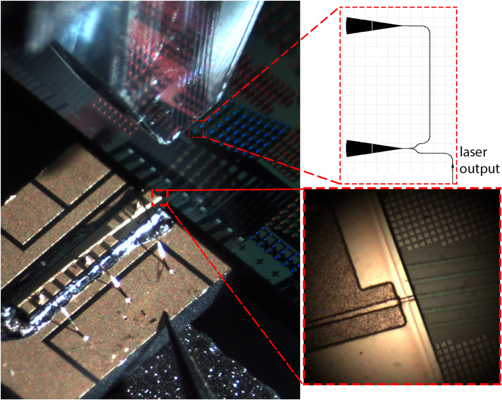
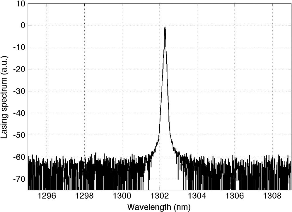
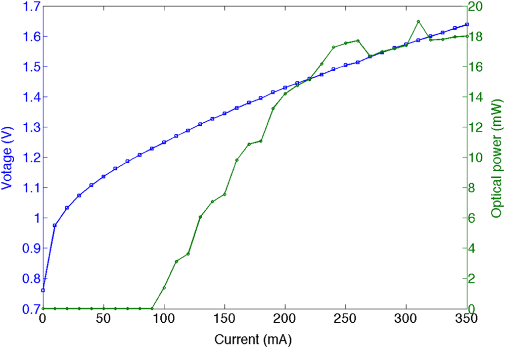
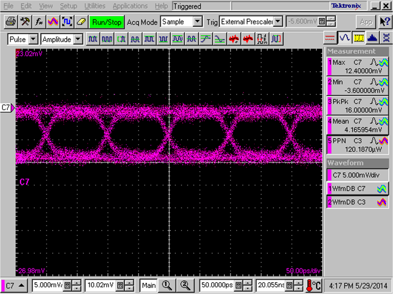
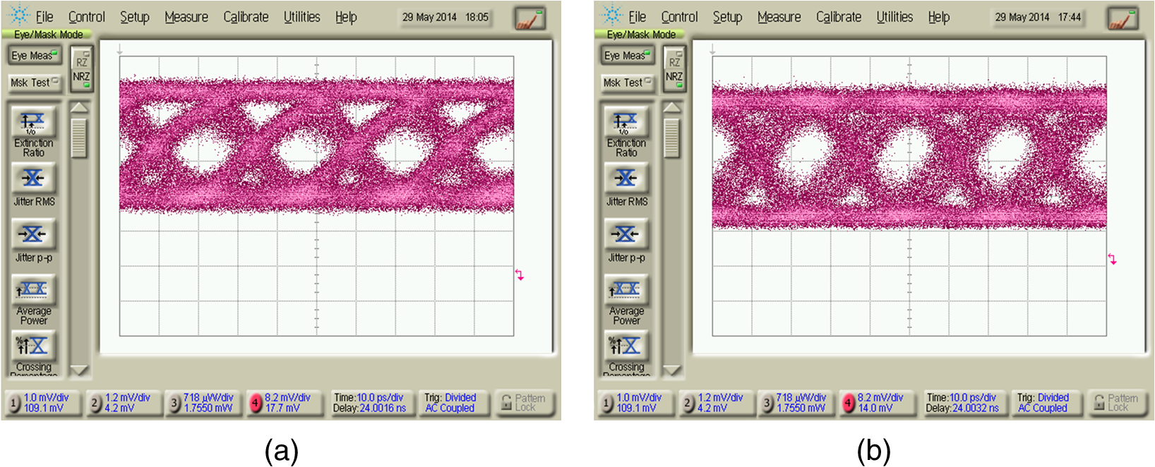
1.IntroductionDemand for Internet bandwidth continues to grow, due in large part to the increasing popularity of video services and mobile devices.1 Silicon photonics has attracted extensive academic and industrial attention as a solution for next-generation high-speed, low-energy consumption, and low-cost communication systems. The last decade witnessed tremendous enrichment and maturation of the silicon photonics device library, including high-performance passive components,2–4 silicon modulators,5 germanium on silicon photodetectors,6,7 and hybrid integrated lasers.8–11 Almost all silicon photonics devices demonstrated to date operate in the C-band (1530 to 1565 nm), which is within the fiber loss and erbium amplification window and is ideal for long-haul communications. However, for short reach interconnects such as interconnects in data centers, the O-band near 1310 nm is preferred to take advantage of the minimum dispersion window of standard optical fibers and is a widely used industry standard. It is possible to build silicon photonic components for the O-band by leveraging knowledge of C-band devices, since passive components can be easily redesigned by scaling the geometry, the free carrier plasma effect used for electro-optical modulation is wavelength insensitive, and germanium in photodetectors has stronger absorption at shorter wavelengths. We recently presented a set of O-band devices with a focus on a highly optimized waveguide crossing,12 except for the laser. Building an integrated O-band laser source is important to complete the library of integrated devices. In this paper, we report the first hybrid integrated external cavity laser consisting of a quantum dot (QD) reflective semiconductor optical amplifier (RSOA) and a silicon-on-insulator (SOI) chip. Lasing at 1302 nm with over 50-dB side-mode suppression ratio (SMSR) is observed. The FWHM line width is less than 330 kHz determined by heterodyne measurement. We also demonstrate open-eye data transmission at 10 and using this laser as the light source. 2.Device Design2.1.Gain Medium IntegrationAn appropriate gain medium must be used for building an O-band light source, since the gain spectra of typical materials cannot cover both 1310 and 1550 nm. A conventional indium phosphide (InP) quantum well-based gain medium could be used,13 but an InAs/GaAs QD gain medium gives unprecedented advantages, such as ultralow temperature dependence,14 low-noise single cavity multiwavelength lasing,15 and a wide tuning range.16 The fabrication and optical properties of silicon QDs were also reported, including optical amplification17–19 and all-optical modulation,20 which are promising for integration with silicon photonics devices. The wafer bonding approach in Ref. 13 mitigates alignment efforts since waveguides are lithographically defined, but reduces CMOS compatibility at the same time. QD lasers monolithically grown on silicon were also reported,21 but compatibility with integration of the rest of silicon photonics device library remains elusive. We choose the external cavity laser approach by edge coupling a QD RSOA and a silicon chip, both of which can be independently optimized without compromising the performance. State-of-the-art optoelectronic packaging process can be leveraged to cost effectively build the device. The diagram of our laser is shown in Fig. 1. The QD RSOA is based on indium arsenide QDs in gallium arsenide with aluminum gallium arsenide barriers and off-the-shelf commercially available components.22 Facet reflectivity is for the high reflective end and for the antireflective end, as specified by the manufacturer. The waveguide on the antireflective end is angled to reduce reflection into the laser cavity. Fig. 1Diagram of the hybrid external cavity laser. A quantum dot semiconductor optical amplifier is butt coupled to a silicon-on-insulator chip. The half-cavity on silicon consists of a Sagnac loop mirror and a microring wavelength filter. Grating couplers used for device characterization are also shown. 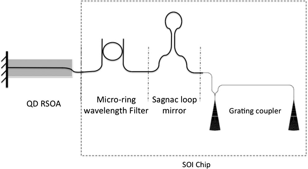 2.2.Silicon Chip LayoutOn the SOI chip, the silicon device layer is 220-nm thick. Five hundred nanometers of wide strip or rib waveguide is used for device layout and routing. The gap for evanescent coupling sections in the microring wavelength filter and Sagnac loop mirror is 200 nm edge-to-edge. The Sagnac loop is a simple and robust on-chip mirror for silicon photonics.23 Its reflectivity can be tuned by adjusting the directional coupler, which in this case is made from two long strip waveguides to provide about 50% reflection. The Lorentzian line shape of the ring resonator provides strong side mode suppression and helps linewidth reduction.24 The microring may also be used for wavelength tuning and stabilization.25 We used a microring of radius with a coupling region containing a long rib waveguide directional coupler. The rib waveguide is used for the ring as well to enable possible future electrode connections for wavelength tuning. The ring filter was measured to have an 8.8 nm free spectral range and 0.8 nm FWHM bandwidth. The cavity length is dominated by the off-the-shelf RSOA length of 3 mm, which could be customized shorter in the future. The current cavity length corresponds to about a 0.1 nm mode spacing, which is on the order of the FWHM of the microring filter. As shown in Fig. 1, the laser output is connected to a -junction and grating coupler. Grating couplers were used because the insertion loss of a grating coupler could be more accurately and easily characterized than an edge coupler for our setup. A grating coupler loop, compared to a single grating coupler, helps fiber array alignment and measurement of the grating coupler insertion loss. Insertion loss of the -junction is well characterized3 and could be easily normalized out. 2.3.Edge CouplingTo achieve a low coupling loss, light in the silicon waveguide is first coupled to a silicon nitride waveguide using an inverse taper coupler, similar to Ref. 26. The inverse taper waveguide coupler has about a 0.5 dB insertion loss. The silicon nitride waveguide is adiabatically tapered wider to match the RSOA mode size in the horizontal direction. In the vertical direction (normal to the wafer surface), 200 nm is too thin to provide effective mode confinement, and the modal field is extended into the oxide cladding to better match the RSOA mode. The nitride edge coupler mode size is designed to be to match typical SOA mode sizes. The 200-nm thick silicon nitride waveguide is less sensitive to fabrication errors compared to the 90-nm thick partially etched silicon waveguide we used in our previous work,11 and could also be used to build other devices, such as polarization splitter/rotators.27 3.Characterization and Discussion3.1.Testing SetupThe silicon chip was polished after wafer dicing to create a flat and smooth facet for butt coupling. No antireflective coating was applied on the silicon chip. Then both the RSOA and the silicon chip are mounted on six-axis stages for active alignment. The gain chip was kept at 25°C using a thermo-electric cooler, while the silicon chip was at the ambient temperature of the metal chuck. The RSOA and SOI chip were aligned to each other, and then the fiber array was aligned to grating couplers on the SOI chip, as shown in Fig. 2. The alignment procedure was described in more detail in the next section. 3.2.Alignment ProcedureAfter both anode and cathode probes were in contact with the corresponding metal pads on the RSOA and the pump current was flowing properly, a lensed fiber was brought near the high reflective end of the RSOA to monitor the cavity ASE or lasing condition as a feedback for the alignment. The silicon chip position was manually rastered until power in the lensed fiber was maximized. A big jump was observed when lasing started, and the power increased further as the silicon position was optimized. A bright spot at the output grating coupler was visible on an infrared camera at this step. We then temporarily turned off the laser pump current for grating coupler alignment. A fiber array was brought into proximity of the silicon chip surface to probe the grating coupler. The two pigtail fibers from the array are connected to an Agilent testing laser and power meter for active alignment. The fiber to chip coupling loss was determined to be 14 dB, which is less than optimal because we wanted to avoid perturbing the RSOA to silicon chip alignment. This can be improved in the future when the gain chip is securely bonded. Once the fiber array was aligned, the Agilent laser was turned off and the RSOA pump current for the device under test (DUT) was turned back on. Device characterization was performed under this condition. 3.3.Device CharacterizationThe output pigtail fiber was connected to an optical spectrum analyzer. The observed lasing spectrum is plotted in Fig. 3. The lasing peak appears at 1302 nm, with over 50 dB SMSR. We then performed a heterodyne measurement of the linewidth of this device. The laser output was combined with the output of another laser, HP 8167A, using a 3-dB fiber coupler. Then the combined optical signal was fed into a photodetector. The photo current was fed into a RF spectrum analyzer. The heterodyne beating spectrum is plotted in Fig. 4, along with a Lorentz fit. According to the fit, the FWHM of the combined linewidth of DUT and HP 8167A is 330 kHz. Fig. 4Heterodyne spectrum. Blue dots are experimental data, and black curve is a Lorentzian fit. The FWHM linewidth of the fit is 330 kHz. 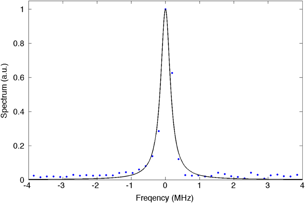 The light, voltage, and current characteristics of this device are summarized in Fig. 5. A clear threshold is observed at around 90 mA. Some kinks due to mode hoping when the current is swept are also visible on the LI curve, a common occurrence for hybrid external silicon lasers,8–11 but the kink near 250 mA is irregular and most likely due to mechanical or thermally induced alignment perturbations. The coupling loss between the silicon chip and RSOA is calculated to be 1.85 dB from the slope efficiency based on the theory in Ref. 28. The wall plug efficiency at 200 mA is 5%, which is comparable to the devices in the literature8–11 and could be further improved by adjusting the edge coupler to better match the mode and putting an antireflective coating on the silicon chip. 3.4.Data TransmissionTo further validate the viability of this device for data-com applications, we performed data transmission experiments at different data rates. The output of the DUT is first amplified and filtered, then modulated using a Lithium Niobate () Mach–Zehnder modulator. The nonreturn to zero modulated signal was received by a photodetector and displayed on a digital communication analyzer. At , a clean and open eye diagram was observed, as shown in Fig. 6, with an 8.7 dB extinction ratio, 50.92% cross-point percentage, and jitter of 11.19 ps. Figure 7 shows eye diagrams of our laser compared to a commercial DFB laser from Agere Systems (A1611A/B). Open eyes are observed showing suitable transmission, although with thicker lines and longer rise and fall times. Figure 7 also indicates that the test equipment, instead of the DUT, is limiting the speed. 3.5.DiscussionDevice spectrum and LIV characteristics demonstrated in the previous sections show our QD SOA/silicon external cavity device as an excellent O-band laser. The eye diagrams further validate its viability as a light source in data communication systems. The utilization of a QD SOA instead of a conventional quantum well or bulk SOA enables other attractive device properties. In the bulk material charge, carriers are continuously distributed to higher energy states as the temperature is raised. Injected carriers are confined in isolated energy states and no such redistribution can occur in zero-dimensional structures. As a result, QD lasers enjoy low threshold current and temperature dependence. In fact, the lowest threshold currents and highest operating temperatures of any semiconductor lasers belong to such QD lasers.29,30 To achieve a low threshold current in our external cavity laser, the coupling loss between the QD SOA and silicon chip needs to be further reduced, which can be achieved by customizing the spot size converters on both chips. For a wide operating temperature range, the SOA and silicon chip need to be securely bonded together using a glue or epoxy with a low thermal coefficient of expansion. Due to strong spectral hole burning, the QD material has a much lower mode partition noise, and a single cavity multiwavelength Fabry–Perot QD laser has been reported.15 Our external cavity QD SOA/silicon laser decouples the gain medium and cavity feedback, which provides further flexibility in the lasing wavelength and channel spacing selection. AcknowledgmentsThe authors would like to thank Gernot Pomrenke of AFOSR for his support of the OpSIS effort. The authors would also like to thank Mentor Graphics and Lumerical Solutions for their continuing support of the OpSIS project. We gratefully acknowledge support for this work by Portage Bay Photonics, LLC. ReferencesCisco white paper, “Cisco visual networking index: Global mobile data traffic forecast update, 2014–2019,”
(2015) February ). 2015). Google Scholar
W. Bogaerts et al.,
“Silicon-on-insulator spectral filters fabricated with CMOS technology,”
IEEE J. Sel. Top. Quantum Electron., 16
(1), 33
–44
(2010). http://dx.doi.org/10.1109/JSTQE.2009.2039680 IJSQEN 1077-260X Google Scholar
Y. Zhang et al.,
“A compact and low loss Y-junction for submicron silicon waveguide,”
Opt. Express, 21
(1), 1310
–1316
(2013). http://dx.doi.org/10.1364/OE.21.001310 OPEXFF 1094-4087 Google Scholar
S. Yang et al.,
“High efficiency germanium-assisted grating coupler,”
Opt. Express, 22
(25), 30607
–30612
(2014). http://dx.doi.org/10.1364/OE.22.030607 OPEXFF 1094-4087 Google Scholar
D. J. Thomson et al.,
“High performance Mach–Zehnder-based silicon optical modulators,”
IEEE J. Sel. Top. Quantum Electron., 19
(6), 3400510
(2013). http://dx.doi.org/10.1109/JSTQE.2013.2264799 IJSQEN 1077-260X Google Scholar
Y. Zhang et al.,
“A high-responsivity photodetector absent metal-germanium direct contact,”
Opt. Express, 22
(9), 11367
–11375
(2014). http://dx.doi.org/10.1364/OE.22.011367 OPEXFF 1094-4087 Google Scholar
L. Vivien et al.,
“Zero-bias germanium waveguide photodetector on silicon,”
Opt. Express, 20
(2), 1096
–1101
(2012). http://dx.doi.org/10.1364/OE.20.001096 OPEXFF 1094-4087 Google Scholar
T. Creazzo et al.,
“Integrated tunable CMOS laser,”
Opt. Express, 21
(23), 28048
–28053
(2013). http://dx.doi.org/10.1364/OE.21.028048 OPEXFF 1094-4087 Google Scholar
A. J. Zilkie et al.,
“Power-efficient III–V/silicon external cavity DBR lasers,”
Opt. Express, 20
(21), 23456
–23462
(2012). http://dx.doi.org/10.1364/OE.20.023456 OPEXFF 1094-4087 Google Scholar
S. Tanaka et al.,
“High-output-power, single-wavelength silicon hybrid laser using precise flip-chip bonding technology,”
Opt. Express, 20
(27), 28057
–28069
(2012). http://dx.doi.org/10.1364/OE.20.028057 OPEXFF 1094-4087 Google Scholar
S. Yang et al.,
“A single adiabatic microring-based laser in 220 nm silicon-on-insulator,”
Opt. Express, 22
(1), 1172
–1180
(2014). http://dx.doi.org/10.1364/OE.22.001172 OPEXFF 1094-4087 Google Scholar
Y. Zhang et al.,
“A compact and low-loss silicon waveguide crossing for O-band optical interconnect,”
Proc. SPIE, 8990 899002
(2014). http://dx.doi.org/10.1117/12.2037823 PSISDG 0277-786X Google Scholar
H.-H. Chang et al.,
“1310 nm silicon evanescent laser,”
Opt. Express, 15
(18), 11466
–11471
(2007). http://dx.doi.org/10.1364/OE.15.011466 OPEXFF 1094-4087 Google Scholar
M. Sugawara and M. Usami,
“Quantum dot devices: handling the heat,”
Nat. Photonics, 3 30
–31
(2009). http://dx.doi.org/10.1038/nphoton.2008.267 1749-4885 Google Scholar
A. Gubenko et al.,
“Error-free transmission using individual Fabry–Perot modes of low-noise quantum-dot laser,”
Electron. Lett., 43
(25), 1430
–1431
(2007). http://dx.doi.org/10.1049/el:20072953 ELLEAK 0013-5194 Google Scholar
X. Q. Lv et al.,
“Broadband external cavity tunable quantum dot lasers with low injection current density,”
Opt. Express, 18
(9), 8916
–8922
(2010). http://dx.doi.org/10.1364/OE.18.008916 OPEXFF 1094-4087 Google Scholar
L. Pavesi et al.,
“Optical gain in silicon nanocrystals,”
Nature, 408 440
–444
(2000). http://dx.doi.org/10.1038/35044012 NATUAS 0028-0836 Google Scholar
L. Dal Negro et al.,
“Stimulated emission in plasma-enhanced chemical vapour deposited silicon nanocrystals,”
Physica E, 16 297
–308
(2003). http://dx.doi.org/10.1016/S1386-9477(02)00605-7 PELNFM 1386-9477 Google Scholar
G.-R. Lin et al.,
“Saturated small-signal gain of Si quantum dots embedded in strip-loaded waveguide amplifier made on quartz,”
Appl. Phys. Lett., 95 021106
(2009). http://dx.doi.org/10.1063/1.3179413 APPLAB 0003-6951 Google Scholar
C.-L. Wu, S.-P. Su and G.-R. Lin,
“All-optical modulation based on silicon quantum dot doped SiOx:Si-QD waveguide,”
Laser Photonics Rev., 8
(5), 766
–776
(2014). http://dx.doi.org/10.1002/lpor.v8.5 LPRAB8 1863-8880 Google Scholar
T. Wang et al.,
“ InAs/GaAs quantum-dot lasers monolithically grown on Si substrates,”
Opt. Express, 19
(12), 11381
–11386
(2011). http://dx.doi.org/10.1364/OE.19.011381 OPEXFF 1094-4087 Google Scholar
Y. Zhang et al.,
“Sagnac loop mirror and micro-ring based laser cavity for silicon-on-insulator,”
Opt. Express, 22
(15), 17872
–17879
(2014). http://dx.doi.org/10.1364/OE.22.017872 OPEXFF 1094-4087 Google Scholar
B. Liu, A. Shakouri and J. E. Bowers,
“Passive microring-resonator-coupled lasers,”
Appl. Phys. Lett., 79
(22), 3561
–3563
(2001). http://dx.doi.org/10.1063/1.1420585 APPLAB 0003-6951 Google Scholar
K. Padmaraju et al.,
“Thermal stabilization of a microring modulator using feedback control,”
Opt. Express, 20
(27), 27999
–28008
(2012). http://dx.doi.org/10.1364/OE.20.027999 OPEXFF 1094-4087 Google Scholar
B. Ben Bakir et al.,
“Low-loss () and polarization-insensitive edge fiber couplers fabricated on 200-mm silicon-on-insulator wafers,”
IEEE Photon. Technol. Lett., 22
(11), 739
–741
(2010). http://dx.doi.org/10.1109/LPT.2010.2044992 IPTLEL 1041-1135 Google Scholar
L. Chen, C. R. Doerr and Y.-K. Chen,
“Compact polarization rotator on silicon for polarization-diversified circuits,”
Opt. Lett., 36
(4), 469
–471
(2011). http://dx.doi.org/10.1364/OL.36.000469 OPLEDP 0146-9592 Google Scholar
K. Kallimani and M. J. O’Mahony,
“Calculation of optical power emitted from a fibre grating laser,”
IEE Proc. Optoelectron., 145
(6), 319
–324
(1998). http://dx.doi.org/10.1049/ip-opt:19982464 IPOPE8 1350-2433 Google Scholar
D. Bimberg and U. W. Pohl,
“Quantum dots: promises and accomplishments,”
Mater. Today, 14
(9), 388
–397
(2011). http://dx.doi.org/10.1016/S1369-7021(11)70183-3 MATOBY 0096-4867 Google Scholar
T. Kageyama et al.,
“Extremely high temperature (220°C) continuous-wave operation of 1300-nm-range quantum-dot lasers,”
in The European Conf. on Lasers and Electro-Optics,
(2011). Google Scholar
|