|
|
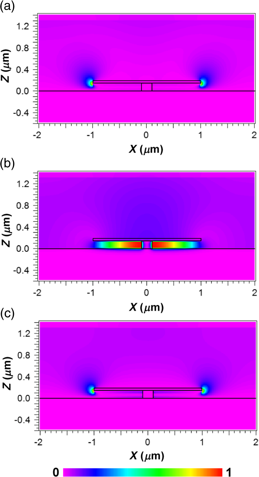
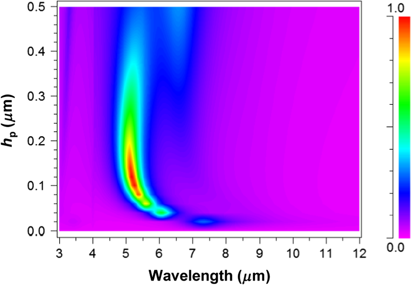
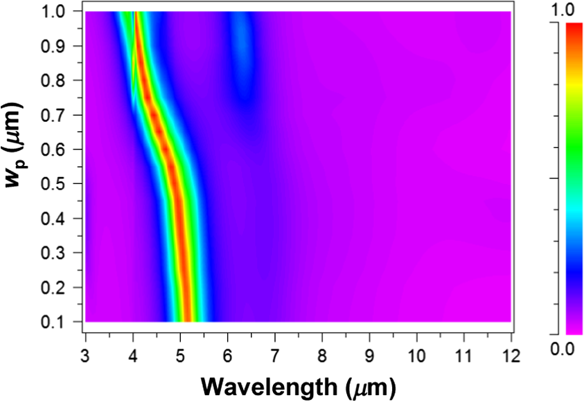
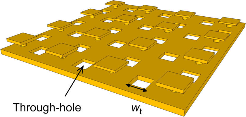
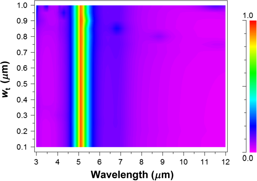
1.IntroductionThere has been increasing interest in uncooled infrared (IR) sensors with a microelectromechanical system-based pixel structure due to their low-cost fabrication and wide range of applications.1,2 We have recently developed uncooled IR sensors with advanced functions using plasmonics3,4 and metamaterials5,6 to expand their field of applications, which includes fire detection, gas analysis, hazardous material recognition, multicolor imaging, and polarimetric imaging. First, a wavelength-selective uncooled IR sensor was developed for the middle-wavelength infrared (MWIR) and long-wavelength infrared (LWIR) regions using a two-dimensional plasmonic absorber (2-D PLA).7–10 A 2-D PLA is an Au-based periodic dimple structure, in which surface plasmon resonance is produced and strong wavelength-selective absorption occurs according to the surface periodicity. A polarization-selective uncooled IR sensor was then developed using a 2-D PLA with ellipsoidal dimples11 and one-dimensional grating absorbers,12 whereby polarization could be selectively detected according to the asymmetry on the surface of the absorbers. Some advantages of 2-D PLAs are a simple fabrication procedure and structural robustness. Wavelength- and polarization-selective functions can be realized for PLAs without the attachment of filters,13 multilayer structures,14 mirrors,15 or polarizers,16,17 which effectively reduces the cost and additional space requirements of optical systems. Multicolor/polarimetric imaging can, therefore, be realized by the integration of various 2-D PLAs with different wavelength/polarization-detection specifications. 2-D PLAs inevitably require a large number of periods and a large thickness, which results in a large pixel size and a high-thermal mass.7,8 However, high-performance wavelength-selective uncooled IR sensors for multicolor IR imaging require a small pixel size and low-thermal mass to achieve high resolution and fast response. Metal-insulator-metal structures18–21 based on plasmonic metamaterials are important candidates for high-performance absorbers, which control the absorption wavelength according to the surface resonator size beyond the surface array period. However, insulator layers such as and SiN cause an additional absorption peak, restrict the operation wavelength to near the MWIR region due to their intrinsic absorption,22 and also increase the thermal mass. Therefore, we have proposed three-dimensional (3-D) or mushroom plasmonic metamaterial absorbers (MPMAs),23 as well as a suitable fabrication method.24 MPMAs with Si posts were also developed for dual- and single-band detection.25 However, MPMAs with Si posts require precise control of the post width to achieve single-mode operation. Therefore, we have investigated the detailed absorption properties of MPMAs based on all-metal structures to realize high-performance wavelength-selective uncooled IR sensors with wideband and single-mode operation. In this study, we report a theoretical investigation of MPMAs for high-performance uncooled IR sensors with advanced functions. 2.Absorption Wavelength Control2.1.Effect of the Micropatch ShapeFigure 1 shows schematic illustrations of the structure investigated in this study. The micropatches are arrayed and connected to the bottom plate with posts. This structure is referred to as a mushroom metamaterial.26,27 In this work, all of the components were assumed to be made of Au. The dielectric constant of Au used in our calculations was taken from Ref. 28. The minimum thickness of all components is approximately twice the skin depth to prevent light penetration and achieve ultrathin absorbers with low-thermal mass. The structural parameters of the period, the width (diameter) and thickness of the micropatch, the thickness of the bottom plate, and the width (diameter) and height of the posts are defined as , ; , ; ; and , respectively. The gap between the micropatches and the bottom plate is equal to . The thickness has no impact on the absorption, as long as it is sufficiently thick to reflect incident IR radiation. Thus, is considered to be at least in the IR wavelength region for practical applications29 and was set as a semi-infinite thickness for the simulation. The parameters , , and were fixed at 50, 200, and 150 nm, respectively. The incident angle is set to normal incidence for the fundamental evaluation of MPMAs conducted in this study. The polarization direction used is defined as that parallel to the basic lattice vector of the square lattice structure, which corresponds to the - and -directions, as shown in Fig. 1(b). The results obtained represent the averaged total absorption for all polarizations due to the symmetry of the MPMAs. Fig. 1Schematic illustrations of the mushroom plasmonic metamaterial absorber (MPMA) proposed in this study: (a) surface view and (b) cross-section of one unit cell with the incident light and the electric field directions are shown. 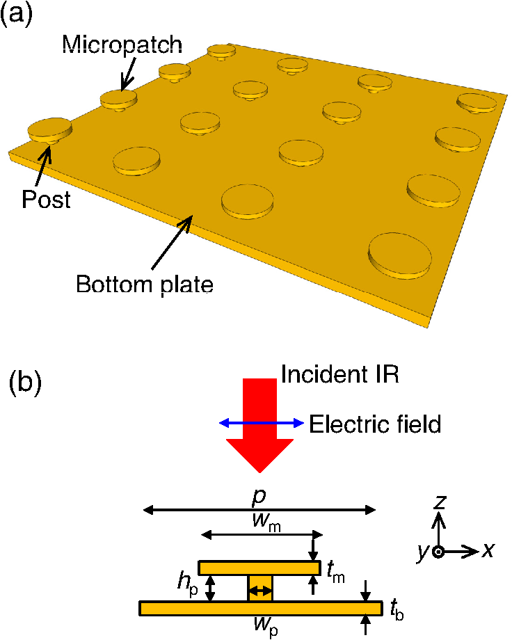 We first investigated the absorption properties of a circular-shaped micropatch using rigorous coupled-wave analysis (RCWA). The period was fixed at and was varied. Figures 2(a) and 2(b) show the absorption for the MPMAs with at 2.0, 2.5, 3.0, and , and the absorption for from 1.0 to as a function of the wavelength. Figure 2 indicates that sufficient absorption of over 90% was obtained for the MPMAs with most of the values, and the absorption wavelength could be controlled primarily by , regardless of . The absorption wavelength is almost proportional to ; however, a forbidden band where the absorption is suppressed appears for some values, such as 1.8, 2.5, 2.8, and . The full width at half maximum (FWHM) also increases with . As the absorption wavelength approaches the period, the FWHM is improved due to the reduction of the gap resonance between the micropatches. Fig. 2Calculated absorption spectra for the MPMA with circular-shaped micropatches. (a) Spectra for , 2.5, 3.0, and , and (b) spectra as a function of wavelength and . The colormap on the right side defines the absorption scale.  The absorption properties of square-shaped micropatches were also investigated by RCWA; a schematic illustration of an MPMA with square-shaped micropatches is provided in Fig. 3. As with the circular-shaped micropatch, the period was again fixed at and was varied. Figure 4 shows the wavelength absorption for this MPMA for various values of from 1.0 to . Sufficient absorption of over 90% was obtained for the MPMA with all of the values, and the absorption wavelength could be controlled according to , regardless of . The absorption wavelength is almost proportional to , and a uniform absorption peak is maintained over a wide range of MWIR and LWIR wavelengths compared with that for the MPMA with circular-shaped micropatches. Each circular-shaped micropatch forms an unequal gap with the adjacent micropatches, which produces broader resonance. In contrast, the square-shaped micropatches maintain a parallel gap with the adjacent micropatches, which produces narrower resonance. When the absorption wavelength is smaller than , diffraction starts to occur for both the circular- and square-shaped micropatches. Therefore, the absorption abruptly decreases for wavelengths . Fig. 3Schematic illustration of an MPMA with square-shaped micropatches. (a) Surface view and (b) cross-section of one unit cell with the incident light and the electric field directions are shown. 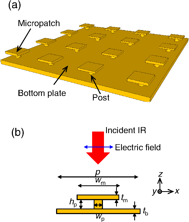 Fig. 4Calculated absorption spectra for the MPMA with square-shaped micropatches. (a) Spectra for , 2.5, 3.0, and , and (b) spectra as a function of wavelength and . 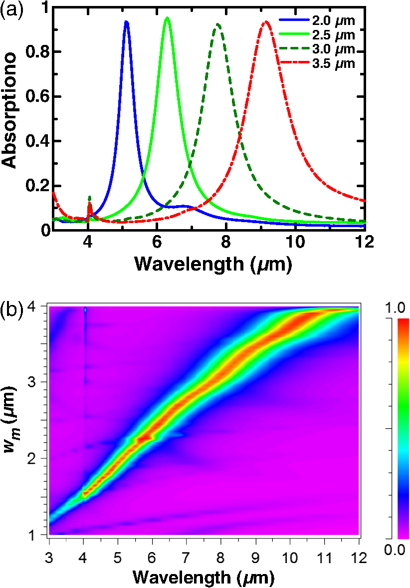 The time-averaged electromagnetic field amplitude distribution was calculated at the resonance using the 2-D finite-difference time-domain (FDTD) method. Here, was fixed at , whereas the values of the other parameters were the same as in the RCWA calculation. Figures 5(a)–5(c) show the normalized amplitude of the electric field and the magnetic field distribution, and the power, respectively. , , and are defined as parallel to , vertical to the -direction, and parallel to , respectively. Figure 5 clearly demonstrates that plasmonic resonance occurs only at the perimeter of the micropatch. These results confirm that localized plasmonic resonance rather than propagating plasmonic resonance occurs in the MPMAs. The absorption wavelength is defined only by the size of the micropatch beyond the pattern period due to this strong confinement of such localized plasmonic resonance, and thus contributes to a smaller pixel size. 2.2.Effect of the Post HeightThe effect of was investigated for an MPMA with square-shaped micropatches. Figure 6 shows the wavelength absorption for the MPMA as a function of from 0 to 500 nm with a fixed and of 2.0 and , respectively. Sufficient absorption of over 90% was obtained for ranging from to 200 nm, where the shift of the absorption wavelength was small. This result indicates that the narrow-gap resonance between the micropatches and the bottom plate is especially important to obtain sufficient absorption. 2.3.Effect of the Post WidthThe effect of was also investigated for an MPMA with square-shaped micropatches. Figure 7 shows the wavelength absorption for the MPMA as a function of from 100 nm to with a fixed and of 2.0 and , respectively. Sufficient absorption of over 90% was obtained, and a single absorption mode was achieved over a wide range of values from 100 nm to , which is half that of at . This result is attributed to the strongly localized plasmonic resonance at the edge of the micropatches. The post width has less impact on the absorption properties, and single-mode operation can be maintained, in contrast to the 2-D PLA with Si-post structures, which produces a gap resonant mode inside the Si post. 3.Effect of Through-HolesHigh-performance uncooled IR sensors require a small absorber volume to achieve fast responsivity. Through-holes are thus typically formed on absorbers to reduce the thermal mass. They are also beneficial for etchant or etching gas to fabricate thermal isolation structures by bulk micromachining. Therefore, the use of through-holes with the MPMA was investigated; Figure 8 shows a schematic illustration of the MPMA with square-shaped through-holes. The absorption properties of an MPMA with square-shaped micropatches and square-shaped through-holes were calculated by RCWA, in which and were fixed at 4.0 and , respectively. Figure 9 shows the wavelength absorption of the MPMA as a function of the through-hole width () from 100 nm to . The presence of through-holes had no influence on the absorption properties of the MPMA in the studied range. This indicates that the micropatches induced an antenna effect, because the plasmonic resonance mainly occurs at the edge of the micropatch, and narrow-gap resonance is formed, as shown in Fig. 5. The same effect was also confirmed for an MPMA with circular micropatches and circular through-holes. The through-holes did significantly reduce the absorber volume of the pixels, which leads to fast response and provides an advantage for surface micromachining techniques, such as under etching of the absorber area.30 4.ConclusionsAu-based MPMAs were theoretically investigated to aid the development of high-performance wavelength-selective uncooled IR sensors. The RCWA calculations demonstrated that wavelength-selective absorption could be realized depending on the shape and size of the micropatches. Broadband absorption was achieved with circular micropatches, whereas unity absorption was realized with square-shaped micropatches over a wide range of MWIR and LWIR wavelengths. The FDTD calculation demonstrated that the strong plasmonic resonance was confined at the edges of the micropatches, which leads to a small pixel size. A post height of to 200 nm was appropriate to obtain a narrow-gap resonance. However, the post width has less impact on the absorption properties and can maintain single-mode absorption, in contrast to that of Si-post structures. Through-holes can be formed on the bottom plate due to this 3-D plasmonic resonance and can reduce the thermal mass of the pixel as well as providing advantages for the fabrication of cavities. All-metal-based MPMAs can be applied for any type of uncooled IR sensors, such as thermopiles, bolometers, and silicon-on-insulator diodes.31,32 The results obtained here will contribute to the development of high-performance single-mode wavelength-selective uncooled IR sensors for multicolor imaging in the wideband MWIR and LWIR regions. AcknowledgmentsThe authors thank Masashi Ueno and Tetsuya Satake of the Advanced Technology R&D Center of Mitsubishi Electric Corporation for their helpful assistance. ReferencesP. W. Kruse, Uncooled Thermal Imaging Arrays, Systems, and Applications, SPIE Press, Bellingham, WA
(2001). Google Scholar
M. Kimata,
“Trends in small-format infrared array sensors,”
in Proc. Sensors,
1
(2013). Google Scholar
R. Stanley,
“Plasmonics in the mid-infrared,”
Nat. Photonics, 6
(7), 409
(2012). http://dx.doi.org/10.1038/nphoton.2012.161 NPAHBY 1749-4885 Google Scholar
S. Kawata,
“Plasmonics: future outlook,”
Jpn. J. Appl. Phys., 52
(1), 010001
(2013). http://dx.doi.org/10.7567/JJAP.52.010001 Google Scholar
D. R. Smith, J. B. Pendry and M. C. Wiltshire,
“Metamaterials and negative refractive index,”
Science, 305
(5685), 788
(2004). http://dx.doi.org/10.1126/science.1096796 SCIEAS 0036-8075 Google Scholar
T. Tanaka,
“Plasmonic metamaterials,”
IEICE Electron. Express, 9
(2), 34
(2012). http://dx.doi.org/10.1587/elex.9.34 Google Scholar
S. Ogawa et al.,
“Wavelength selective uncooled infrared sensor by plasmonics,”
Appl. Phys. Lett., 100
(2), 021111
(2012). http://dx.doi.org/10.1063/1.3673856 APPLAB 0003-6951 Google Scholar
S. Ogawa et al.,
“Wavelength selective wideband uncooled infrared sensor using a two-dimensional plasmonic absorber,”
Opt. Eng., 52
(12), 127104
(2013). http://dx.doi.org/10.1117/1.OE.52.12.127104 Google Scholar
K. Masuda et al.,
“Optimization of two-dimensional plasmonic absorbers based on a metamaterial and cylindrical cavity model approach for high-responsivity wavelength-selective uncooled infrared sensors,”
Sens. Mater., 26
(4), 215
(2014). SENMER 0914-4935 Google Scholar
Y. Takagawa, S. Ogawa and M. Kimata,
“Detection wavelength control of uncooled infrared sensors by two-dimensional lattice plasmonic absorbers,”
Sensors, 15
(6), 13660
(2015). http://dx.doi.org/10.3390/s150613660 SNSRES 0746-9462 Google Scholar
S. Ogawa et al.,
“Polarization-selective uncooled infrared sensor with asymmetric two-dimensional plasmonic absorber,”
Opt. Eng., 53
(10), 107110
(2014). http://dx.doi.org/10.1117/1.OE.53.10.107110 Google Scholar
S. Ogawa, Y. Takagawa and M. Kimata,
“Polarization-selective uncooled infrared sensor using a one-dimensional plasmonic grating absorber,”
Proc. SPIE, 9451 94511K
(2015). http://dx.doi.org/10.1117/12.2176549 PSISDG 0277-786X Google Scholar
Y. Ohtera and H. Yamada,
“Photonic crystals for the application to spectrometers and wavelength filters,”
IEICE Electron. Express, 10
(8), 20132001
(2013). http://dx.doi.org/10.1587/elex.10.20132001 Google Scholar
S. W. Han et al.,
“Design of infrared wavelength-selective microbolometers using planar multimode detectors,”
Electron. Lett., 40
(22), 1410
(2004). http://dx.doi.org/10.1049/el:20046547 Google Scholar
R. P. Shea, A. S. Gawarikar and J. J. Talghader,
“Midwave thermal infrared detection using semiconductor selective absorption,”
Opt. Express, 18
(22), 22833
(2010). http://dx.doi.org/10.1364/OE.18.022833 OPEXFF 1094-4087 Google Scholar
R. Haïdar et al.,
“Free-standing subwavelength metallic gratings for snapshot multispectral imaging,”
Appl. Phys. Lett., 96
(22), 221104
(2010). http://dx.doi.org/10.1063/1.3442487 APPLAB 0003-6951 Google Scholar
G. W. Kamerman et al.,
“Polarization state imaging in long-wave infrared for object detection,”
Proc. SPIE, 8897 88970R
(2013). http://dx.doi.org/10.1117/12.2028858 PSISDG 0277-786X Google Scholar
J. Hao et al.,
“High performance optical absorber based on a plasmonic metamaterial,”
Appl. Phys. Lett., 96
(25), 251104
(2010). http://dx.doi.org/10.1063/1.3442904 APPLAB 0003-6951 Google Scholar
T. Maier and H. Brueckl,
“Multispectral microbolometers for the midinfrared,”
Opt. Lett., 35
(22), 3766
(2010). http://dx.doi.org/10.1364/OL.35.003766 OPLEDP 0146-9592 Google Scholar
C. M. Watts, X. Liu and W. J. Padilla,
“Metamaterial electromagnetic wave absorbers,”
Adv. Mater., 24
(23), OP98
(2012). http://dx.doi.org/10.1002/adma.201200674 ADVMEW 0935-9648 Google Scholar
R. Feng et al.,
“Dual-band infrared perfect absorber based on asymmetric T-shaped plasmonic array,”
Opt. Express, 22
(S2), A335
(2014). http://dx.doi.org/10.1364/OE.22.00A335 OPEXFF 1094-4087 Google Scholar
Y. B. Chen and F. C. Chiu,
“Trapping mid-infrared rays in a lossy film with the Berreman mode, epsilon near zero mode, and magnetic polaritons,”
Opt. Express, 21
(18), 20771
(2013). http://dx.doi.org/10.1364/OE.21.020771 OPEXFF 1094-4087 Google Scholar
S. Ogawa et al.,
“Three-dimensional plasmonic metamaterial absorbers for high-performance wavelength selective uncooled infrared sensors,”
Proc. SPIE, 9070 90701Y
(2014). http://dx.doi.org/10.1117/12.2049895 PSISDG 0277-786X Google Scholar
S. Ogawa, D. Fujisawa and M. Kimata,
“Three-dimensional plasmonic metamaterial absorbers based on all-metal structures,”
Proc. SPIE, 9451 94511K
(2015). http://dx.doi.org/10.1117/12.2176550 PSISDG 0277-786X Google Scholar
S. Ogawa et al.,
“Mushroom plasmonic metamaterial infrared absorbers,”
Appl. Phys. Lett., 106
(4), 041105
(2015). http://dx.doi.org/10.1063/1.4906860 APPLAB 0003-6951 Google Scholar
D. Sievenpiper et al.,
“High-impedance electromagnetic surfaces with a forbidden frequency band,”
IEEE Trans. Microwave Theory Tech., 47
(11), 2059
(1999). http://dx.doi.org/10.1109/22.798001 IETMAB 0018-9480 Google Scholar
C. S. R. Kaipa, A. B. Yakovlev and M. G. Silveirinha,
“Characterization of negative refraction with multilayered mushroom-type metamaterials at microwaves,”
J. Appl. Phys., 109
(4), 044901
(2011). http://dx.doi.org/10.1063/1.3549129 JAPIAU 0021-8979 Google Scholar
A. D. Rakic et al.,
“Optical properties of metallic films for vertical-cavity optoelectronic devices,”
Appl. Opt., 37
(22), 5271
(1998). http://dx.doi.org/10.1364/AO.37.005271 APOPAI 0003-6935 Google Scholar
F. Neubrech et al.,
“Properties of gold nanoantennas in the infrared,”
Electronics and Photonics, 210 World Scientific Publishing Co., Singapore
(2008). Google Scholar
D. Fujisawa et al.,
“Multi-color imaging with silicon-on-insulator diode uncooled infrared focal plane array using through-hole plasmonic metamaterial absorbers,”
in Proc. MEMS,
905
–908
(2015). Google Scholar
D. Fujisawa et al.,
“Two-million-pixel SOI diode uncooled IRFPA with pixel pitch,”
Proc. SPIE, 8353 83531G
(2012). http://dx.doi.org/10.1117/12.919520 PSISDG 0277-786X Google Scholar
T. Maegawa et al.,
“2-in-1 diodes with a contact-sidewall structure for small pixel pitch in silicon-on-insulator (SOI) uncooled infrared (IR) focal plane arrays,”
Sens. Mater., 26
(4), 189
(2014). SENMER 0914-4935 Google Scholar
BiographyShinpei Ogawa received his BE, ME, and PhD degrees from the Department of Electronic Science and Engineering, Kyoto University, Japan, in 2000, 2002, and 2005, respectively. He has been with the Advanced Technology R&D Center, Mitsubishi Electric Corporation, Amagasaki, Japan, since 2005. He works on the development of various microelectromechanical system (MEMS) devices, including RF-MEMS switches, inductors, through-silicon via, optical sensors, and infrared (IR) sensors. He is currently a unit leader of plasmonics, metamaterials, and graphene research. Daisuke Fujisawa received his MS degree in electrical and electronic engineering in 2002 and his PhD in electronic and information engineering in 2005, all from Toyohashi University of Technology, Aichi, Japan. In 2005, he joined the Mitsubishi Electric Corporation, where he has been working at the Advanced Technology R&D Center. He currently works on the research and development of silicon-based IR focal plane arrays. Masafumi Kimata received his MS degree from Nagoya University in 1976 and received his PhD from Osaka University in 1992. He joined Mitsubishi Electric Corporation in 1976 and retired from Mitsubishi Electric in 2004. He is currently a professor at Ristumeikai University, where he continues his research on MEMS-based uncooled IR focal plane arrays and type-II superlattice IR focal plane arrays. He is a fellow of SPIE. |