|
|
1.IntroductionThe peak power handling capability of ultrashort pulse lasers is main concern for new facilities, like those for “Apollon 10P”1,2 and “extreme light infrastructure” pillars.3 Indeed, these last generation lasers require large () and resistant optical components with optimized thin-films coatings particularly to steer multi-petawatt (PW) beams at the output of the laser chain. In this context, the work related in this paper deals with the development and realization of large spectral bandwidth, high laser-damage threshold, and large-scale mirrors for such applications. Since the development of coating technologies for high-energy nanosecond laser lines like the laser mégajoule4 and the National Ignition Facility,5 most of the high-reflective optics steering high-fluence beams are designed from hafnia () and silica () stacks.6 In fact, deposition process has been fully improved in order to increase the laser resistance to reach the requirements for nanosecond near-infrared (IR) pulses.7,8 In the femtosecond regime, damage initiation is the results of nonlinear ionization processes, and the intrinsic laser resistance mainly depends on the bandgap of the material.9,10 With a bandgap of 5.5 eV, presents good qualities and this material is used in the design of high-reflective mirrors or other components for ultrashort optics. Alternatively, by mixing this material with silica, significant increase of the laser-damage threshold could be accomplished.11 We can note, however, that ion beam sputtering (IBS) or magnetron sputtering has been most studied for these applications. These last techniques are scalable to 1-m optics. However, electron-beam evaporation remains the main optical coating technology for large-scale laser optics. In the case of chirped pulse amplification, the extremely short pulse duration can only be achieved with broadband spectrum. In order to propagate these laser beams and also to manage the dispersion, another combination of materials, with higher refractive indices ratios than the couple, has to be used in the design to make the reflectivity band broad enough.12 Oliver et al.,13 for instance, have used a combination of alumina, hafnia, silica, niobia and metallic films to produce high-damage-threshold, broadband coatings for 15-fs pulses. High-reflection (HR) coatings with broad bandwidth have also been achieved by using a combination of hafnia, silica, and niobia.14 In this paper, we report on the characterization of electron-beam-deposited dielectrics, namely, , , , , , , and . We present the tests results of the intrinsic materials and the evolution of the laser-induced damage threshold (LIDT) with the increase of the number of pulses for different materials and deposition process parameters. We also study the electric field intensity (EFI) distribution inside the layers and discuss about the relationship between the LIDT of a multilayer dielectric and the LIDT of materials composing the stack. Eventually, results with optimized designs are presented. 2.Experiments2.1.FabricationFor this study, single layers of several dielectric materials and HR multilayers for S-polarization or P-polarization were deposited on fused silica substrates, cleaned with a specific procedure for laser applications. These substrates have the following specifications: fused silica 7980 (Corning), in diameter, and 5 mm in thickness, peak to valley wavefront error, Scracth/Dig:20/10. The samples were manufactured using electron-beam deposition and ion-assisted deposition (IAD) processes relevant for a 1-m class coating chamber. The chamber is a BAK1730 pumped with 2 cryogenic units (residual pressure ) and equipped with electron guns and an ion source. Both in-situ optical (visible and near IR) and quartz monitoring systems provide layer thickness control. The temperature is regulated, both on the front and rear side of substrates, within 1 K by pyrometric sighting. 2.2.CharacterizationsThe reflection and transmission spectra of the deposited layers were measured with a Perkin ELMER LAMBDA 950 UV/Vis/NIR Spectrophotometer. Then, fitting these curves using TFCalc™ software, we determined the refractive index dispersion of the materials and physical thickness. The electric field distributions in the samples were computed from the determined refractive index and thickness, with a self-developed code based on matrix formalism. The bandgap energies were deduced from the UV cut-off wavelength (50% transmission wavelength). The accuracy of this method is estimated around by comparison with other method, such as Tauc-Laurenz fit.15 Moreover, the absorption measurements were done with the photodeflection technique16 using a continuous-wave copper vapor laser. The 20-W and 511-nm beam is horizontally polarized and focus at the surface of the sample with 45-deg angle of incidence. The diameter of the irradiated area is . The reference used for the calibration of the signal is an aluminum mirror deposited on a fused silica substrate (), which reflective coefficient is known from a reflectometer measurements (0.2% accuracy). The calibration is validated by measuring a very low absorption () dielectric standard. The absolute accuracy of the absorption measurement is estimated around , whereas the relative accuracy, for measurement performed with the same calibration data, is about . The x-ray diffraction (XRD) measurements were done at “Institut Materiaux Microlectronique Nanoscience de Provence” (Im2np, Marseille) with a Philips X’Pert MPD X-Ray source (Cu and ) and a Panalytical X’Celerator fast collector. To measure the stress of the coating, a well-calibrated wedged sample is coated during film deposition. The reflective wavefront shape of the coated face of this specific sample is measured, before and after coating, with a Zygo Mark II interferometer at 633 nm in the Fizeau configuration. The average stress is then deduced from a differential analysis of the two measurements through a self-developed Zernike polynomial fitting algorithm. 2.3.Laser-Induced Damage Threshold MeasurementsLaser-induced damage measurements were performed on the experimental setup described by Mangote et al.15 For this work, the 1030-nm beam line was used at 10-Hz repetition rate with 500-fs pulses. Calibrations of the laser (temporal profile, energy extraction, and spatial profile) have been carried out before and after each test campaign of this study. The effective surface of the focused beam is in accordance to ISO 21254 and was ( diameter at ). The error budget of the absolute fluence determination is estimated to be less than , however, the relative fluence error in a test campaign can be measured with a better accuracy and was estimated to be for the present experiments. Some of the tests were conducted in vacuum environment and down to cryogenic temperatures in a dedicated cell. The configuration for these tests is schematically described in Fig. 1. A picture of the vacuum/cryo cell is also displayed. The cryogenic temperature cell consists of a vacuum jacket that contains a refrigerant dewar/cell assembly and a heating block that contains the sample. The whole assembly is operated within a vacuum environment, down to in this work. Using a combination of liquid nitrogen refrigerant and control from the cell block heaters, the temperature can be varied from to 250°C, from the manufacturer specifications. The external windows are also heated to prevent condensation and the heating block is operated by a separate high stability controller supplied with the system. The cell has two window ports made of UV-fused silica with wedged and uncoated faces; one is used for the laser beam entrance to irradiate the sample, and the other is used for backside observation, as described in Fig. 1. Fig. 1Picture and schematic of the cryogenic and vacuum cell and experimental configuration for the laser damage tests. 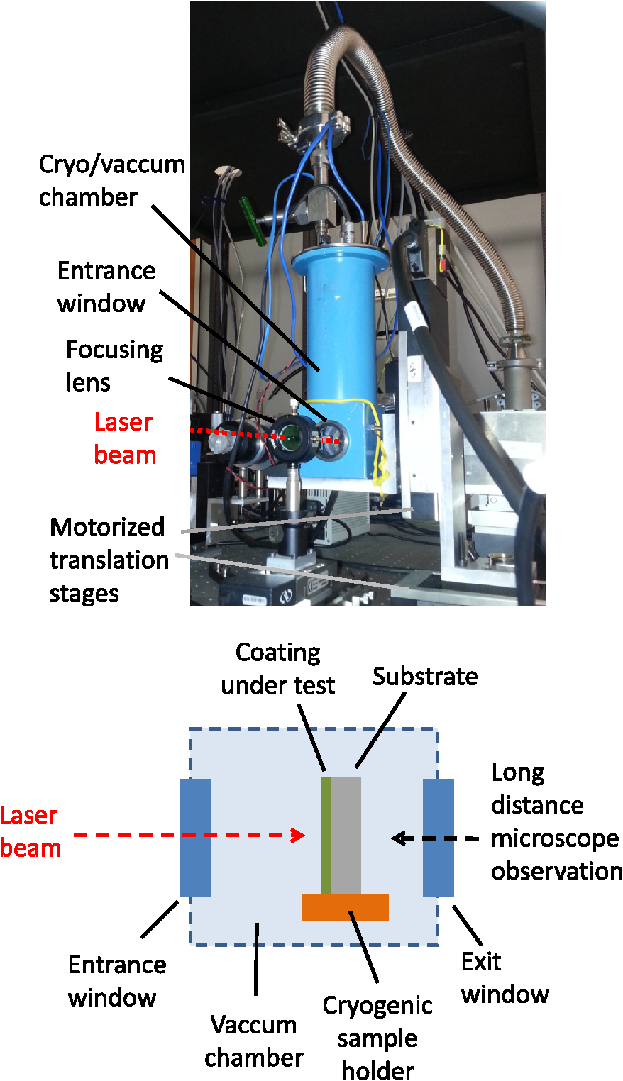 When the vacuum/cryo cell is used for the experiments, the laser beam is passing through the 3-mm thick fused silica window that is placed between the focusing lens and the sample to be tested, this sample being at from the window. In this configuration, self-focusing in the window could potentially affect the damage threshold measurement, by altering the position and size of the focal waist. Based on a nonlinear refractive index for fused silica of in the subpicosecond regime17 and the optical configuration, a phase shift estimated to 0.1 rad should occur after passing through this window, for a fluence on the sample of . The effect is therefore non-negligible and as it scales linearly with the intensity, it must be taken into consideration when analyzing the results: differences were observed between measurements made with and without this window. In order to discuss the data, we rescaled the data of each sample by a coefficient defined as the LIDT measured in atmospheric conditions inside the vacuum and cryogenic cell divided by the LIDT measured in the standard configuration. The samples were irradiated with the same parameters on 10 sites for each energy level in order to get statistical data. The steps between the energy level are set to be in the error bar of the energy measurement. The sites are irradiated with a single pulse (“1-on-1” mode) or multiple pulses (“S-on-1” mode). Measurements of single layer samples were done at 0 deg of incidence in ambient conditions or in the cryogenic/vacuum chamber, with a pressure of and temperatures ranging from to 50°C. HR coatings were tested in ambient conditions at 45 deg of incidence. Ex-situ damage inspection with a Nomarski/dark field microscope is performed afterward. An irradiated site is considered as damaged for any visible modification detected through this system. The LIDT is then defined as the mean between the lowest fluence with a nonzero probability damage and the the highest fluence with a zero probability damage. In the cases of material studies through single layers, the thresholds are corrected by the maximum of the EFI computed inside the layer for the value to be representative of the material without any interference contribution. 3.Results and Discussion3.1.HafniaHafnia is one of the most important high index materials for the production of optical multilayer coatings for UV to IR applications. In addition to its good optical and mechanical properties, it is known for its high LIDT: it has been shown through different studies that hafnia coatings with very high laser-damage threshold can be obtained in the nanosecond,6,18,19–22 picoseconds,9 and femtosecond9,23 regime. A special attention has then been paid to this material and we have investigated the influence of the deposition parameters on the laser-damage resistance of the material. Five single layers of hafnia were deposited on silica substrates with several process parameters, as described in Table 1. They have been analyzed with the different characterization tools described in the previous section. In Fig. 2, we present the transmittance and reflectance measurements obtained by spectrophotometry and the XRD spectrum of the samples showing their crystalline level. Depending on the deposition conditions, amorphous or polycrystalline phases are evidenced on the samples. The appearance of the polycrystalline phases is favored by a high temperature during the deposition process and can be detrimental for the homogeneity of the film’s properties by creating absorbing centers. The refractive index obtained from the spectrophotometric measurements is between 1.83 and 1.93 (Table 1). The estimated bandgaps are in the range 5.7 to 5.9 eV, as reported in Table 1. Because the laser-damage process in the femtosecond regime is the consequence of nonlinear ionization process, the bandgap value is a critical parameter that drives the laser-damage resistance, at least for single-pulse irradiation.9 The bandgap values are in the same range considering the error bar on the bandgap estimation. We can notice, however, a lower value for the IAD sample. The absorption level ranges between 20 and 60 ppm (), nevertheless a higher absorption level has been measured for the sample made with IAD, which is explained by the use of nonoptimized parameters and contamination during the process. Table 1Properties of HfO2 single layer samples. Ti corresponds to the temperature during sample i deposition process. Refractive index is given at 1030 nm. Absorption is given at 511 nm.
Fig. 2(a) Transmittance and reflectance curves used for the determination of the refractive index and band-gap energy of each layer. (b) XRD spectrum of the studied hafnia single layers showing their crystalline level. The reference corresponds to a powder measurement from the “International Centre for Diffraction Data.”  The results of the LIDT tests performed on the single layers are reported in Fig. 3. Considering the error bars on the measurements, the results do not reveal any significant difference between the samples. The LIDT for single pulse is around , which is in agreement with measurements on other samples on the same experiment, including IBS coatings.24 We observe a decrease of the LIDT with the number of applied pulses that corresponds to a drop of of the threshold in the first 100 pulses, as observed also in other works with similar irradiation conditions.25,26 This behavior was attributed to the high densities of deep and shallow traps, i.e., electronic states in the forbidden band that can trap the conduction band electrons after a subthreshold irradiation.27 Fig. 3LIDT measurement at 500 fs and 1030 nm, at normal incidence in the air of single layers deposited with different processes. (a) Comparison of the LIDT for different pulse numbers. (b) Observation of the determinism of the damage probability for each sample and each pulse number. 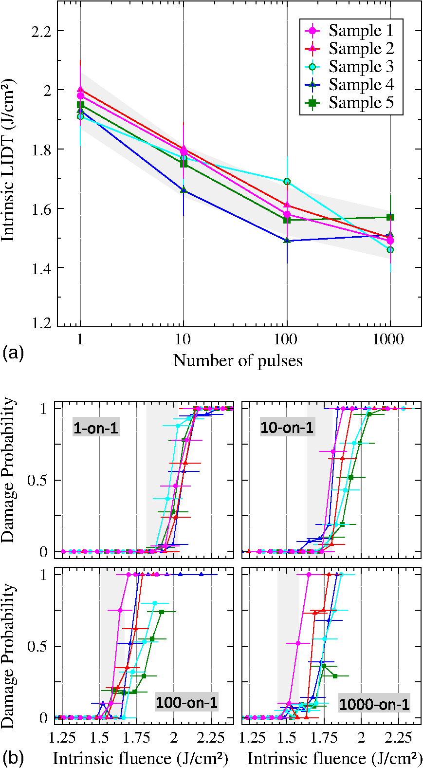 Therefore, we cannot correlate any process parameters or any physical properties of these hafnia layers to their intrinsic LIDT. Indeed, the choice of the source material (Hf or ) has no significant impact on the LIDT of the material, as well as the absorption level in the visible spectral range. In spite of that, it appears that there is a very low effect (just near the error bar) of the crystallinity of the material on the LIDT. For deposited from the metallic form, the crystalline structure had a lower LIDT than the amorphous structure but only for single pulse. For deposited from its oxidized form, the crystalline structure had a lower LIDT than the amorphous structure whatever the number of pulses. That confirms the material intrinsic nature importance during the interaction of the thin films with femtosecond pulses. However, regarding the determinism (the evolution of the slope between the 0% and 100% damage probabilities), we observe a possible link with the absorption level. In fact, the highest slope corresponds, for every pulse number up to 1, to the sample 1, which has the lowest absorption level. And the lower slope corresponds to sample 5 (-IAD), which has the highest absorption level. 3.2.Additional Dielectric Single LayersAs discussed in Sec. 1, other materials have to be combined to hafnia and silica to obtain a broadband mirror. In order to build a LIDT database to design multidielectric stacks, single layers of several dielectrics materials (, , , , , and ) were deposited on fused silica substrates. The optical thickness of each layer is a quarter wave at 800 nm. The properties of the layers, obtained with the characterization techniques presented before, are reported in Table 2. Table 2Properties of dielectric materials deposited as single layer onto silica substrates. Refractive index is given at 1030 nm and absorption is given at 511 nm.
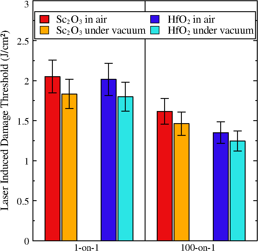
The results of the damage tests are reported in Fig. 4. The intrinsic LIDT is plotted as a function of the measured gap, since the main property that drives the laser-damage resistance is the optical bandgap, and as a function of the refractive index, which is the interesting material parameter for the design of multilayer optical components. Fig. 4(a) Intrinsic LIDT versus refractive index and (b) intrinsic LIDT versus bandgap energy and measurement performed in normal incidence at 500 fs and 1030 nm with “1-on-1” and “100-on-1” methods. 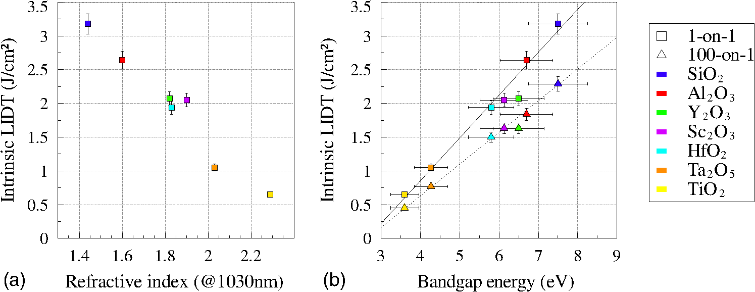 A linear dependency of the LIDT with respect to the bandgap value is observed, which is in agreement with other observations made on a large range of coating materials and manufacturing techniques.9,24 In the case of single pulses, the LIDT (in ) dependency with bandgap (in eV) can be fitted with the following equation: This equation corresponds also to the empirical description made by Gallais and Commandré24 for many materials deposited with various conditions. This linear behavior can be explained by taking into account the physical processes involved in the ionization processes at the initiation of the damage event (photo and impact ionization) and their dependency with the bandgap.9,10 The optical bandgap and refractive index are related to each other: the relationship between bandgap and refractive index has a linear behavior in the range of interest.24 As a consequence, the LIDT is linearly decreasing with the refractive index of the material, as observed in Fig. 4.A decrease of the LIDT is observed for all the tested materials after irradiation with 100 pulses. The threshold drops to around 20% to 25% of the initial single threshold. The “100-on-1” LIDT follows also a linear dependence on bandgap, as evidenced in Fig. 4. This “fatigue” or “incubation” behavior has been extensively studied26,28 and the physical mechanism is related to the accumulation of electronic defects in the materials. Therefore, there is no physical reason to obtain the same fatigue effect for all materials: by increasing the number of pulses, the LIDT should not be linearly dependent on the material bandgap anymore. The investigation was not conducted any further in the present study because the effect is strongly dependent on the irradiation conditions and should be studied in the conditions of the final application of the coatings, taking into account the pulse duration and repetition rate. 3.3.Environmental ConditionsOptical components for high power ultrashort lasers have to be operated in vacuum conditions in order to avoid nonlinear effects in the air. The effect of ambient pressure on the laser-damage resistance in the femtosecond regime has not been the subject of many reports in the literature. The main work on the subject was done by Nguyen et al.:29 the laser-damage threshold of metal oxide coatings was studied for different ambient gas pressures (oxygen, nitrogen, water vapor, toluene) down to with 50-fs pulses at 800 nm. They have shown that the single-pulse damage threshold is independent of the vacuum conditions, because it is related to intrinsic material properties, whereas the multipulse damage threshold is affected. The authors have suggested a mechanism based on an accumulation of oxygen vacancy defects in the material that increase the absorption level of the films. The observed effect is however dependent on pressure and should be dependent on irradiation conditions (number of pulses, pulse duration, and pulse frequency) because it is the case in the air. In the present experiments, the effect has been studied for 500-fs pulses under a pressure of () in the configuration described previously. The samples used for the experiments whose results are presented in this section are the same, as those presented in the previous part. Calibration and spot size measurements were done after the entrance window. The LIDT of the samples was determined first in air for comparison with tests done without the vacuum chamber in order to evidence any possible artifacts related to nonlinear effects in the entrance window, and second, the test was repeated after reaching the base pressure. The tests were done with “1-on-1” and “100-on-1” modes. They are reported in Fig. 5. From these results, it is very difficult to conclude about any possible influence of ambient pressure in our test conditions: the observed 10% decrease is in the error bar of our measurements. For other tests, as the ones reported in Fig. 6, this decrease was not observed. We can note that in the work published by Nguyen et al., a 10% decrease of the LIDT under vacuum between “1-on-1” and “100-on-1” tests was observed but for lower pressures. Fig. 6Intrinsics LIDT of dielectrics materials under vacuum at different temperatures (horizontal lines correspond to the respective intrinsic LIDT in air at room temperature). The green line (respectively orange) shows the LIDT level for the case of ambient pressure for (respectively ) and the green (orange) area is the uncertainty area.  A temperature dependence of the LIDT of optical coatings under pulse irradiation has been recently reported by Mikami et al.:30 for pulses longer than a few picoseconds, the LIDT was observed to increase with decreasing temperature, whereas there was no temperature dependence or a slightly reversed tendency for pulses shorter than a few picoseconds. On a physical point of view, the authors suggest a temperature dependence of the avalanche process for the interpretation of the experimental observations. Our application does not require cryogenic environments, but we have tested the temperature dependence of the single-pulse LIDT for the and samples, in order to see if the LIDT could be improved. The tests were done in vacuum, in the conditions described above. The LIDT of the sample was measured in air, then in vacuum, and then in vacuum at . The sample was then heated and stabilized to higher setpoint temperatures and the LIDT measured again up to . The results of the LIDT measurements are shown in Fig. 6. As evidenced in Fig. 6, there is no dependence of the LIDT with temperature at 500 fs, at least for the case of single-pulse irradiation. These results are in good agreement with the report of Mikami et al. (that were done for 15 pulses irradiation), where no dependence was observed for 2-ps pulses and a weak dependence for 100-fs pulses. 3.4.StacksThe previous sections were dealing with the laser-damage resistance of single layer coatings. Based on these results, specific components can be designed and the laser-damage resistance should be predicted if the films are manufactured using the same deposition conditions, based on the following equation:31 where is the intrinsic laser-damage threshold of the materials in the stack, is the incident EFI, and is the maximum EFI in each of the materials.This is a commonly used approach based on the fact that LIDT depends on the intensity level in the material and on the assumption that the behavior of the material is the same if it is deposited as a single layer or embedded in a stack. However, even if there have been investigations on the correlation between the peak field and LIDT,32,33 there is no clear experimental demonstration in the literature of this approach. Therefore, specific experiments were conducted to assess experimentally that the theoretical LIDT prediction of a given stack can be obtained from the knowledge of its electric field distribution and intrinsic LIDT of materials forming the stack. Several 45-deg broadband high-reflective coatings were designed from the dielectric materials described in the previous part and manufactured using the same deposition conditions. The stacks were not specifically designed for high laser-damage resistance but only for the broad band, the high reflectivity, and the test laser wavelength. Different designs, different number of pulses, and different polarizations were used to have a distribution of theoretical LIDT. The results of the damage tests on these samples are reported in Fig. 7. The results are plotted with the predicted LIDT from Eq. (2) as the vertical axis and the measured LIDT as the horizontal axis. We recall that the “predicted” LIDT corresponds to the expected resistance based on LIDT measurement of single layer and E-field distribution in the stack. The white area on the figure corresponds to the part where the expected and experimental values are the same, considering the error bars on the measurements. A conservative 20% error bar was taken: 10% for LIDT determination and 10% for electric field calculations based on refractive index and thicknesses. Obviously, there is a clear evidence of the validity of the approach. Fig. 7(a) Predicted LIDT from Eq. (2) versus experimental LIDT of 45-deg broadband HR-coatings. (b) Reflectivity spectra of most resistant design in P- and S-polarization. 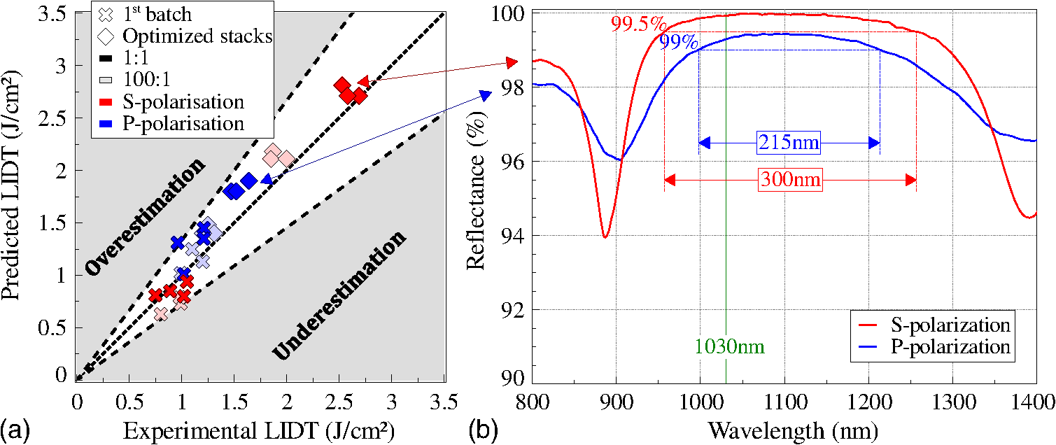 Based on this validation of the approach, a second set of samples was manufactured with optimized designs for a high LIDT and a broadband reflection spectrum. The results of the LIDT tests are given also in Fig. 7, as the reflectivity spectrum of the more-resistant design for each polarization, showing that broadband high laser-damage threshold mirrors can be achieved. Let us note that higher damage threshold can be obtained at the cost of a reduction of the width of the HR spectral range. 4.ConclusionThe laser-damage resistance of different dielectric materials of interest for high-power femtosecond applications, and deposited with electron-beam processes, was investigated at 500 fs, 1030 nm. The damage thresholds of the materials were found to be linearly dependent on bandgap, as evidenced in previous studies, and we have not found a strong dependency with the deposition parameters. Ambient pressure (down to ) and temperature (down to ) were not found to influence the laser-damage resistance of the materials. Based on an experimental approach that has involved many different single layers and multilayer stacks, we are able to demonstrate the validity of designing high laser-damage resistant multilayer stacks for ultrashort applications based on EFI calculation and the knowledge of the single layers’ LIDT. This approach has been used to produce high reflective, broadband (300 nm), and high laser-damage threshold () for femtosecond applications. The scaling of these results for shorter pulse durations was not reported in this paper but was validated and should be the subject of another detailed publication. As we exclusively worked with materials compatible with meter class processes, this study gave us with the ability to coated large optical components, to be integrated in multi-PW laser system, like folding mirrors, deformable mirrors and 90-deg off-axis parabola. As an example, we report in Fig. 8 on the production of an ultrabroad band high reflector off-axis parabola based on the work presented in this paper (correspond to the best sample of Fig. 7). Due to this study, the mirrors for the Appolon 10PW laser project have been defined and manufactured (they correspond to the design of samples of Fig. 7) and they are being installed. Fig. 8Picture of 90-deg off-axis parabola with a high laser resistance coating for multi-PW laser systems. 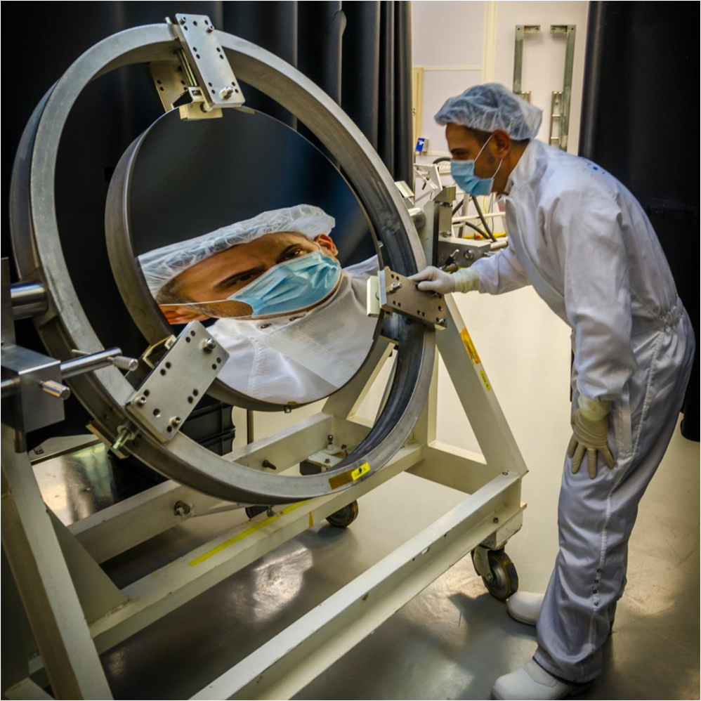 We should note that in this work, we have investigated and optimized the intrinsic laser-damage resistance of the stacks. However, macroscopic defects related to the deposition conditions can have an impact of the laser-damage resistance,34 particularly, for large optics. They were not investigated in these experiments but they are a main concern and should be the subject of future investigations. ReferencesG. Chériaux et al.,
“Apollon-10P: status and implementation,”
in Proc. AIP,
78
(2012). Google Scholar
D. Papadopoulos et al.,
“The Apollon-10P project: design and current status,”
in Advanced Solid-State Lasers Congress, OSA Technical Digest,
(2013). Google Scholar
M. L. Andre,
“Status of the LMJ project,”
Proc. SPIE, 3047 38
(1997). http://dx.doi.org/10.1117/12.294307 PSISDG 0277-786X Google Scholar
G. H. Miller, E. I. Moses and C. R. Wuest,
“The national ignition facility,”
Opt. Eng., 43 2841
–2853
(2004). http://dx.doi.org/10.1117/1.1814767 Google Scholar
C. J. Stolz, M. D. Thomas and A. J. Griffin,
“BDS thin film damage competition,”
Proc. SPIE, 7132 71320C
(2008). http://dx.doi.org/10.1117/12.806287 PSISDG 0277-786X Google Scholar
B. Pinot, H. Leplan and F. Houbre,
“Laser Mégajoule 1.06 μm mirrors production, with very high laser damage threshold,”
Proc. SPIE, 4679 234
(2002). http://dx.doi.org/10.1117/12.461687 PSISDG 0277-786X Google Scholar
J. B. Oliver,
“Evaporated HfO2 / SiO2 Optical coatings and modifications for high-power laser applications,”
(2012). Google Scholar
M. Mero et al.,
“Scaling laws of femtosecond laser pulse induced breakdown in oxide films,”
Phys. Rev. B, 71 115109
(2005). http://dx.doi.org/10.1103/PhysRevB.71.115109 Google Scholar
B. Mangote et al.,
“Femtosecond laser damage resistance of oxide and mixture oxide optical coatings,”
Opt. Lett., 37 1478
(2012). http://dx.doi.org/10.1364/OL.37.001478 OPLEDP 0146-9592 Google Scholar
M. Jupé et al.,
“Improvement in laser irradiation resistance of fs- dielectric optics using silica mixtures,”
Proc. SPIE, 6403 64031A
(2007). http://dx.doi.org/10.1117/12.696131 PSISDG 0277-786X Google Scholar
H. A. Macleod, Thin-Film Optical Filters, 4th ed.Taylor & Francis, Boca Raton
(2010). Google Scholar
J. B. Oliver et al.,
“Reactive ion-assisted deposition of e-beam evaporated titanium for high refractive index TiO2 layers and laser damage resistant, broad bandwidth, high-reflection coatings,”
Appl. Opt., 53 A205
(2014). http://dx.doi.org/10.1364/AO.53.00A221 APOPAI 0003-6935 Google Scholar
J. Bellum et al.,
“Plasma-ion-assisted coatings for 15 femtosecond laser systems,”
Appl. Opt., 53 A205
(2014). http://dx.doi.org/10.1364/AO.53.00A205 APOPAI 0003-6935 Google Scholar
B. Mangote et al.,
“A high accuracy femto-/picosecond laser damage test facility dedicated to the study of optical thin films,”
Rev. Sci. Instrum., 83 013109
(2012). http://dx.doi.org/10.1063/1.3677324 RSINAK 0034-6748 Google Scholar
W. B. Jackson et al.,
“Photothermal deflection spectroscopy and detection,”
Appl. Opt., 20 1333
(1981). http://dx.doi.org/10.1364/AO.20.001333 APOPAI 0003-6935 Google Scholar
S. Santran et al.,
“Precise and absolute measurements of the complex third-order optical susceptibility,”
J. Opt. Soc. Am. B, 21 2180
(2004). http://dx.doi.org/10.1364/JOSAB.21.002180 JOBPDE 0740-3224 Google Scholar
R. Chow et al.,
“Reactive evaporation of low defect density hafnia,”
Appl. Opt., 32 5567
(1993). http://dx.doi.org/10.1364/AO.32.005567 APOPAI 0003-6935 Google Scholar
P. André, L. Poupinet and G. Ravel,
“Evaporation and ion assisted deposition of HfO2 coatings: some key points for high power applications,”
J. Vac. Sci. Technol., 18 2372
(2000). http://dx.doi.org/10.1116/1.1287153 JVSTAL 0022-5355 Google Scholar
M. Alvisi et al.,
“HfO2 films with high laser damage threshold,”
Thin Solid Films, 358 250
–258
(2000). http://dx.doi.org/10.1016/S0040-6090(99)00690-2 THSFAP 0040-6090 Google Scholar
D. Zhang et al.,
“High laser-induced damage threshold HfO2 films prepared by ion-assisted electron beam evaporation,”
Appl. Surf. Sci., 243 232
–237
(2005). http://dx.doi.org/10.1016/j.apsusc.2004.09.083 ASUSEE 0169-4332 Google Scholar
J. B. Oliver et al.,
“Optimization of laser-damage resistance of evaporated hafnia films at 351 nm,”
Proc. SPIE, 7132 71320J
(2009). http://dx.doi.org/10.1117/12.805383 PSISDG 0277-786X Google Scholar
C. J. Stolz et al.,
“Thin film femtosecond laser damage competition,”
Proc. SPIE, 7504 75040S
(2009). http://dx.doi.org/10.1117/12.837473 PSISDG 0277-786X Google Scholar
L. Gallais and M. Commandré,
“Laser-induced damage thresholds of bulk and coating optical materials at 1030 nm, 500 fs,”
Appl. Opt., 53 A186
(2014). http://dx.doi.org/10.1364/AO.53.00A186 APOPAI 0003-6935 Google Scholar
D. N. Nguyen et al.,
“The effect of annealing on the subpicosecond breakdown behavior of hafnia films,”
Proc. SPIE, 7132 71320N
(2008). http://dx.doi.org/10.1117/12.804452 PSISDG 0277-786X Google Scholar
D. B. Douti, L. Gallais and M. Commandre,
“Laser-induced damage of optical thin films submitted to 343, 515, and 1030 nm multiple subpicosecond pulses,”
Opt. Eng., 53 122509
(2014). http://dx.doi.org/10.1117/1.OE.53.12.122509 Google Scholar
L. A. Emmert, M. Mero and W. Rudolph,
“Modeling the effect of native and laser-induced states on the dielectric breakdown of wide band gap optical materials by multiple subpicosecond laser pulses,”
J. Appl. Phys., 108 043523
(2010). http://dx.doi.org/10.1063/1.3457791 JAPIAU 0021-8979 Google Scholar
M. Mero et al.,
“On the damage behavior of dielectric films when illuminated with multiple femtosecond laser pulses,”
Opt. Eng., 44 051107
(2005). http://dx.doi.org/10.1117/1.1905343 Google Scholar
D. N. Nguyen et al.,
“Femtosecond pulse damage thresholds of dielectric coatings in vacuum,”
Opt. Express, 19 5690
(2011). http://dx.doi.org/10.1364/OE.19.005690 OPEXFF 1094-4087 Google Scholar
K. Mikami et al.,
“Temperature dependence of laser-induced damage threshold of optical coatings at different pulse widths,”
Opt. Express, 21 28719
(2013). http://dx.doi.org/10.1364/OE.21.028719 OPEXFF 1094-4087 Google Scholar
M. Jupe et al.,
“Mixed oxide coatings for advanced fs-laser applications,”
Proc. SPIE, 6720 67200U
(2007). http://dx.doi.org/10.1117/12.753730 PSISDG 0277-786X Google Scholar
K. Starke, T. Gross and D. Ristau,
“Laser-induced damage investigation in chirped mirrors for ultrashort-pulse laser systems,”
Proc. SPIE, 4347 528
(2001). http://dx.doi.org/10.1117/12.425058 PSISDG 0277-786X Google Scholar
G. Abromavicius et al.,
“Influence of electric field distribution on laser induced damage threshold and morphology of high reflectance optical coatings,”
Proc. SPIE, 6720 67200Y
(2007). http://dx.doi.org/10.1117/12.752902 PSISDG 0277-786X Google Scholar
L. Gallais, X. Chen and Z. Wang,
“Influence of nodular defects on the laser damage resistance of optical coatings in the femtosecond regime,”
Opt. Lett., 39 1545
(2014). http://dx.doi.org/10.1364/OL.39.001545 OPLEDP 0146-9592 Google Scholar
|