|
|
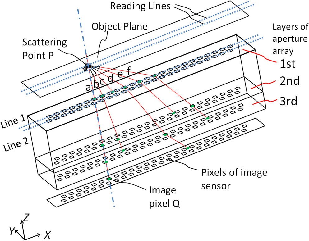
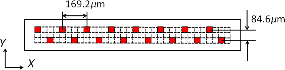
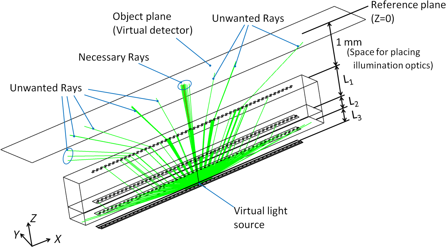
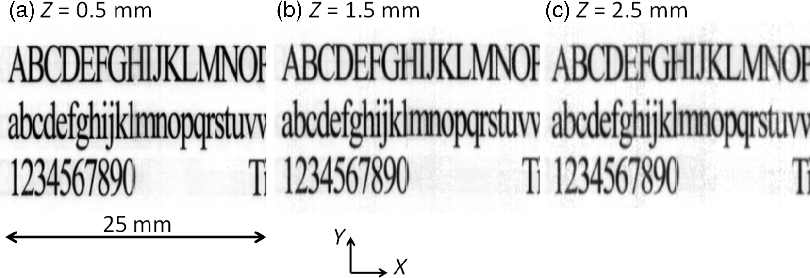
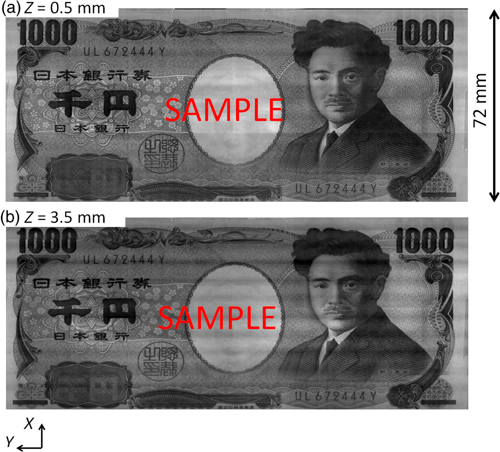
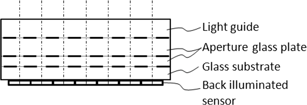
1.IntroductionLensless imaging has been studied, according to several different kinds of principles, since the early days of optical imaging. A pinhole camera is one of the simplest ways of creating an image but has the disadvantages of low resolution and low light efficiency. Coded aperture imaging has been studied in the field of astronomical observation by x-ray or gamma-ray, for which manufacturing an imaging lens is difficult, to improve the low light efficiency.1–3 Overlapped images through the coded pattern holes are reconstructed using a computer algorithm. Recently, application of coded aperture to photos in visible light has been reported.4 Variable coded aperture using a liquid crystal device has also been reported.5 A lensless miniature CMOS imager has been proposed, which uses a unique angle-sensitive pixel sensor and a spiral pattern grating.6 However, except for the simple pinhole camera, the above methods require a reconstruction process in computers, and the quality of images is less than that of a normal camera using collecting lenses or mirrors. A direct contact method was actively studied from the 1980s to the early 1990s for use of a scanner of a facsimile apparatus, in which a paper as an object is directly placed in contact with an image-sensor chip like a stamp, and scattering rays from a point on the object plane are directly detected by the sensor chip.7 However, this was replaced by a rod lens array method that uses gradient index8 because the direct contact method has some drawbacks: the sensor chip is breakable due to the direct contact, it is difficult to make space for illumination optics, and the depth of field is virtually zero. A fingerprint sensor using the direct contact method9 is commercially available, employing direct contact with no space of illumination. Light illuminates the outside of the measured area, the light transmitted through the finger tissue is scattered at the surface asperity, and the scattered light is directly detected at a two-dimensional image sensor placed in contact with the finger. However, this method is not suitable for a document scanner because documents are not always in contact with the sensor and do not have surface asperity. Recently, mobile document scanners have come on the market, requiring a thinner scanner than the rod-lens-array scanner for ease of transport. We have developed an imaging scanner with 600-dpi resolution whose depth of field is larger than that of the traditional rod lens array scanner, by using reflective mirror arrays.10,11 It is comparable in size to the traditional one. We apply the lensless direct contact method to make our scanner thinner. The depth of field, the worst drawback of the direct contact method, is improved by our original multi aperture-array-layers placed on a linear image sensor, where each hole in the array has one-to-one correspondence to each pixel of the image sensor. Since the object plane is displaced from the image sensor, this makes space to place illumination optics and avoids destruction of the image sensor. We show the basic idea of our lensless image scanner in the following section, explain the design, and then show the results of prototype test. 2.Principle of Optical StampImage information on the object plane is transferred to the image sensor like a stamp if a structure is placed on the image sensor and limits scattering rays from the object in such a way that each point on the object corresponds to one pixel of the image sensor. A tube array as in Fig. 1(a) achieves this, where each tube with an aperture on the object side is placed on each imaging sensor pixel. However, it is not easy to mass-produce such a structure on the micrometer scale. A simple aperture array as in Fig. 1(b) permits oblique launching rays from a point on the object to reach pixels not corresponding to the object point, causing ghost images. Although two-aperture layers as in Fig. 1(c) can decrease such stray rays, this is insufficient. Fig. 1Basic concepts of optical stamp image scanner: (a) shielding pipe array, (b) one-layered aperture array, (c) two-layered aperture array, and (d) two-layered aperture array with staggered arrangement in two lows. 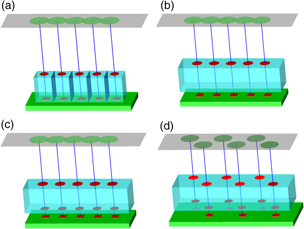 As shown in Figs. 1(d) and 2, we devise a new construction including the following two ideas: (a) staggered arrangement in two rows and (b) three aperture layers. The more aperture layers are stacked, the more rays transmitting obliquely inside the aperture layers can be shielded. Three aperture layers can be made by gluing two glass plates, both sides of which are masked in aperture patterns. The staggered arrangement as in Fig. 1(d) widens the pitch twice in one row in the direction, decreasing stray light paths inside the aperture layers. It maintains the same resolution because the images in the first row and the second row complement each other while the object is scanned in the direction. The images in the two rows are mixed with time delay by the scanning speed. 3.Design of Lensless Image ScannerDesign goals of the lensless image scanner with the structure shown in Fig. 2 are sensor resolution of 300 dpi and depth of field of 2 mm. A line image sensor of 600 dpi with three lines—the pixels are aligned with pitch in both directions and —is substituted for this prototype experiment of 300 dpi. Only some pixels corresponding to the staggered arrangement in two rows are used as shown in Fig. 3, where the pitch of the selected pixels in one line is and the gap between the two lines is . It is most important, in this design, that no ghost image appears. This means that the scattered rays from the object surface reach only to the pixel lying just under the scattering point; in other words, all of the oblique incident rays into the aperture layers are shielded at any layer. Figure 2 shows some typical paths of rays from scattering point P on the object plane. Path-a going straight down hits pixel Q on the image sensor, while paths-b, -c, -e, -f are shielded at any one of the three aperture layers. Although path-d passes through the third layer, it reaches the interspace between the pixels on the image sensor, not producing a ghost image. Figure 4 shows a simulation model: a pixel of the image sensor is set as a virtual light source that emits rays reversely into the aperture layers and a virtual detector is placed on the object plane, counting the rays that reach. The variable parameters are the gaps between the surfaces and the aperture sizes on each aperture layer. We searched for a solution satisfying the condition that no obliquely emitting rays reach the virtual detector. One solution is the following: the aperture sizes are 48, 40, , respectively, in the order of the first to the third layer, and the gaps are 1.0, 0.4, 0.45 mm, respectively, in the order of L1 to L3 in Fig. 4. Also, the illuminated spot on the object plane shows a field of view area of one pixel. Suppose two of the spots are placed with a gap of , a pitch of 300 dpi. When the spot size is small enough to distinguish the two spots, it means that the optics has a resolution of 300 dpi at the object distance. Figure 5 shows the simulated spots at different object distance, measured from a reference plane of 1 mm above the first layer. The space of 1 mm is necessary for placing an illumination optics. The grid size in Fig. 5 is . The spot size in (a) is nearly one pixel, and the larger the object distance is, the bigger the spot size is. Although the spot in (d) has 3-pixels spot size in edge, the peak area is around 1 pixel. Therefore, an image taken at 3-mm object distance would have resolution of 300 dpi to some extent. The experimental result of resolution is discussed in Sec. 5. Fig. 5Simulated spots on the object plane from the virtual light source in Fig. 4. The object plane is displaced at different distances shown below each figure. The grid size is . (a) 0, (b) 1 mm, (c) 2 mm, (d) 3 mm, and (e) 4 mm. 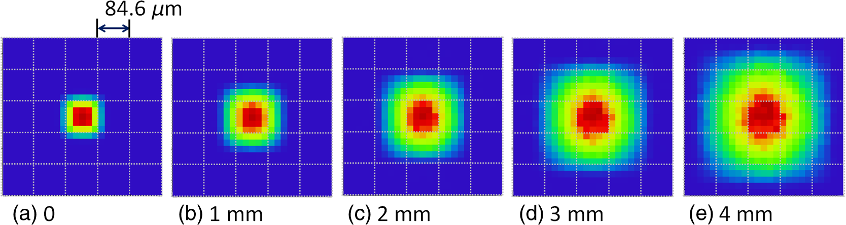 Although the above is designed in geometric optics, in which diffraction may cause stray light, the influence of diffraction is small in this design. As an example, light distribution by diffraction at the second aperture layer is shown in Fig. 6(b), calculated by the following model shown in Fig. 6(a); a point source is placed at object distance of and a slit of is placed at the position of the first aperture layer. The amount of light diffracted to the outside of the geometrical range of is as small as about 7%, and the greatest part is focused near the boundary, meaning that the influence of diffraction is small in this design. However, attention should be paid to diffraction if aiming for resolution higher than 300 dpi with this design. Fig. 6Example of diffraction distribution: (a) model configuration; gap between first and second aperture layers of 0.66 mm is converted thickness in air and (b) diffraction distribution at the second aperture layer calculated in two wavelengths of 0.7 and . The vertical axis is calibrated for the graph area to be 100. 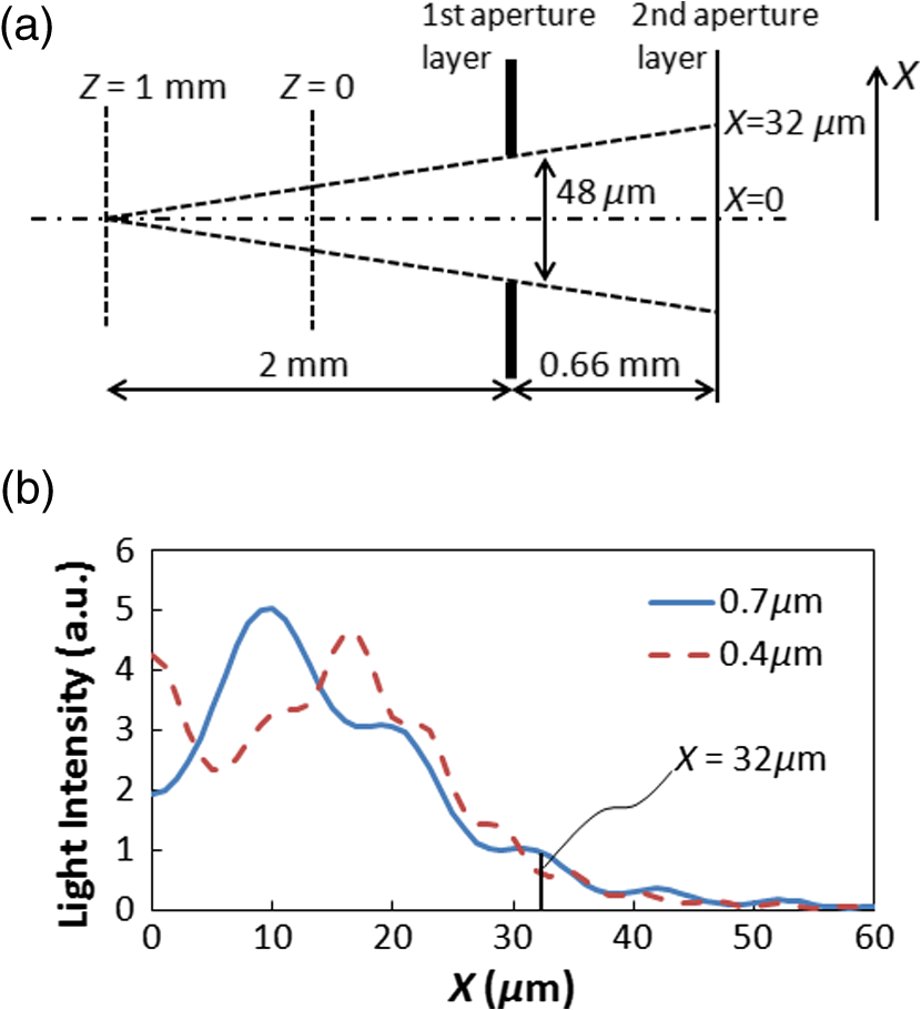 4.ExperimentFigures 7(a) and 7(b) show appearance photos of our prototype sensor, and Figs. 7(c) and 7(d) show the construction. The aperture glass plates with thicknesses of 1.0 and 0.4 mm are deposited on both sides by chromium oxide to make light-shielding layers, before etching the staggered pattern of the aperture arrays. The two glass plates are glued so precisely that each aperture pattern on the two glass plates is matched in position. Then, the set of two aperture glass plates is placed over the image sensor by putting spacers between them. The illumination light guide plate is placed on the aperture glass plate, mixing light from an LED array and illuminating the object with uniform line-shape light. The total thickness is only 5.0 mm, including everything from the illumination light guide plate to the sensor substrate. Additionally, although white LEDs are used and monochrome pictures are taken in this experiment, colorization is easy if three-color LEDs are lighted up in series. Fig. 7Appearance of prototype of lensless image scanner. (a)–(c) Pictures and (d) framework in cross-section. 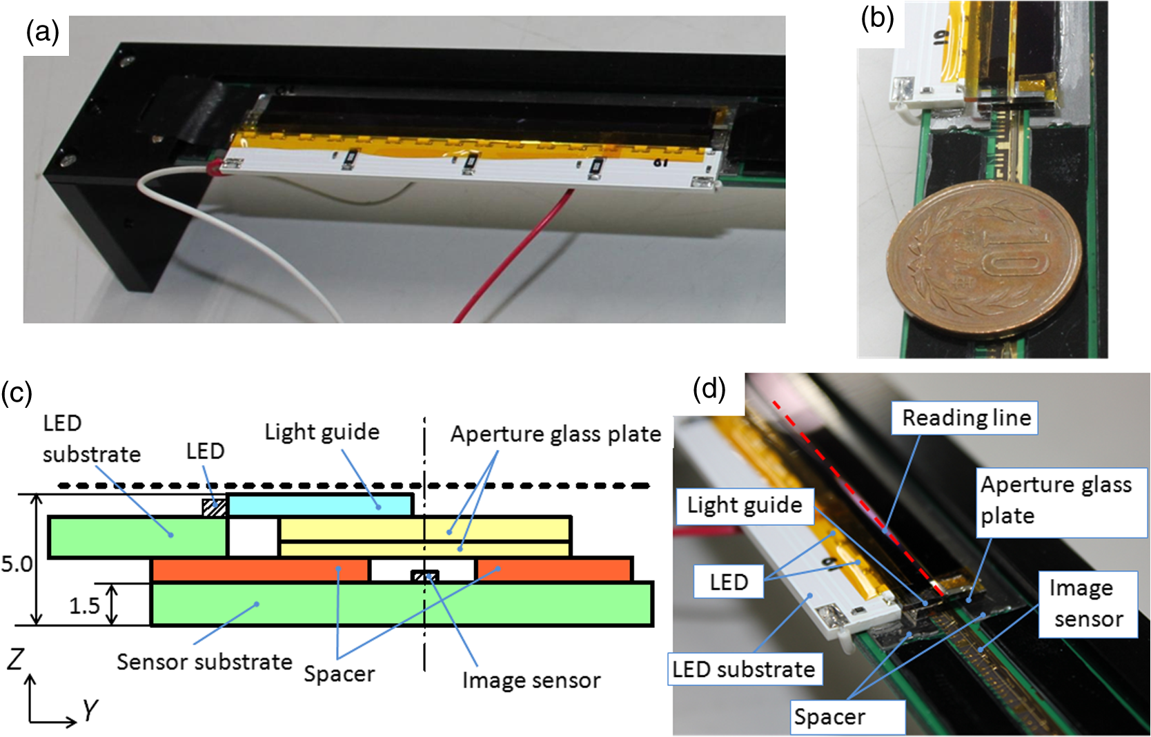 Figures 8 and 9 show sample pictures of 8-pt characters and paper currency at different object distances measured from the top surface of the illumination light guide. The images of 8-pt characters are clearly taken at every object distance in Fig. 8 without any ghost image, though the contrast decreases little by little with the object distance. Paper currency is also pictured clearly. The regular unevenness of the brightness in the direction in Fig. 8(b) is caused by the insufficient uniformity of the illumination. 5.DiscussionThe depth of field is estimated using the reproducibility of contrast by this lensless image scanner. This optics is not an isoplanatic optics, where the point spread function (PSF) does not change over a neighborhood distance. For example, Fig. 10 shows calculated PSFs at the two neighborhood positions: just above an aperture () on the object plane of [Fig. 10(a)] and position shifted by 0.5 pixel in the direction [; Fig. 10(b)]. Since the distributions are substantially different, the normal modulation transfer function (MTF) calculated by Fourier transform of PSF is not suitable. Therefore, ray tracing simulation calculates outputs of the image sensor pixels by placing rectangular charts, which are grating patterns of equally spaced black lines in the direction. Since the Moiré effect appears depending on the period of the rectangular chart, the maximum and minimum values of the waveform are extracted, and the following index is defined as rectangular chart MTF (RMTF) by Eq. (1): Fig. 10PSF on surface of image sensor calculated in ray trace simulation. A point source is placed on the object plane of : (a) just above an aperture () and (b) at shifted position by 0.5 pixel in the direction (). The grid pattern shows image sensor pixels of 600 dpi, and outlined areas in black line show effective pixels. 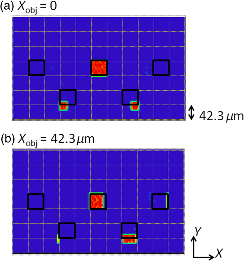 When the period of the rectangular chart is a half-integer multiple of the sensor pixel pitch of , the Moiré effect is suppressed. Therefore, the position of the rectangular chart is shifted bit-by-bit in the direction and the value of Eq. (1) is calculated each time. The maximum value is redefined as RMTF for the period. RMTF is calculated against object distance of in case of pitches of 508, 339, 254, and , which are equivalent to 100, 150, 200, and 247 dpi, respectively. Figure 11 shows the results in solid graphs. Fig. 11RMTF against object distance. Solid lines show simulation results calculated in spatial frequencies of 100, 150, 200, and 247 dpi, equivalent to pitches of 508, 339, 254, and , respectively. Dots show experimental results. 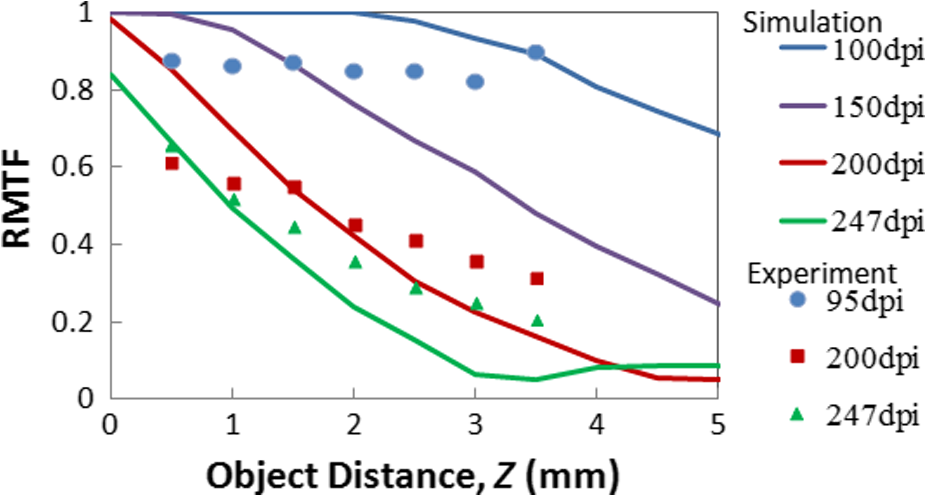 Here, the experimental values of RMTF are shown as dots in Fig. 11. Images of rectangular charts of 95, 200, and 247 dpi are taken by the lensless image scanner, and RMTF values are calculated according to Eq. (1). Figures 12(a) and 12(b) show example images of the 200-dpi test chart at 0.5- and 3.5-mm distances. Figures 12(c) and 12(d) show the intensity profile of the center part of Figs. 12(a) and 12(b), respectively. Comparing the experimental and simulation results, the tendencies are well matched, although the values are not entirely matched. The difference might be caused by misalignment of the assembly of the two aperture glass plates and the image sensor, at least misalignment. Regardless, even when the object distance is as large as 3.5 mm, the RMTF value at 200 dpi is more than 0.3 in the experiment. It can be said that the lensless image scanner has large depth of field of 3.5 mm. Fig. 12Images and profiles of rectangular chart of 200 dpi. (a) 0.5 mm, (b) 3.5 mm, (c) 0.5 mm, and (d) 3.5 mm. 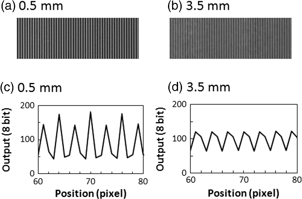 The biggest disadvantage of the lensless image scanner is light efficiency. The light efficiency is estimated by ray trace simulation in comparison with a typical optics shown in Fig. 13, whose magnification ratio is 1. The working -number12 is , which is calculated from two times the focal length divided by the pupil diameter in the case of the same magnification optics. An identical area-light-source emitting diffused rays is placed on the object plane of each model of the lensless image scanner in Fig. 4 and the reference optics in Fig. 13. A detector of 300-dpi pixels is placed on the image plane in Fig. 13, as well. First, the amount of light detected at the lensless image scanner remains unchanged against the object distance. Second, it is 1/36th that of the reference model in Fig. 13. Therefore, the working -number of the lensless image scanner corresponds to in view of light efficiency, derived from multiplying 10 by the square root of 36. The same simulation is performed for a rod-lens-array scanner, producing the result that the light efficiency of the lensless image scanner is about 1/100th that of the rod-lens-array scanner. By the way, this lensless image scanner has much insensitive area because it substitutes a 600-dpi sensor for a 300-dpi sensor, as shown in Fig. 3. If the sensor chip is customized to this lensless image scanner, the sensitive area of 1 pixel can be increased up to four times, resulting in four times greater light efficiency. Though the light efficiency is still 1/25th that of the rod-lens-array scanner, scanning speed for a mobile scanner is not required to be as fast as for copiers in an office. Therefore, the disadvantage in light efficiency would not be fatal. Fig. 13Reference model for estimation of light efficiency. The focal length of the lens is 10 mm and the aperture size is 2 mm. A flat surface light source and a detector are placed 20 mm away from the lens. Working -number is . 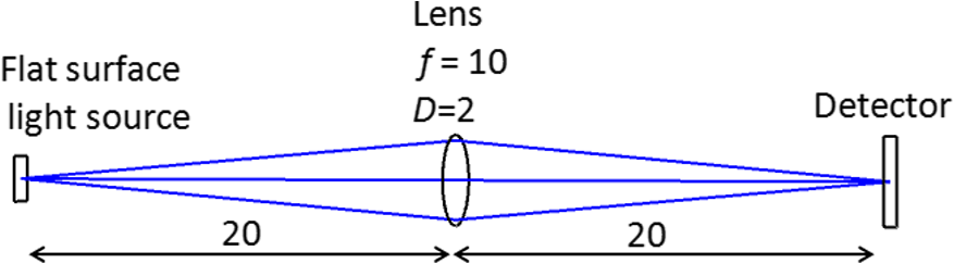 Figure 14 shows a concept model for a future lensless image scanner. Since the sensor substrate is made of glass and the backilluminated sensor is mounted with the sensitive surface facing the substrate, the total thickness could be thinner; the sensor substrate thickness of 1.5 mm could be reduced from the total thickness of 5 mm in Fig. 7. The lensless image scanner has an advantage in thickness compared, for example, to a rod-lens-array scanner, whose thickness is at least 15 mm. 6.SummaryWe proposed a lensless image scanner with a large depth of field by a new structure, acting like an optical stamp. Aperture arrays, whose patterns are staggered in two lines, are layered in three on two glass plates glued to each other, and they make a one-to-one correspondence between image sensor pixels and scattering points on the object plane by shielding stray light passing obliquely. We manufactured the prototype model of 300-dpi resolution, whose height is as little as 5 mm. The pictures taken by the prototype model showed that ghost images are well restricted if the assembly is arranged with high accuracy. Also, the images of test charts showed that our sensor has a large depth of field of 3.5 mm, defined as a range of over 30% of RMTF in a spatial frequency corresponding to 200 dpi. ReferencesR. H. Dicke,
“Scatter-hole cameras for x-rays and gamma rays,”
J. Astrophys., 153 L101
–L106
(1968). http://dx.doi.org/10.1086/180230 JASRD7 0250-6335 Google Scholar
J. G. Ables,
“Fourier transform photography: a new method for x-ray astronomy,”
Proc. Astron. Soc. Aust., 1
(4), 172
–173
(1968). Google Scholar
E. E. Fenimore and T. M. Canon,
“Coded aperture imaging with uniformly redundant arrays,”
Appl. Opt., 17
(3), 337
–347
(1978). http://dx.doi.org/10.1364/AO.17.000337 APOPAI 0003-6935 Google Scholar
M. J. DeWeert and B. P. Farm,
“Lensless coded-aperture imaging with separable Doubly-Toeplitz masks,”
Opt. Eng., 54
(2), 023102
(2015). http://dx.doi.org/10.1117/1.OE.54.2.023102 Google Scholar
G. Huang et al.,
“Lensless imaging by compressive sensing,”
in IEEE Int. Conf. Image Processing,
2101
–2105
(2013). http://dx.doi.org/10.1109/ICIP.2013.6738433 Google Scholar
D. G. Stork and P. R. Gill,
“Lensless ultra-miniature CMOS computational imagers and sensors,”
in Int. Conf. on Sensor Technologies and Applications,
186
–190
(2013). Google Scholar
H. Kakinuma et al.,
“Direct-contact type image sensors using a novel amorphous-silicon photodiode array,”
IEEE Electron Device Lett., 12
(8), 413
–415
(1991). http://dx.doi.org/10.1109/55.119149 Google Scholar
M. Kawazu and Y. Ogura,
“Application of gradient-index fiber arrays to copying machines,”
Appl. Opt., 19
(7), 1105
–1112
(1980). http://dx.doi.org/10.1364/AO.19.001105 APOPAI 0003-6935 Google Scholar
K. Uchida,
“Fingerprint identification,”
NEC J. Adv. Technol., 2
(1), 19
–27
(2005). Google Scholar
H. Kawano et al.,
“Compact image scanner with large depth of field by compound eye system,”
Opt. Express, 20
(12), 13532
–13538
(2012). http://dx.doi.org/10.1364/OE.20.013532 OPEXFF 1094-4087 Google Scholar
H. Kawano et al.,
“Practical design for compact image scanner with large depth of field by compound eye system,”
Opt. Express, 22
(15), 18010
–18019
(2014). http://dx.doi.org/10.1364/OE.22.018010 OPEXFF 1094-4087 Google Scholar
J. E. Greivenkamp, Field Guide to Geometrical Optics, SPIE Press, Bellingham, Washington
(2004). Google Scholar
BiographyHiroyuki Kawano is an optical engineer at Mitsubishi Electric Corp. in Japan. He received his BS and MS degrees in physics from the University of Tokyo in 1994 and 1996, respectively, and his PhD degree in engineering from the University of Kyoto in 2011. His current research interests include optical design and imaging systems. He is a member of SPIE. |