|
|
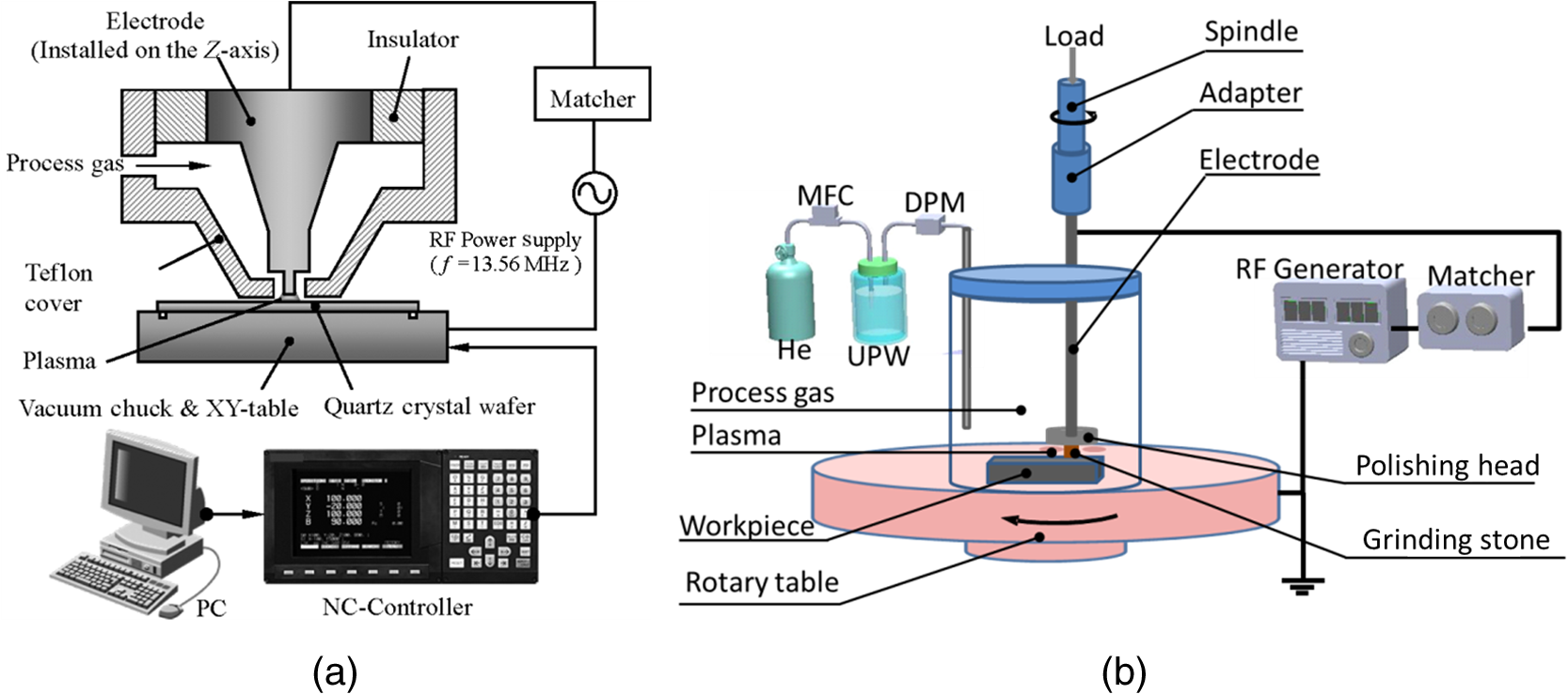
1.IntroductionReaction-sintered silicon carbide (RS-SiC) ceramic is a promising optical material because of its excellent mechanical, chemical, thermal, and electrical properties,1,2 which makes it a research focus in the field of optical machining. However, it is difficult to obtain a high material removal rate (MRR) in figuring RS-SiC for its high mechanical hardness and strong chemical inertness.3,4 What is more, the fabrication process of RS-SiC generates SiC and Si domains in the RS-SiC substrate, and the asymmetric components make it difficult to obtain a high surface quality in the fine finishing of RS-SiC.5,6 Along with the increasing demands of RS-SiC products with high quality, it is urgently required to develop unique processing techniques. Many techniques have been developed to process this traditional difficult-to-machine material, but few of them can simultaneously obtain high MRR and fine surface quality in machining RS-SiC.7 An efficient way is the combination of a rapid figuring method and a fine finishing method. Plasma chemical vaporization machining (PCVM) is a machining method with chemical material removal by the F radical.8,9 Owing to the controllable chemical reaction rate, the MRR in PCVM can be enlarged by adjusting the processing parameters.10 Plasma-assisted polishing (PAP) includes the oxidation of the substrate by the water vapor plasma and the removal of oxide by the abrasive polishing.11 Due to the hardness differences between the substrate and oxide, PAP can achieve an ultrasmooth surface, which has been verified in machining single crystal 4H-SiC samples.12,13 Therefore, the application of atmospheric-pressure plasma-based chemical dry figuring and finishing, which consist of PCVM and PAP, is investigated to verify its feasibility to process RS-SiC in this study. After PCVM of RS-SiC samples, scanning white-light interferometer (SWLI) measurement was conducted to calculate the MRR and evaluate the surface quality, and the scanning electron microscope (SEM) and the atomic force microscope (AFM) were used to investigate the surface morphology. Meanwhile, PAP was applied to improve the surface quality of the processed RS-SiC sample in PCVM, and the surface roughnesses corresponding to different polishing parameters were obtained by SWLI measurements. By the investigation on MRR in PCVM and the study on surface quality in PAP, the feasibility of these techniques was verified. 2.Experimental ApparatusThe schematic diagram of the PCVM system is shown in Fig. 1(a).14,15 The electrode for generating plasma was constructed from coaxially arranged metal electrode and alumina () ceramic tube. The diameter and material of the electrode were 3 mm and aluminum (Al) alloy, respectively. The composition and flow rate of the processing gas were controlled by the mass flow controller. Supplying of the gas from the circumference of the tip of the electrode replaced the air to the processing gas and enabled the stable generation of the plasma in the atmospheric-pressure environment. The applied high-frequency electric field () generated the plasma in the narrow gap between the electrode and the substrate, and the typical gap distance was . The schematic diagram of the PAP system is shown in Fig. 1(b).16,17 The compound apparatus consisted of the installed plasma generation part and the mechanical polishing part. Atmospheric-pressure plasma was generated by applying an RF () electric power, and helium (He)-based water vapor with a flow rate of was supplied as the process gas. Water vapor was introduced into the process gas by bubbling the He through ultrapure water, and its concentration was measured by the dew-point meter. The used copper (Cu) electrode was covered with quartz glass to prevent the arc discharge in the generation of dielectric barrier discharge. In the mechanical polishing part, the RS-SiC sample was fixed on the rotary table. The resin bonded ceria () grinding stone was installed on the polishing head. An insulative adapter was used to connect the spindle and the electrode, which could protect the motor. The load was set to 10 g, which was propitious to obtain high surface quality in the polishing process. First, the RS-SiC sample was processed by PCVM. Afterward, PAP was conducted to finish the surface of the processed RS-SiC sample in PCVM. 3.Results and Discussion3.1.Reaction-Sintered Silicon Carbide Sample Processed by Plasma Chemical Vaporization MachiningThe MRR of RS-SiC in PCVM was obtained by SWLI measurement, as shown in Fig. 2. The RF power, compositions and flow rates of the process gases, and machining time were 100 W, He (), (), (), and 90 s, respectively. It could be calculated that the peak-MRR was , and the volume-MRR was . Relative to the present methods for machining RS-SiC, such as the single-point diamond turning,18 electrolytic in-process dressing grinding,19 and magnetorheological finishing,20 the MRR in PCVM of RS-SiC is considerable. What is more, PCVM is a noncontact figuring technique and the material removal is conducted by chemical reaction, so we suppose that there will be no subsurface damage or residual stresses on the processed sample, which are common in the processed RS-SiC sample obtained by the present mechanical material removal methods. Therefore, PCVM can be treated as an efficient rapid figuring method to process RS-SiC. Fig. 2Calculation of the MRR in PCVM of RS-SiC sample obtained by SWLI measurement: (a) typical shape of the removal spot and (b) cross-sectional line of the removal spot. 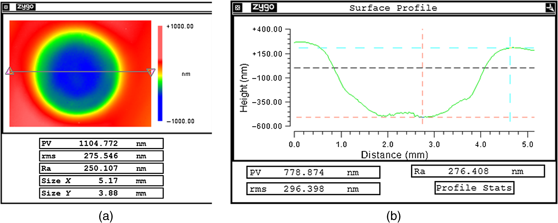 The comparisons of surface roughness of the RS-SiC sample before and after PCVM are shown in Fig. 3. It can be found that the initial surface, which was obtained by diamond lapping, had a fine surface roughness rms 0.910 nm. However, from Fig. 3(a), it can be found that there were scratches on the surface, because the hardness of the diamond is higher than that of the RS-SiC. Furthermore, there were small holes on the surface as shown in Fig. 3(a), because the hardnesses of SiC and Si grains in the RS-SiC substrate differ, which resulted in a different micro-MRR among the different grains. After PCVM, the RS-SiC surface was deteriorated, and the surface roughness root-mean-square (rms) and roughness average (Ra) were 382.116 and 242.427 nm, respectively. The major reason for this phenomenon might be that the chemical reactivities of SiC and Si grains differ. The possible chemical reactions that occurred in the PCVM of RS-SiC are as follows: Therefore, the MRRs in machining SiC/Si grains by F radicals were nonuniform. The results obtained by SWLI indicated that the PCVM could obtain high MRR in processing RS-SiC but the obtained surface quality was rough. Thus, another method is urgently demanded to improve the surface quality of the processed RS-SiC in PCVM, which can form an integrated technique.Fig. 3Comparisons of surface roughness of the RS-SiC sample before and after PCVM: (a) the initial surface obtained by diamond lapping and (b) the processed surface obtained by PCVM. 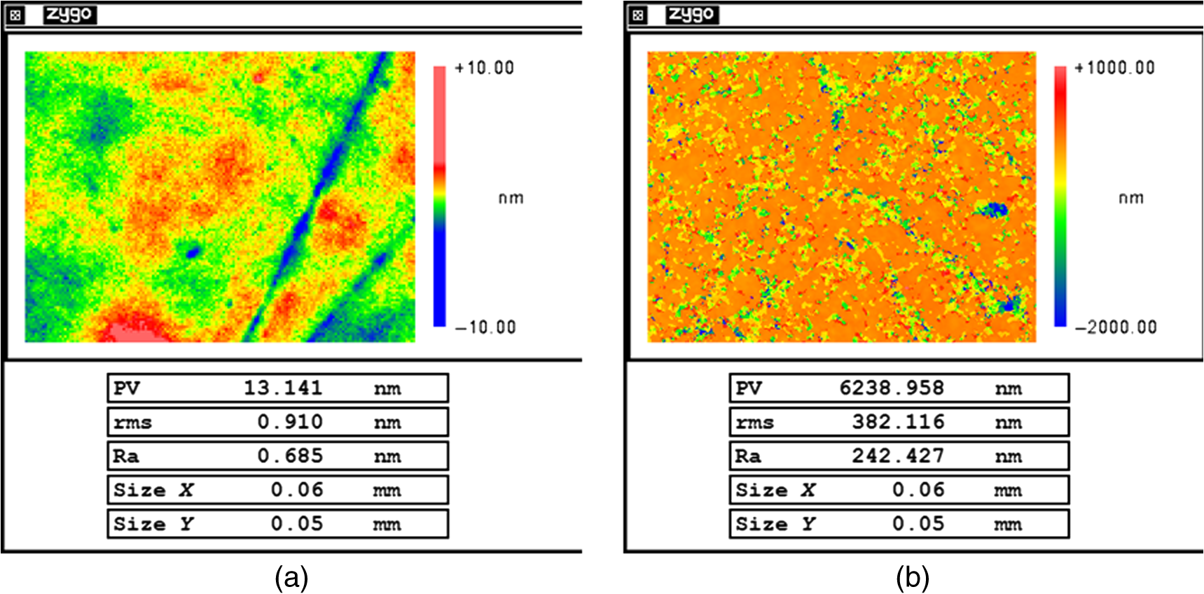 The comparisons of the surface morphology of RS-SiC before and after PCVM at the same position were conducted by SEM, as shown in Fig. 4. From Fig. 4(a), it could be found that there were many small scratches and holes on the initial surface generated by diamond lapping, which was in accordance with the characters exhibited in Fig. 3(a). The surface of the processed RS-SiC sample in PCVM was bumpy, as shown in Fig. 4(b). Irregular holes were formed at the region of initial Si grains, and the areas of initial SiC grains had relatively smooth surfaces. It could be concluded that the micro-MRR of Si grain was larger than that of SiC grain in the RS-SiC substrate. This phenomenon coincided with the fact that the MRR in PCVM of single crystal Si wafer is larger than that of single crystal SiC wafer under the same experimental parameters.21 Fig. 4Comparisons of the surface morphology of RS-SiC sample at the same position obtained by SEM: (a) before and (b) after PCVM. 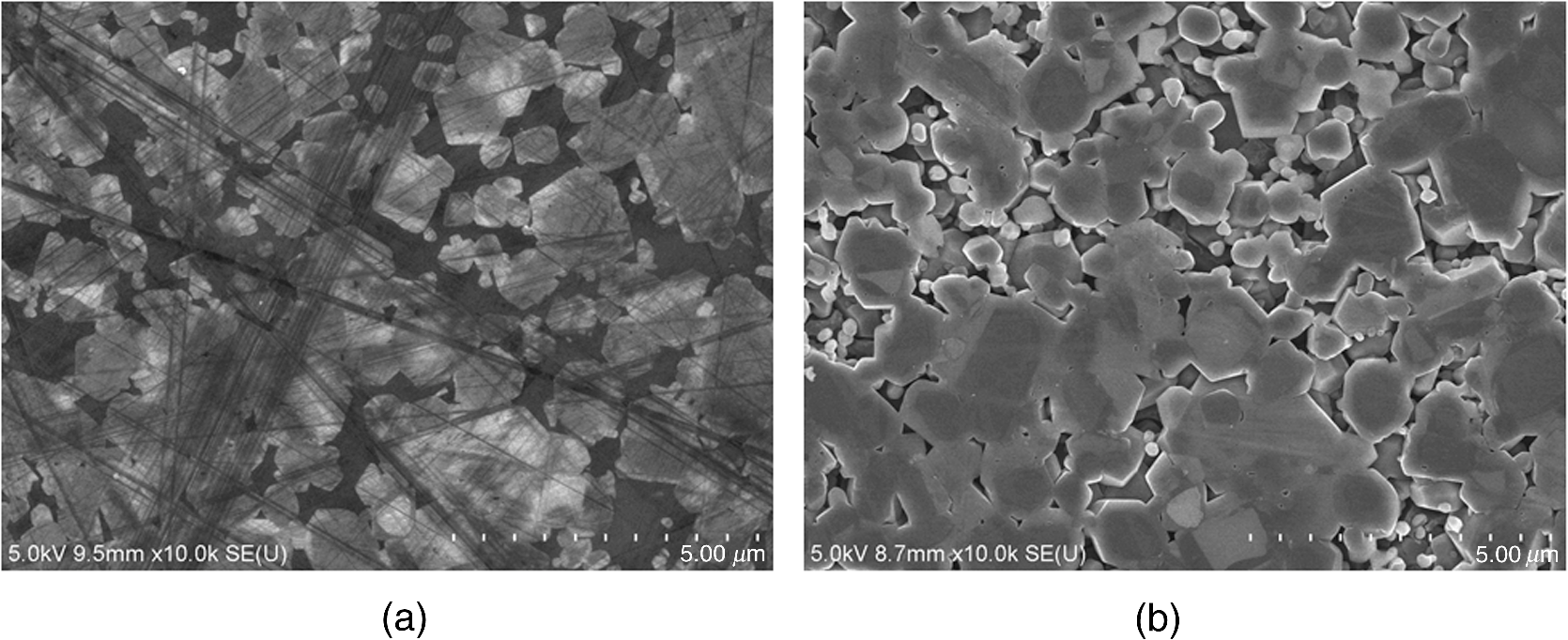 The details of the processed RS-SiC sample in PCVM are shown in Fig. 5, which were obtained by SEM observation under high magnification. The outlines of the newly exposed SiC grains were very clear in Fig. 5(a), especially for some large grains. Meanwhile, there were obvious boundaries among the newly revealed Si grain and the SiC grains around it, as shown in Fig. 5(b), and the Si grain had the same characters as the amorphous silicon. What is more, sizes of the SiC grains were shrunken, as shown in Fig. 5(c), because the material removal in PCVM was conducted from the external to the internal on a SiC grain. Furthermore, the connects among different SiC grains were weakened, and there were some almost dissociative SiC grains, as shown in Figs. 5(c) and 5(d), because the chemical reaction rate in the boundary region was larger than that in the central area. Finally, these bumpy structures on the processed RS-SiC could decrease the surface hardness, and the contacting areas between the polishing particle and the abraded sample could be increased. All these features were propitious to improve the surface quality and the MRR in the further PAP process. Fig. 5Details of the processed RS-SiC sample in PCVM obtained by SEM observation under high magnification: (a) the newly exposed SiC grains, (b) the newly revealed Si grains, (c) the shrunken SiC grains, and (d) the weakened connects among different SiC grains. 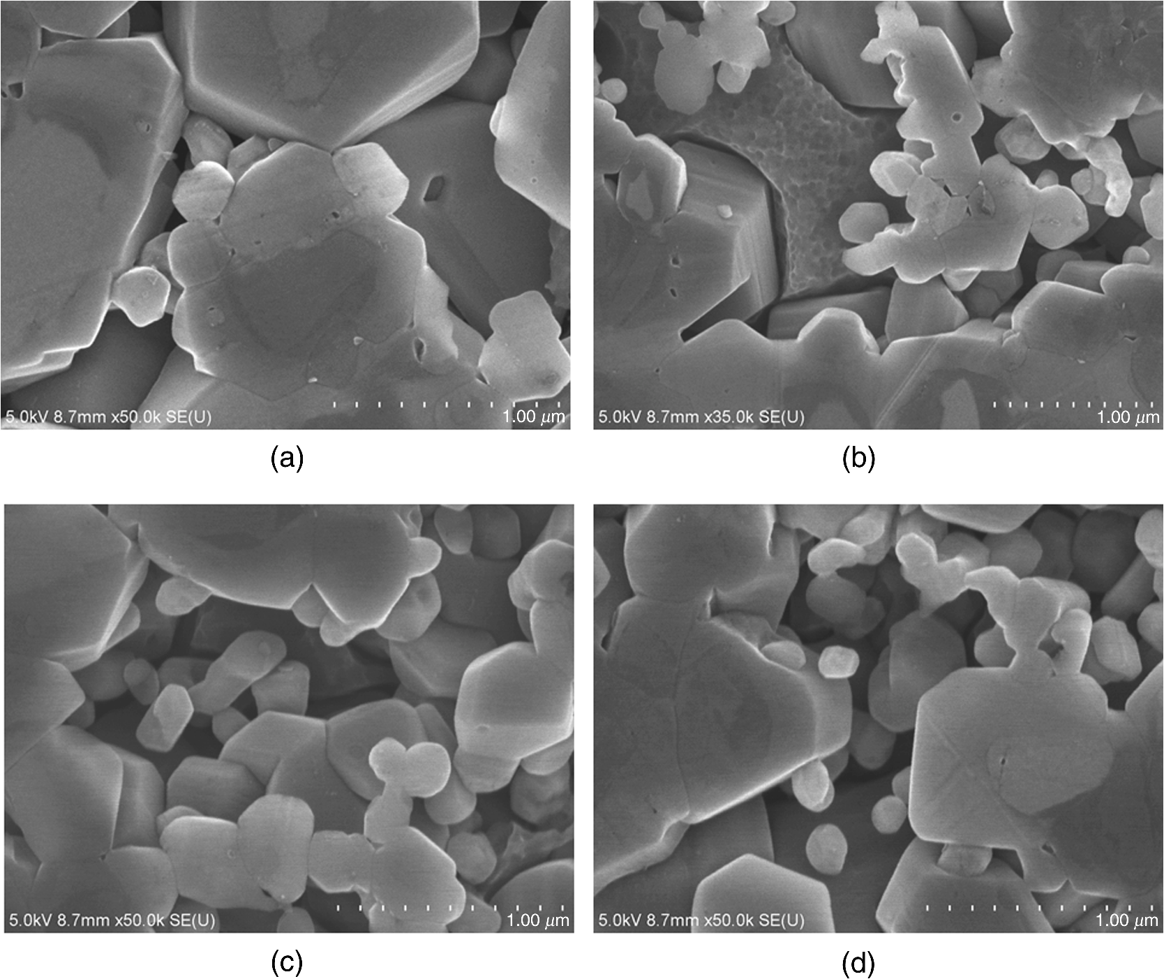 Quantitative analysis of surface morphology of the processed RS-SiC sample in PCVM was obtained by AFM, as shown in Fig. 6. Surfaces of the processed SiC grains in RS-SiC substrate almost remained in a plane, which could be judged from the profile of the cross-sectional line shown in Fig. 6(b). What is more, there were many holes formed at the initial Si regions, and depths of the holes varied from 20 to 60 nm, which further validated the characteristics in PCVM of RS-SiC sample. Fig. 6Quantitative analysis of surface morphology of the processed RS-SiC sample in PCVM by AFM: (a) surface morphology and (b) profile of the cross-sectional line.  From research on the MRR, surface quality, and surface morphology of the processed RS-SiC sample in PCVM, it could be concluded that PCVM could be treated as an efficient method for the rapid figuring of RS-SiC, and the surface quality should be further improved. 3.2.Reaction-Sintered Silicon Carbide Sample Processed by Plasma-Assisted PolishingThe PCVM processed RS-SiC sample was further processed by PAP to improve the surface quality. The investigated RS-SiC sample was shown in Fig. 7. The process parameters in PCVM were summarized in Table 1. The size of the RS-SiC sample was . The size of the processed area in PCVM was , which was realized by controlling the apparatus in Fig. 1(a) in the raster scanning mode with the scan speed of and feed pitch of 1 mm. Table 1Experimental parameters in processing RS-SiC by PCVM.
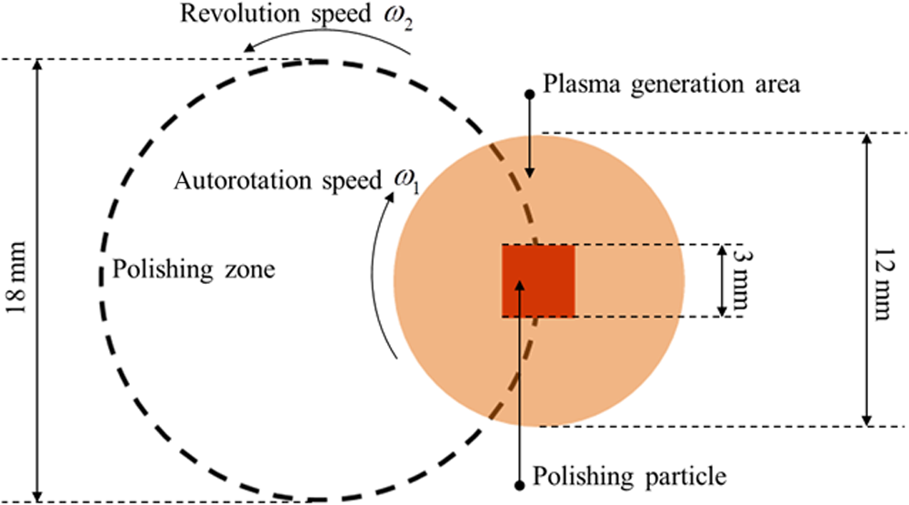
The parameters in processing RS-SiC by the PAP were summarized in Table 2. The schematic diagram of the PAP process was shown in Fig. 8. The autorotation speed and revolution speed were adjusted to compare the machining results when other parameters were confirmed. Table 2The summarized experimental parameters in processing RS-SiC by PAP.
The generation rate of the oxide layer was established when the RF power, process gases, and their flow rates were confirmed. The MRR of the oxide layer could be controlled by adjusting the autorotation speed and revolution speed when the type of grinding stone (polishing particle) and its size, polishing head and its size, and eccentricity were assigned. In the experimental apparatus of PAP as shown in Fig. 1(b), there were five levels for both the autorotation motor and the revolution motor. The selected experiments were organized in 11 groups corresponding to the different collocations of autorotation speed and revolution speed, as shown in Table 3, which aimed to seek the optimal processing parameters. Table 3The summarized collocations of autorotation speed and revolution speed in PAP.
After PAP, the processed RS-SiC samples were observed by SWLI to evaluate the surface roughness, and the results were shown in Fig. 9. For the purpose of conveniently comparing the surface quality, the obtained surface roughness rms in Fig. 9 was summarized in Table 4. It could be found that the optimal collocation was group 2 (corresponding to and ), in which the obtained surface roughness rms was 2.186 nm, as shown in Fig. 9(b). Meanwhile, the worst result appeared in the group 11 (corresponding to and ), in which the achieved surface roughness rms was 13.080 nm, as shown in Fig. 9(k). The experimental results indicated that surface quality of the processed RS-SiC in PAP was obviously better than that of the surface obtained by PCVM [Fig. 3(b)] and slightly worse than that of the surface obtained by diamond lapping [Fig. 3(a)]. Meanwhile, there were no visible subsurface damages or scratches on the processed sample in PAP, because the hardness of the ceria abrasive grain was smaller than that of the RS-SiC substrate and almost equal to that of the oxide layer. Relative to the obtained ultrasmooth surface (roughness rms 0.629 nm) in the divided PAP (D-PAP) process,5 the achieved surface quality in the simultaneous PAP (S-PAP) could be improved by optimizing the process parameters. Meanwhile, the rate in plasma oxidation of RS-SiC was low and the oxide layer prevented the former oxidation of subsurface layer. What is more, in D-PAP, the oxidation and the polishing processes were divided, which indicated that the MRR in D-PAP was obviously smaller than that in S-PAP. Therefore, S-PAP was more suitable for the fine finishing of the RS-SiC sample. Fig. 9Evaluations of surface qualities of the processed RS-SiC in PAP corresponding to the different groups: (a) and , (b) and , (c) and , (d) and , (e) and , (f) and , (g) and , (h) and , (i) and , (j) and , (k) and , and (l) the summarized data. 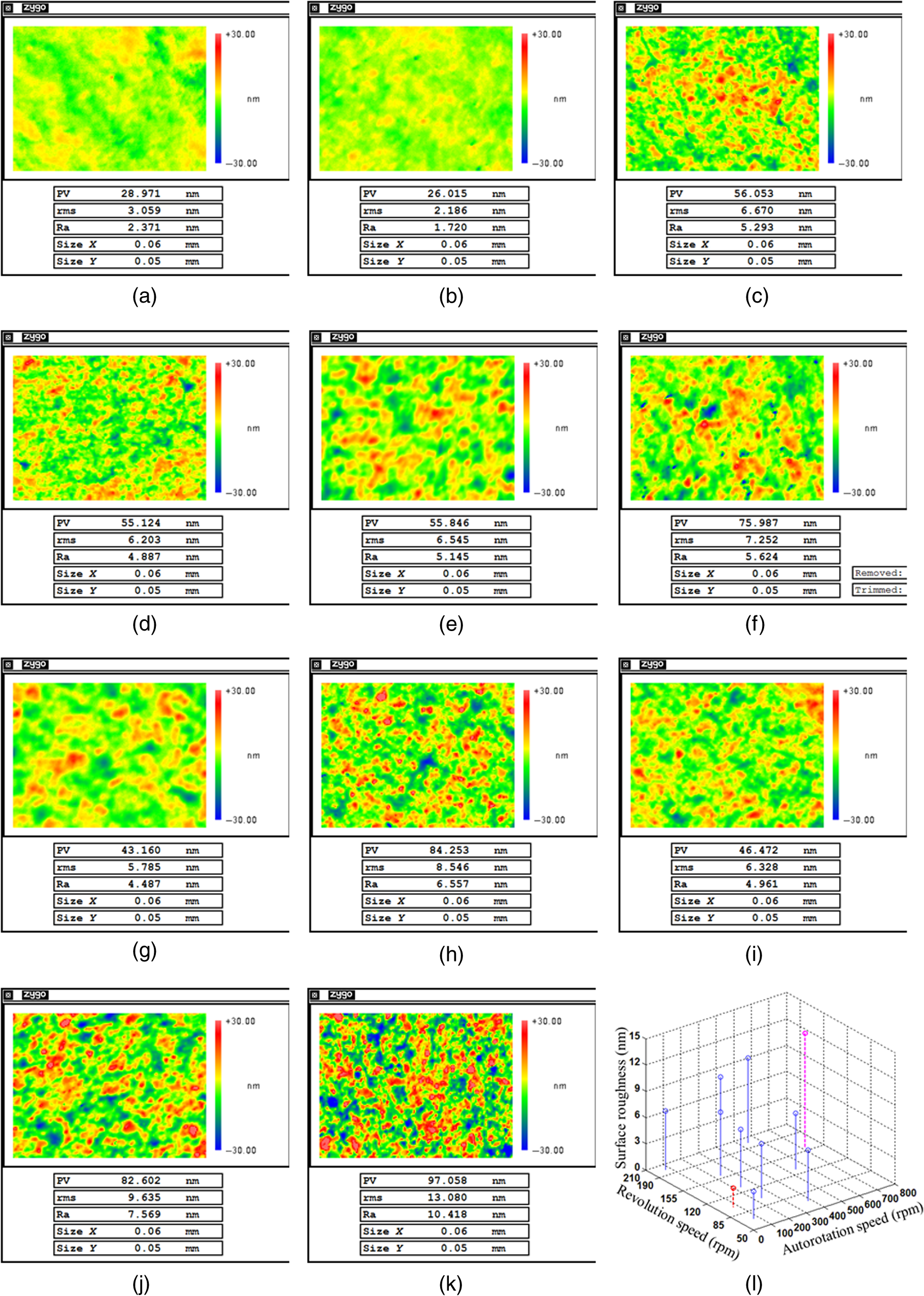 Table 4The obtained surface roughness rms of the polished RS-SiC sample in each group.
The surface quality of the processed RS-SiC sample in PAP was determined by matching the MRR of oxide layer with its generation rate . In this study, the plasma oxidation rate of the RS-SiC sample was confirmed by the experimental parameters listed in Table 2, and the MRR of the oxide layer could be controlled by adjusting the autorotation speed and the revolution speed . Although the actual values of and are difficult to obtain, they could be confirmed under certain experimental conditions. If , the generation of oxide layer entirely matched its removal, which could obtain a relatively smooth surface roughness, as shown in Fig. 9(b), and the PAP of RS-SiC could simultaneously obtain a high MRR and smooth surface in this condition. When , the oxide layer could not be removed completely and the polishing process was equal to the polished silica () component by ceria abrasion, which was difficult to obtain an ultrasmooth surface, as shown in Fig. 9(a). Otherwise if , after removal of the oxide layer, the ceria abrasive continued to polish the RS-SiC substrate. The ceria abrasive was seriously abraded, because the hardness of the ceria abrasive grain was distinctly smaller than that of the RS-SiC. The wear degree of the ceria abrasive grain was aggravated along with the increasing of and , which resulted in a worse surface quality of the processed RS-SiC sample in PAP, as shown in Figs. 9(c)–9(k). The experimental results indicated that parameters in PAP of RS-SiC should be strictly selected, and the optimal parameters simultaneously could obtain high MRR and smooth surface. 4.ConclusionsThe combination of PCVM and PAP was conducted to verify the feasibility of these techniques for processing an RS-SiC substrate, which was aimed to improve the MRR in rapid figuring and ameliorate the surface quality in fine finishing. The following conclusions were obtained in this study:
The combination of PCVM and PAP can be treated as a technique for RS-SiC, which can improve the machining level of RS-SiC samples and promote the application of RS-SiC products. AcknowledgmentsThis work was supported by a grant from the National Key Research and Development Program (Grant No. 2016YFC0802903), a grant from the National Natural Science Foundation of China (Grant No. 51505498), and a grant from the Natural Science Foundation of Jiangsu Province (Grant No. BK20150714). The authors also express their gratitude to the staffs and students of the Research Center for Ultra-Precision Science and Technology, Osaka University. ReferencesZ. R. Huang et al.,
“Manufacture of large-scale lightweight SiC mirror for space,”
Proc. SPIE, 8335 83351R
(2012). http://dx.doi.org/10.1117/12.917585 PSISDG 0277-786X Google Scholar
J. S. Johnson, K. Grobsky and D. J. Bray,
“Rapid fabrication of lightweight silicon carbide mirrors,”
Proc. SPIE, 4771 243
–253
(2002). http://dx.doi.org/10.1117/12.482166 PSISDG 0277-786X Google Scholar
S. P. Lee et al.,
“Fabrication of liquid phase sintered SiC materials and their characterization,”
Fusion Eng. Des., 81
(8–14), 963
–967
(2006). http://dx.doi.org/10.1016/j.fusengdes.2005.09.025 FEDEEE 0920-3796 Google Scholar
S. Suyama, T. Kameda and Y. Itoh,
“Development of high-strength reaction-sintered silicon carbide,”
Diamond Relat. Mater., 12
(3–7), 1201
–1204
(2003). http://dx.doi.org/10.1016/S0925-9635(03)00066-9 DRMTE3 0925-9635 Google Scholar
X. M. Shen et al.,
“Mechanism analysis on finishing of reaction-sintered silicon carbide by combination of water vapor plasma oxidation and ceria slurry polishing,”
Opt. Eng., 54
(5), 055106
(2015). http://dx.doi.org/10.1117/1.OE.54.5.055106 OPEGAR 0091-3286 Google Scholar
Q. Z. Tu et al.,
“Efficient processing of reaction-sintered silicon carbide by anodically oxidation-assisted polishing,”
Opt. Eng., 54
(10), 105113
(2015). http://dx.doi.org/10.1117/1.OE.54.10.105113 Google Scholar
J. W. Yan, Z. Y. Zhang and T. Kuriyagawa,
“Mechanism for material removal in diamond turning of reaction-bonded silicon carbide,”
Int. J. Mach. Tools Manuf., 49
(5), 366
–374
(2009). http://dx.doi.org/10.1016/j.ijmachtools.2008.12.007 Google Scholar
K. Yamamura, S. Shimada and Y. Mori,
“Damage-free improvement of thickness uniformity of quartz crystal wafer by plasma chemical vaporization machining,”
CIRP Ann.–Manuf. Technol., 57
(1), 567
–570
(2008). http://dx.doi.org/10.1016/j.cirp.2008.03.132 Google Scholar
Y. Takeda et al.,
“Open-air type plasma chemical vaporization machining by applying pulse-width modulation control,”
J. Phys. D Appl. Phys., 47
(11), 115503
(2014). http://dx.doi.org/10.1088/0022-3727/47/11/115503 JPAPBE 0022-3727 Google Scholar
H. Takino et al.,
“Shape correction of optical surfaces using plasma chemical vaporization machining with a hemispherical tip electrode,”
Appl. Opt., 51
(3), 401
–407
(2012). http://dx.doi.org/10.1364/AO.51.000401 APOPAI 0003-6935 Google Scholar
K. Yamamura et al.,
“Plasma assisted polishing of single crystal SiC for obtaining atomically flat strain-free surface,”
CIRP Ann. Manuf. Technol., 60 571
–574
(2011). http://dx.doi.org/10.1016/j.cirp.2011.03.072 Google Scholar
H. Deng et al.,
“Damage-free dry polishing of 4H-SiC combined with atmospheric-pressure water vapor plasma oxidation,”
Jpn. J. Appl. Phys., 50
(8), 08JG05
(2011). http://dx.doi.org/10.7567/JJAP.50.08JG05 JJAPA5 0021-4922 Google Scholar
K. Yamamura et al.,
“High-integrity finishing of 4H-SiC (0001) by plasma-assisted polishing,”
Adv. Mater. Res., 126–128 423
–428
(2010). http://dx.doi.org/10.4028/www.scientific.net/AMR.126-128 Google Scholar
Y. Mori, K. Yamamura and Y. Sano,
“Thinning of silicon-on-insulator wafers by numerically controlled plasma chemical vaporization machining,”
Rev. Sci. Instrum., 75
(4), 942
–946
(2004). http://dx.doi.org/10.1063/1.1687041 RSINAK 0034-6748 Google Scholar
Y. Mori, K. Yamamura and Y. Sano,
“The study of fabrication of the x-ray mirror by numerically controlled plasma chemical vaporization machining: development of the machine for the x-ray mirror fabrication,”
Rev. Sci. Instrum., 71
(12), 4620
–4626
(2000). http://dx.doi.org/10.1063/1.1322580 RSINAK 0034-6748 Google Scholar
H. Deng, M. Ueda and K. Yamamura,
“Chemical and morphological analysis of 4H-SiC surface processed by plasma assisted polishing,”
Key Eng. Mater., 516 186
–191
(2012). http://dx.doi.org/10.4028/www.scientific.net/KEM.516 KEMAEY 1013-9826 Google Scholar
H. Deng and K. Yamamura,
“XTEM observation of 4H-SiC (0001) surfaces processed by plasma assisted polishing,”
Adv. Mater. Res., 497 156
–159
(2012). http://dx.doi.org/10.4028/>www.scientific.net/AMR.497 Google Scholar
H. Y. Tam, H. B. Cheng and Y. W. Wang,
“Removal rate and surface roughness in the lapping and polishing of RB-SiC optical components,”
J. Mater. Process. Technol., 192–193 276
–280
(2007). http://dx.doi.org/10.1016/j.jmatprotec.2007.04.091 JMPTEF 0924-0136 Google Scholar
H. Katahira and H. Ohmori,
“ELID grinding characteristics and surface analysis for micro fabrication of advanced ceramics,”
Key Eng. Mater., 339 483
–489
(2007). http://dx.doi.org/10.4028/www.scientific.net/KEM.339 KEMAEY 1013-9826 Google Scholar
H. Zhu et al.,
“Rapid fabrication of lightweight SiC mirror using CCOS,”
Proc. SPIE, 8194 81942A
(2011). http://dx.doi.org/10.1117/12.900575 PSISDG 0277-786X Google Scholar
K. Yamamura, Y. Yamamoto and H. Deng,
“Preliminary study on chemical figuring and finishing of sintered sic substrate using atmospheric pressure plasma,”
Procedia CIRP, 3 335
–339
(2012). http://dx.doi.org/10.1016/j.procir.2012.07.058 Google Scholar
BiographyXinmin Shen received his BS, MS, and PhD degrees in mechanical engineering from the National University of Defense Technology in 2008, 2010, and 2014, respectively. He is a lecturer at the PLA University of Science and Technology. From 2011 to 2013, he studied in Osaka University as a special research student. He is the author of more than 20 papers. His current research focuses on the ultraprecision machining of optical components. Kazuya Yamamura received his PhD in engineering from Osaka University in 2001. He is an associate professor at Osaka University. His research area is development of unconventional ultraprecision manufacturing process and its application, such as figuring, finishing, functionalization, utilizing reactive plasma, or electrochemical process. |
||||||||||||||||||||||||||||||||||||||||||||||||||||||||||||||||||||||||||||||||||||||||||||||||||||||||||||||