|
|
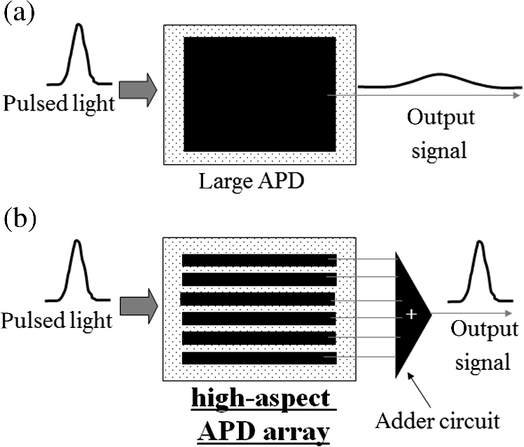
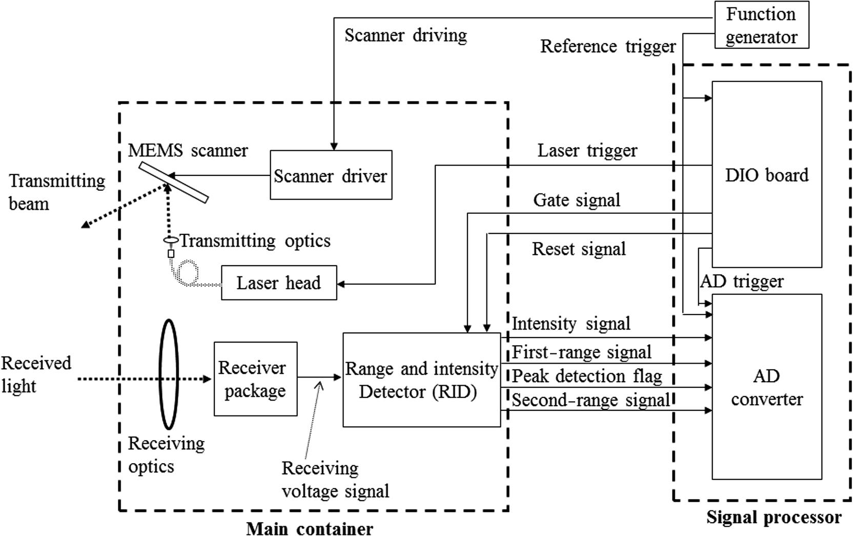
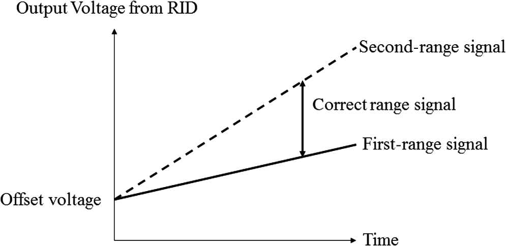
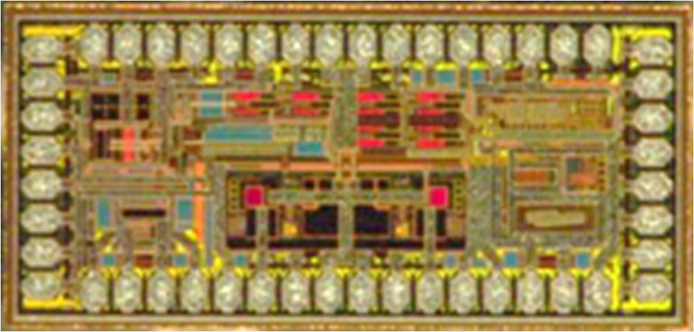
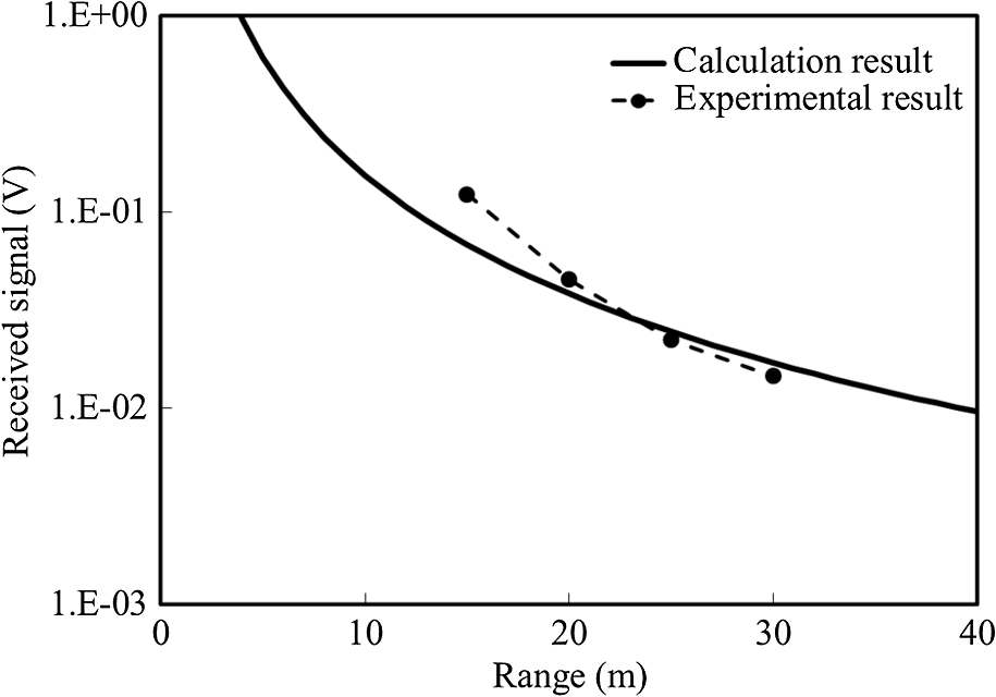
1.IntroductionThe range imaging laser sensor,1,2 which utilizes the time of flight (TOF) of a laser light, is a real-time remote sensor that offers three-dimensional information of scenes. This sensor has the potential for many applications, including robotics, terrain visualization, augmented vision, and reconnaissance. Various types of this sensor have been developed. Stettner et al.,3 Dries et al.,4 Vaidyanathan et al.,5 Yuan et al.,6 and Borniol et al.7 proposed the “flash” type laser sensor, which has a scanless two-dimensional (2-D) array receiver. This sensor acquires the range image with one transmitted beam, which illuminates the whole field of view (FOV) area of the array receiver. This type is suitable for the extremely high frame rate imaging, because of its capability of instantaneous imaging for all pixels. However, this sensor is difficult to realize long-range imaging, since the transmitted beam is divided into many parts corresponding to the elements of the array receiver. Accordingly, a received power of a backscattered light for each element decreases distinctly because of the above-mentioned division. Furthermore, this sensor configuration is complicated, since it needs a complex control circuit for the parallel operation of the array receiver having many elements. Garcia et al.8 and Inoue et al.9 proposed the “coaxial optics and scanning” type, which has a scanner for both the transmitted beam and FOV with a single-element receiver. This sensor is easy to achieve long-range imaging with its simple system configuration, since the problem of the above-mentioned power division in the case of the flash type does not exist for this single-element receiver type. However, the sensor is not suitable for the high frame rate imaging, since the large size scanner is necessary for the long-range imaging and its large mechanical load in scanning limits the scanning speed. Niclass et al.10 proposed the type of “transmitted beam scanning and scanless 2-D array receiving.” In this sensor, the 2-D array offers both the scanless and wide FOV receiver. Only the transmitted beam is scanned within this FOV. Since the transmitted beam size can be small generally, the scanning speed of the beam can be high by using a small microelectric mechanical systems (MEMS) scanner. Consequently, the frame rate can be higher than the one for the “coaxial optics and scanning” type. Additionally, the aperture size of the receiving optics can be large (as long as the receiver has the required FOV) without any decreasing of the frame rate, since this sensor does not need the FOV scanning. This contributes to the increasing received power of the backscattered light and enables extending the measurable range. However, like the “flash” type, the sensor configuration is complicated by using the 2-D array receiver. Moss et al.11 proposed the type of “transmitted beam scanning and scanless single receiving.” In this type, the receiver combines the photodetector (PD) array and one adder circuit. Owing to this combination, the single receiver with a large receiving area is realized by adding the output signals from the elements of the PD. This large receiving area realized the wide FOV, and the transmitted beam is scanned within the FOV. The sensor configuration of this type is relatively simple because of its unified receiver. However, the measurable range of this sensor has been restricted within about 20 m. This restriction is mainly caused by (i) the low receiving sensitivity of the PD without any avalanche gain and (ii) the noise characteristic of the adder circuit. In this paper, we enhance the performance of the above-mentioned “transmitted beam scanning and scanless single receiving” type using newly developed devices, including (i) the high-aspect avalanche photodiode (APD) array for the eye-safe wavelength and (ii) the self-signal detectors (SSDs), which improve the noise characteristic at the output of the adder circuit. In Sec. 2, we introduce the sensor concept. In Sec. 3, the configuration of a developed prototype model is shown. In Sec. 4, we show key components used in the prototype model. In Sec. 5, the range dependence of the received signal level is compared between the calculation result and the experimental one. In Sec. 6, we demonstrate the range imaging experiments using the prototype model. 2.Sensor ConceptThe schematic of the sensor concept is shown in Fig. 1. The sensor obtains the range images by using the pulsed TOF measurement at each point on the target. The pulsed laser light is transmitted and 2-D scanned within the scanless FOV using an MEMS scanner. This configuration enables the high-speed scanning and contributes to the high frame rate imaging as described in Sec. 1. The backscattered light from each point of the target is received by the high-aspect APD array. Each element of the high-aspect APD array converts a received power of the backscattered light to an electrical current signal. A receiver integrated circuit (IC) consists of the trans impedance amplifiers (TIAs), the SSDs, and the adder circuit. The TIAs convert the input electrical current signals from the high-aspect APD array to the voltage signals. The SSDs pass through the detected signals. The adder circuit adds and unifies these signals, and outputs the single voltage signal to the range and intensity detector (RID). The RID measures the TOF and a peak intensity of the signal. Because of the single receiver, the sensor configuration can be relatively simple. Fig. 1Concept of the range imaging sensor with 2-D scanning of transmitted pulsed laser beam and scanless receiver using high-aspect APD array.  Although the concept of this sensor is similar to the past reported one,11 this sensor has some features especially for long-range imaging in addition to high frame rate and simple sensor configuration. First, the receiver adopts the APD, of which the receiving sensitivity is about 10 times as high as the PD that was used by Moss et al.11 because of the avalanche gain. Additionally, the array configuration of the APD improves the responsiveness for the short pulse. If a single-element APD that has the large receiving area is used, the responsiveness for a short pulse is decreased by a large electrical capacitance of the large receiving area, as shown in Fig. 2(a). For the prevention of this issue, the proposed sensor adopts the array configuration with the high-aspect elements. This reduces the electrical capacitance and improves the responsiveness for the short pulse, as shown in Fig. 2(b). Further, the SSD improves the noise characteristic at the output of the add circuit. In many cases, a received light is focused at a point of the receiving area in the high-aspect APD array; only one element in the array receives the light, and the corresponding TIA outputs a signal of the received light. On the other hand, other elements do not receive the light and their corresponding TIAs output only noises. If the adder circuit adds all output signals from TIAs simply, the circuit adds both the signal of the received light and the noises from the other TIAs, as shown in Fig. 3(a). This causes the noise level to increase and the signal-to-noise ratio (SNR) to decrease. To prevent this issue, the SSDs are inserted between the TIAs and adder circuit. The SSD consists of a comparator and a switch. The comparator detects an input signal from the TIA by comparing with a previous determined threshold level. If the comparator detects the input signal, the switch is closed, and the input signal passes through the switch. The threshold level is usually set at slightly higher than the noise level. If the noises are input into the SSDs, the switches are still open, and the noises do not pass through the switches. Therefore, only the input signal is output from the SSDs, and the adder circuit adds only the signal as shown in Fig. 3(b). Therefore, the SSDs are able to keep from decreasing SNR, and consequently, contribute to long-range imaging. 3.Configuration of Prototype ModelWe developed the prototype model, and the configuration is shown in Fig. 4. The high-aspect APD array and the receiver IC are assembled in one receiver package, which is shown later. The laser transmitter is a pulsed fiber laser. We selected the wavelength by considering the eye-safety. The pulse energy and the width are and 7 ns, respectively. The pulse repetition frequency is 330 kHz. The transmitted laser beam is collimated by the transmitting optics. The beam diameter of the collimated beam is 1 mm. The MEMS scanner, which is commercially available, scans the transmitting beam in the FOV. The scanning frequency of the horizontal axis is 6.4 kHz corresponding to the resonance frequency of the MEMS scanner. The scanning frequency of the vertical axis is 4 Hz with a nonresonant mode. This vertical scanning frequency determines the frame rate as 8 Hz. The number of pixels in imaging is 160 (vertical) 120 (horizontal) (= 19,200 in total). The above-mentioned frame rate and the number of pixels seem to conflict with the pulse repetition frequency. Concretely, the repetition frequency of 330 kHz and the frame rate of 8 Hz correspond to the number of pixels of 41,250. Note that the scanning speed for horizontal direction changes depending on the horizontal beam direction since the horizontal scanning utilizes the resonance. Consequently, a larger number of pulse shot is needed to embed all pixels having a constant angle interval. The aperture diameter of the receiving optics is 18 mm. The FOV of the receiver is . The signal processor consists of a digital input output (DIO) board and an analog-to-digital (AD) converter. The DIO board outputs the signals (triggers) to the laser head, the AD converter, and the RID for controlling each device. The AD converter measures the voltages of the output signals from the RID. The signal processor generates the intensity and range images. The RID outputs four signals, which are (i) an intensity signal, (ii) a first range signal, (iii) a second range signal, and (iv) a peak detection flag. The RID includes a time-to-amplitude converter (TAC), and it measures the TOF by using a ramp voltage increasing in proportion to time.12 The offset of the ramp voltage is usually fluctuated depending on the operating temperature of the circuit. To cancel the influence of this fluctuation, the RID has two TACs and outputs the two (the first and the second) range signals. Figure 5 shows a schematic of the output range signals from the RID. The TACs generate the ramp voltages having different proportional constants related to time with the same offset voltages. The fluctuations of the two offset voltages correlate to each other; therefore, the offset can be canceled by taking the difference of these two voltages. As a result, a correct range signal can be obtained. The proportional constants of the ramp voltage are tunable depending on the user’s requirement. The TOF measurement precision depends on the proportional constants and noise voltages of the TACs. The precision is improved if the proportional constants are increased. On the other hand, the measurable TOF width can be wide by decreasing the proportional constants. The peak detection flag is a binary signal, which indicates whether the RID detects the received signal or not. If the receiver does not detect the received signal, the RID may output a false detected intensity and range signals. This sensor can judge whether the receiver detects the received signal or not by using this flag. This helps to keep good imaging quality. 4.Key ComponentsThe developed high-aspect APD array was optimized for the wavelength region and consists of a low excess noise indium gallium arsenide (InGaAs)-based APD that employs an aluminum indium arsenide multiplication layer. The excess noise factor of this APD is 2.9 at the avalanche gain of 10. This noise factor is lower than 5.5 of the InGaAs APD with the indium phosphorous multiplication layer,13 which was used by Dries et al.4 The developed APD array works well at room temperature unlike the mercury cadmium telluride APD, which needs to be cooled to lower than 100 K,7 because of its dark current noise characteristic. The silicon single-photon avalanche diode (SPAD) has a good performance at room temperature at the wavelength of 870 nm;9 however, for the wavelength region, the material for SPAD changes to the InGaAs and the dark count rate, corresponding to the noise characteristics, becomes worse. Therefore, the SPAD for the wavelength must be cooled to lower than or equal to 250 K.6 The number of elements in the developed array is 32. A chip size of the high-aspect APD array is . The quantum efficiency is 80%. A cutoff frequency is more than 1 GHz. The dark current is 470 nA at the avalanche gain of 10 (corresponding to 90% of the breakdown voltage). The breakdown voltage is 45 V. The receiver IC consists of 8 TIAs, 8 SSDs, and 1 adder circuit. This IC was fabricated in silicon germanium-bipolar complementary metal–oxide–semiconductor (SiGe-BiCMOS) process. Figure 6 shows a measurement result of a noise frequency characteristic of the receiver IC in the cases of using the SSDs and not using the SSDs. The noise reduction effect of 9 dB by using the SSDs is clearly shown in the figure. The enhancement, compared with the past reported similar sensor,11 exists also in the TIAs. The trans-impedance gain is and much larger than , which is denoted in this past reported sensor. The high-aspect APD array and four receiver ICs are assembled in a receiver package. A photograph of the package is shown in Fig. 7. The high-aspect APD array is assembled in the center of the package. The four receiver ICs are assembled on both sides of the high-aspect APD array. The package outputs four received signals from the receiver ICs. The four received signals are added into one signal by another adder circuit outside of the package. Fig. 7Photograph of the receiver package. The high-aspect APD array and four receiver ICs are packaged in a receiver package. 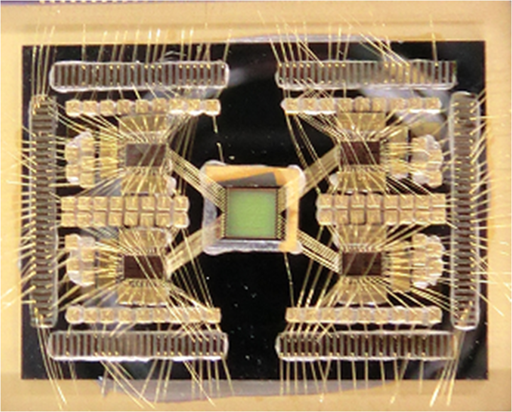 The RID was fabricated in the same SiGe-BiCMOS process with that of the receiver IC. The configuration is basically the same as the one reported in the past literature.12 A photograph of the RID is shown in Fig. 8. A dynamic range of an input voltage of the RID is more than 40 dB. The RID has enough responsiveness to the short pulse of which the width is 1 ns. 5.Evaluation about Range Dependence of the Received SignalWe show an evaluation result about range dependence of the received signal for quantitative demonstration of the developed prototype model. The received optical power of the backscattered light from the target is expressed by the following equation: where is the received optical power (W), is the pulse energy (J), is the pulse width (s), is the aperture diameter of the receiving optics (m), is the distance from the sensor to the target (m), is the transmitting efficiency, which includes various optical power losses in the transmitting process, is the efficiency in the receiving process, is the reflectance of the diffuse hard target, and is the attenuation coefficient of the atmospere. The received voltage is calculated using the following equation: where is the received voltage (V), is the photosensitivity of the APD (), is the avalanche gain of the APD, and is the trans-impedance gain of the TIAs ().We experimentally evaluated the range dependence of the received signal of the prototype model. Table 1 shows the value of parameters in the experiment. The avalanche gain was set to be a low value of 3 on purpose. This was just for this experimental evaluation. Figure 9 shows the experimental and calculated results of the range dependence of the received voltage signal, where the attenuation of the atmospheric propagation is negligible. The experimental result was in good agreement with the calculation result in the range from 20 to 30 m. We consider that the difference at a range of 15 m might be caused by increasing the trans-impedance of TIAs in the receiver IC by the large current input from the high-aspect APD array. The TIAs are made unstable by the large current input. Increasing trans-impedance of the TIAs at a particular frequency might occur by the instability of the TIAs. Table 1Parameter of each component at the experiment.
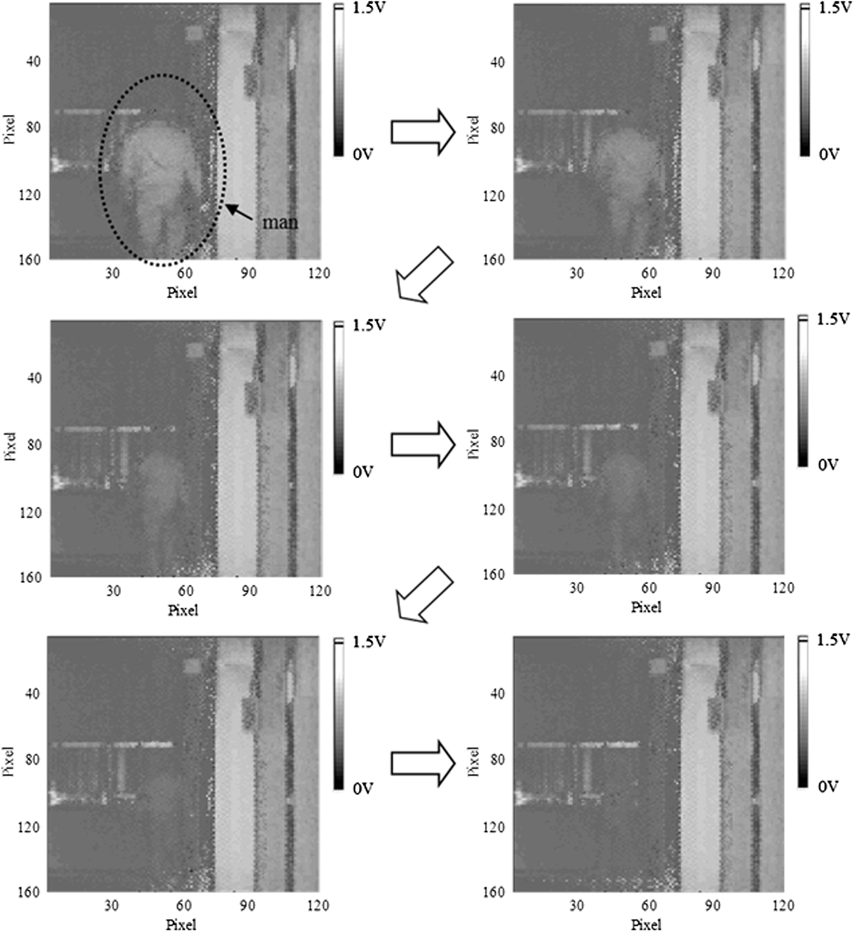
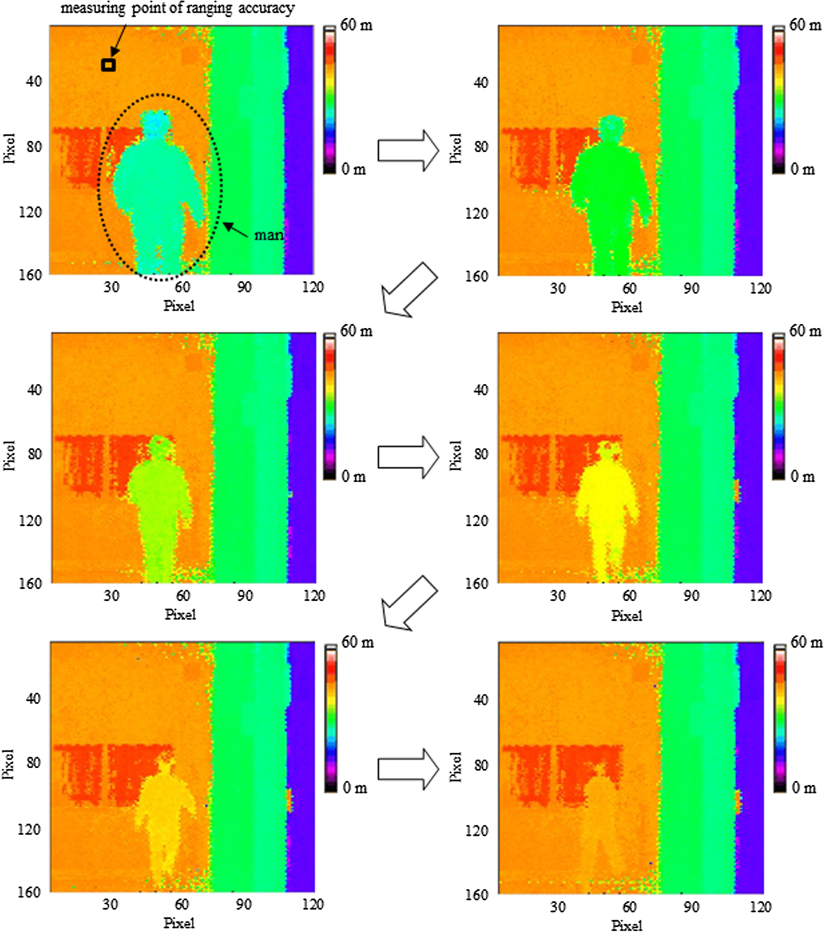
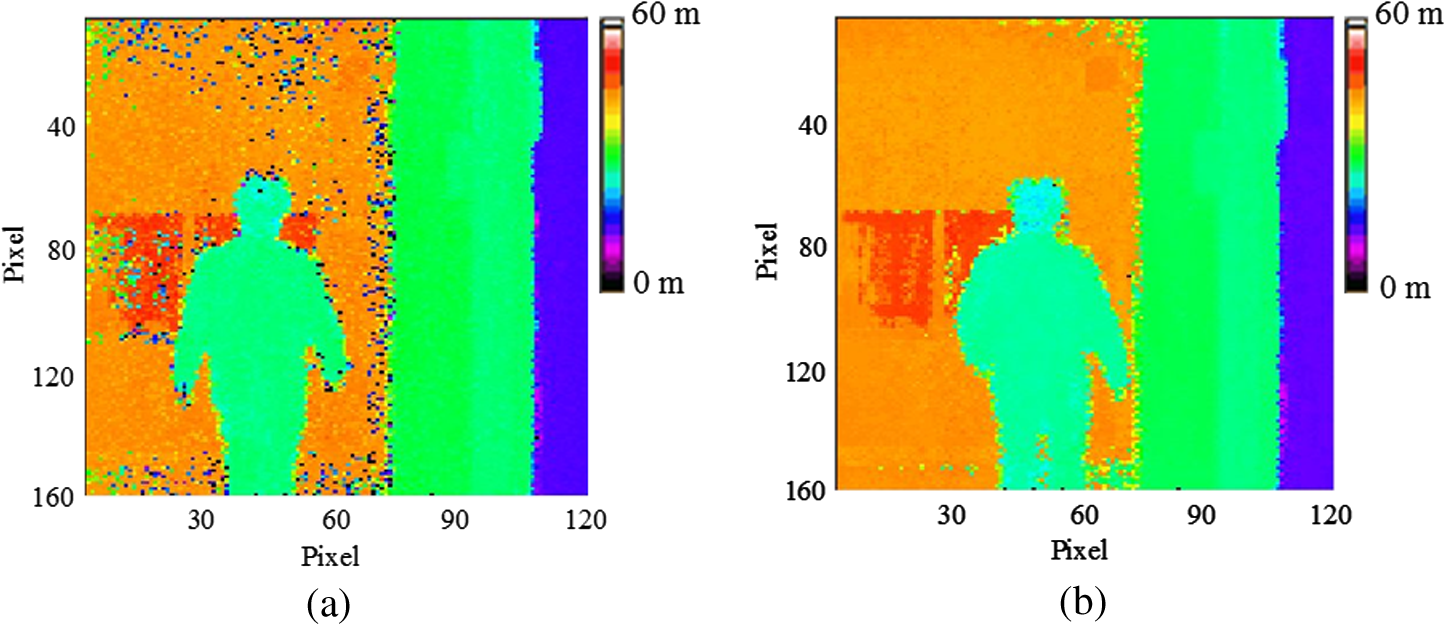
6.Imaging ExperimentWe demonstrated the imaging experiments using the prototype model. The frame rate was 8 Hz for the imaging of . The avalanche gain of the high-aspect APD array was set at 10 in this experiment. Figures 10 and 11 show the imaging experimental results of a man walking. Figure 10 shows the intensity images, which show the intensity of the backscattered light. Figure 11 shows the range images, which show the range from the sensor to the target. The range of scenes in Figs. 10 and 11 is from 20 to 50 m. The measurable TOF width was set at the value corresponding to 50 m. The ranging precision was about 4 cm at the longest range point in Fig. 11. Clearly, this system obtains the range images and the intensity images of the man walking in these figures. Figure 12 shows the noise reduction effect of the SSD in the range images. Figure 12(a) shows that some false detections in the range image appear without the SSD operation. These false detections are caused by the increase of the noise level in the received signal. On the other hand, Fig. 12(b) shows the better range image without false detection by using the SSD. 7.ConclusionWe showed the concept of the range imaging pulse laser sensor with 2-D scanning of a transmitted beam and scanless receiver using a high-aspect APD array for the eye-safe wavelength. This sensor can realize the high frame rate and long-range imaging with the relatively simple sensor configuration. We developed the high-aspect APD array, the receiver IC, and the RID. By combining these devices, we realized a range imaging with a frame rate of 8 Hz at the distance of about 50 m. Furthermore, we demonstrated the noise reduction effect in the range imaging by using the SSD contributing to the long-range imaging. ReferencesR. A. Jarvis,
“A perspective on range finding techniques for computer vision,”
IEEE Trans. Pattern Anal. Mach. Intell., PAMI-5 122
–139
(1983). http://dx.doi.org/10.1109/TPAMI.1983.4767365 ITPIDJ 0162-8828 Google Scholar
D. C. Carmer et al.,
“Laser radar in robotics,”
Proc. IEEE, 84 299
–320
(1996). http://dx.doi.org/10.1109/5.482232 IEEPAD 0018-9219 Google Scholar
R. Stettner et al.,
“Three dimensional flash ladar focal planes and time dependent imaging,”
Int. J. High Speed Electron. Syst., 18 401
–406
(2008). http://dx.doi.org/10.1142/S0129156408005436 IHSSEF 0129-1564 Google Scholar
J. C. Dries et al.,
“A flash laser radar system incorporating InGaAs PIN and APD detectors,”
Proc. SPIE, 5412 250
–256
(2004). http://dx.doi.org/10.1117/12.542609 PSISDG 0277-786X Google Scholar
M. Vaidyanathan et al.,
“High performance ladar focal plane arrays for 3D range imaging,”
in Proc. IEEE Aerospace Conf.,
1776
–1781
(2004). http://dx.doi.org/10.1109/AERO.2004.1367957 Google Scholar
P. Yuan et al.,
“ Geiger-mode ladar camera,”
Proc. SPIE, 7684 76840C
(2010). http://dx.doi.org/10.1117/12.851525 PSISDG 0277-786X Google Scholar
E. Borniol et al.,
“Active three-dimensional and thermal imaging with a pitch HgCdTe avalanche photodiode focal plane array,”
Opt. Eng., 51
(6), 061305
(2012). http://dx.doi.org/10.1117/1.OE.51.6.061305 Google Scholar
E. Garcia et al.,
“Low-cost three-dimensional vision system based on a low-power semiconductor laser rangefinder and a single scanning mirror,”
Opt. Eng., 40
(1), 61
–66
(2001). http://dx.doi.org/10.1117/1.1331267 Google Scholar
D. Inoue et al.,
“Improvement of highly sensitive lidar with a thumb-sized sensor-head built using an optical fiber preamplifier,”
Proc. SPIE, 8379 83790X
(2012). http://dx.doi.org/10.1117/12.920596 PSISDG 0277-786X Google Scholar
C. Niclass et al.,
“Design and characterization of a single-photon imager in CMOS for a MEMS-based laser scanning time-of-flight sensor,”
Opt. Express, 20
(11), 11863
–11881
(2012). http://dx.doi.org/10.1364/OE.20.011863 OPEXFF 1094-4087 Google Scholar
R. Moss et al.,
“Low-cost compact MEMS scanning LADAR system for robotic applications,”
Proc. SPIE, 8379 837903
(2012). http://dx.doi.org/10.1117/12.919804 PSISDG 0277-786X Google Scholar
S. Kameyama et al.,
“3D imaging LADAR with linear array devices; laser, detector, and ROIC,”
Proc. SPIE, 7382 738209
(2009). http://dx.doi.org/10.1117/12.836888 PSISDG 0277-786X Google Scholar
E. Yagyu et al.,
“Design and characteristics of guardring-free planar AlInAs avalanche photodiodes,”
J. Lightwave Technol., 27
(8), 1011
–1017
(2009). http://dx.doi.org/10.1109/JLT.2008.2004954 JLTEDG 0733-8724 Google Scholar
BiographyHidenobu Tsuji received his BS and MS degrees in physics from Tokyo Institute of Technology in 2004 and 2006, respectively, and his PhD in science from Tokyo Institute of Technology in 2011. He is a head researcher at Mitsubishi Electric Corporation. His current research interests include optics in laser sensors and laser sensor systems. Masaharu Imaki received his DE degree from the University of Fukui in 2005. He has been involved in the development of Doppler lidar, Raman lidar, differential absorption lidar (DIAL), and high spectral resolution lidar at the university. In 2007, he joined Mitsubishi Electric Corporation. His current research involves distance imaging sensors, DIAL, and Doppler lidar. He is a member of SPIE, the Japan Society of Applied Physics, the Laser Society of Japan, and the Institute of Electrical Engineers of Japan. Nobuki Kotake received his DE degree from Nagoya University in 2007. Since 2007, he has been with the Mitsubishi Electric Corporation, and he started the development of laser remote sensing systems. His current research involves coherent Doppler lidar and range imaging laser sensors. He is a member of the Institute of Electronics, Information, and Communication Engineers (IEICE) and the Meteorological Society of Japan. Akihito Hirai received his ME degree from Chiba University in 2007. In 2007, he joined Mitsubishi Electric Corporation, where he has been engaged in research and development of silicon microwave monolithic integrated circuits at RADAR and Communication Systems. He is a member of the Institute of Electrical and Electronics Engineers (IEEE) Microwave Theory and Techniques Society and is a member of the IEICE. Masaharu Nakaji received his BS and MS degrees in electronic engineering from Nagoya Institute of Technology College, Nagoya, Japan, in 1999 and 2001, respectively. In 2001, he joined Mitsubishi Electric Corporation, Hyogo, Japan, where he has been engaged in the research and development on high-speed photodetectors. Shumpei Kameyema received his DE degree from Chiba University in 2011. Since 1995, he has been with Mitsubishi Electric Corporation, and he started the development of laser remote sensing systems in 1999. His current research involves coherent Doppler lidar, DIAL, and range imaging laser sensors. He is a member of the Japan Society of Applied Physics, Optical Society of America, and IEEE. |