
|
|
1.IntroductionIn recent years, silicon photonics has been paid great attention for a growing number of applications (e.g., optical communication, manufacturing, biotechnology, energy, etc.) due to its tremendous versatility.1 The silicon photonics is commonly regarded as a promising solution for next-generation optical networks in terms of the low cost, high-refractive index contrast, and compatibility with mature complementary metal-oxide-semiconductor technologies.2 The optical power splitter is a key component for splitting light in optical communication networks.3,4 In a silicon photonic circuit, power splitters are based on typical structures such as a microring,5 directional coupler,6 Y-branch,7 and multimode interference (MMI) coupler.8 Compared with the other structures, the MMI-based optical power splitter has the advantages of low excess losses (ELs) and crosstalk,9 a wide optical bandwidth,10 a compact size,11 and large fabrication tolerances.12 Thus, it is the ideal structure to realize the power splitting function. On the other hand, the reconfigurable functions are highly desired for the next-generation optical communication networks.13 Fortunately, the optical power splitters can sufficiently offer us reconfigurable functionality and introduce further flexibility. The MMI-based optical power splitter is very suitable for achieving the reconfigurable function,14,15 which may derivate novel integrated and compact photonics.16 By designing the MMI structure and modulating the refractive index of specific multimode (self-images) areas, the phase shifts in the MMI coupler can be accurately controlled,17–19 and different splitting ratios at the output ports can then be realized. There are generally two mechanisms to modulate the phase shifts in silicon photonics: current-injection tuning18 and thermal tuning.20 The current-injection tuning scheme is a great option that satisfies the need for a high-tuning speed.21 However, this scheme uses a complex excess doping process, which makes the fabrication more complex.22 Moreover, a doping process with different types and dopant concentrations will introduce more ELs. Therefore, the thermal tuning scheme is preferred to achieve the desired phase shifts on the client side without the need for a high-tuning speed. To improve the thermal tuning efficiency, investigators have still been making continuous efforts to work on developing advanced methods such as using optimized heaters23 and waveguides with optimized thermal isolation structures.24 In this paper, a thermally tuned silicon-based three-channel reconfigurable MMI optical power splitter with four optimized thermal isolations is proposed. To fulfill specific reconfigurable functions (, , and MMI splitters), the optimum geometry of the heaters, desired refractive index changes, and phase shifts of the MMI splitter are designed at first by using the beam propagation method (BPM). Next, the temperature distributions of the devices with and without the thermal isolations are calculated by using the finite element method (FEM) with the appropriate heating powers. By varying the geometry of the thermal isolations, thermal crosstalk between adjacent heaters is observed; meanwhile, the influence of thermal isolation geometry on the thermal crosstalk is examined. Finally, the geometry of the thermal isolations is optimized to ensure high-thermal efficiency (i.e., low-power dissipation) and good optical outputs (e.g., low losses and crosstalk, good uniformity, etc.). 2.Device Structure and Basic MechanismsThe proposed thermally tuned reconfigurable optical power splitter is composed of one multimode waveguide connected to one input port and three output ports, as shown in Fig. 1. The waveguide structure (ridge waveguide) can be fabricated by electron beam lithography (EBL) and inductively coupled plasma (ICP) etching. A silica upper cladding layer (can be deposited on the silicon waveguide structure) and lower cladding layer are fashioned to the MMI coupler, as shown in Fig. 1(a). This structure is located on a silicon substrate. Figures 1(b) and 1(c) show the device’s internal structure without the thermal isolations for clearer visualization, while Figs. 1(d) and 1(e) give similar drawings of the device with thermal isolations consisting of material with low-thermal conductivity (i.e., silica in this study) to increase the thermal tuning efficiency. Since the etching depth of the trenches is the same as the thickness of the MMI, we can realize these thermal isolations by etching some trenches on the MMI structure, until to the oxide layer (), at the same time with the fabrication process of the MMI waveguide structure by EBL and ICP etching. In these figures, the reference lines I′, II′, and III′ are marked to help in the analysis of the temperature distributions of specific thermal tuning areas. These lines go across the MMI couplers along the -axis direction and are just beneath the heaters. Fig. 1(a) Geometric schematic of the thermally tuned MMI coupler. (b) Geometric schematic of the MMI without thermal isolations with the silica upper cladding removed and (d) with four thermal isolations. (c, e) Cross-sections of the MMI corresponding to (b) and (d).  Figure 2(b) describes the prototype of the MMI coupler, which is based on a MMI: without affecting the functions, the input waveguides , and and the output waveguides and are removed to reduce the crosstalk between each channel. Four titanium heaters are designed at specific positions (marked I–IV): above the silica upper cladding. Then the refractive index of the Si multimode waveguide beneath the heaters can be modulated by the thermo-optic effect. We achieve desired phase shifts to fulfill certain functions by heating these specific thermal tuning areas (I–III is at and IV is at ), as shown in Fig. 2(b). Based on the self-imaging theory,17 the effective width and beating length of the two lowest-order modes can be defined as where is the width of multimode waveguide, is the effective width considering the lateral penetration depth of each mode field ( for transverse electric (TE) modes and for transverse magnetic modes), is the input wavelength (set to 1550 nm in this study), and are the effective refractive indices of the multimode waveguide (silicon) and lateral cladding material (silica), respectively, and and are the propagation constants of the zeroth and first lateral modes, respectively. For simplicity, we consider only the situation for TE modes; thus, .Fig. 2(a) Schematic diagram of a thermally tuned MMI coupler. (b) Layout of the device in our study: the thermal tuning areas and thermal isolation positions are marked. 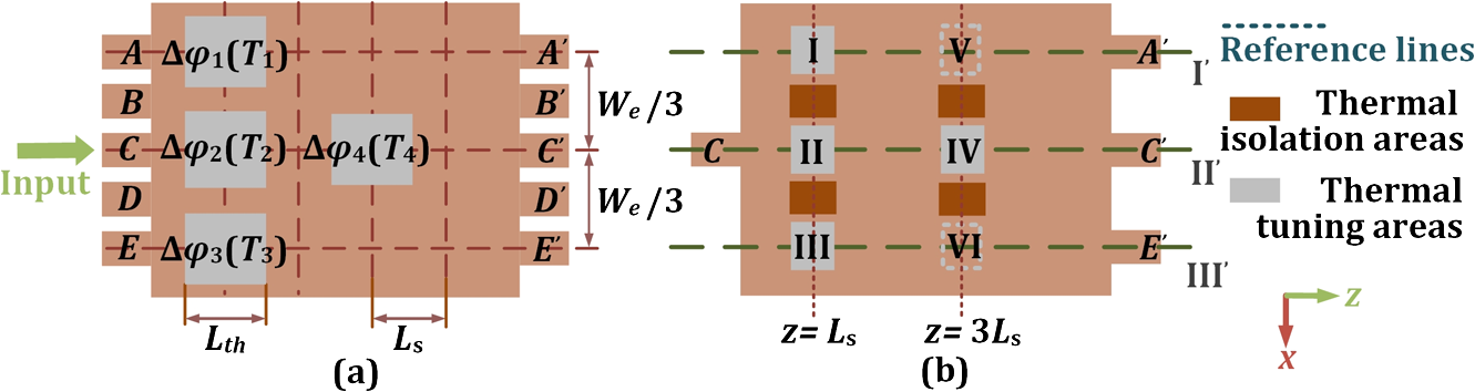 The general matrix theory of self-imaging in MMI couplers with single-mode input and output waveguides is used,18,25 and the multimode waveguide is split into five subsections with the same length , as shown in Fig. 2(a). This is the shortest length for a theoretically lossless MMI coupler: thus, the length of the MMI coupler . In the multimode waveguide of the MMI coupler, if the phase shifts caused by the thermo-optic effect are taken, the complex image amplitudes in the output guides from the complex object amplitudes in the input guides can be described as where is the transfer matrix of complex image amplitudes in each subsection with , and the diagonal matrices and can describe the phase shifts at those specific thermal tuning positions (I–IV). The corresponding equations are as follows: where () are the shifted phases of corresponding I–IV thermal tuning areas.In the proposed reconfigurable three-channel optical power splitter, the output power in each port is thermally tunable, providing three reconfigurable functions: , , and optical power splitter. To achieve these functions, the desired phase shifts of the I–IV thermal tuning areas are easily calculated based on Eqs. (4) and (5): Then the thermally induced refractive index change can be introduced to achieve these phase shifts: where is the phase shift caused by thermal tuning, is the wavelength number, is the thermally induced refractive index change, and is the length of the thermal tuning section. is approximate to the length of the Ti heater . is the refractive index derivative with regard to the temperature (unit: ), and is the temperature difference between the triple self-images located in the thermal tuning areas (I–III or IV–VI) with the same -coordinates ( or ).To obtain the temperature distribution, the following thermal conduction equation needs to be solved: where () is the space coordinates, is the temperature, is the time, and is the heat generation rate defined as the heat generation power for a unit volume. The static form of the thermal conduction equation is where () is the heating power and is the volume of each heater.In this study, material properties such as the density (unit: ), specific heat (unit: ), and thermal conductivity () are regarded as temperature-independent and are listed in Table 1. The initial geometric parameters of the device are listed in Table 2. Table 1Material properties used in the simulation (λ0=1550 nm, T=Tambient=300 K). Note: [MLC] refers to the Material Library in the COMSOL Multiphysics software. Table 2Initial geometric parameters of the device for simulation (unit: μm).
Note: W, L, and H represent the width, length, and height (or thickness) of each component. The subscript wg refers to the single-mode waveguide, c refers to the silica cladding, sub refers to the silicon substrate, and h refers to the heater. 3.Simulation and OptimizationFour thermal isolations in specific positions are designed in the thermally tuned reconfigurable MMI power splitter to boost the thermal tuning efficiency. Meanwhile, to ensure good outputs, some parameters are needed to be optimized such as the heater geometry, heating powers, and thermal isolation geometry. For these complex analyses, taking the thermal-optic effects into account, the temperature distributions and the optical output characteristics of the proposed structure are simulated and analyzed then. We initially set the length of the heater to , similar to Rosa et al.20 Naturally, for a MMI power splitter, temperature rises of the thermal tuning areas (I and II) in the MMI are needed to get corresponding refractive index change , which leads to a phase shift. For the MMI power splitter, and are needed to get and , which leads to and phase shifts at thermal tuning areas II and IV, respectively. However, the geometry of the heater will affect the output characteristics of the MMI coupler, especially for the insertion loss (IL) and the excess loss (EL). To choose the appropriate geometric parameters of the heater, we first considered the situation for the MMI power splitter: the width of the heater is chosen to obtain the minimum IL of the output port with the value 0.288 dB, while as depicted in Fig. 3(a). Based on the contour diagram of in Fig. 2(b), if is set to the optimum value of , and can then be optimized to 51 and , respectively. In this case, the EL can be as low as 0.248 dB, and the crosstalk of the output ports ( and ) can be less than (not the minimum but acceptable). Fig. 3(a) IL of the output port () depending on when is changed (). (b) Contour diagram with when is (in the case of MMI power splitter). 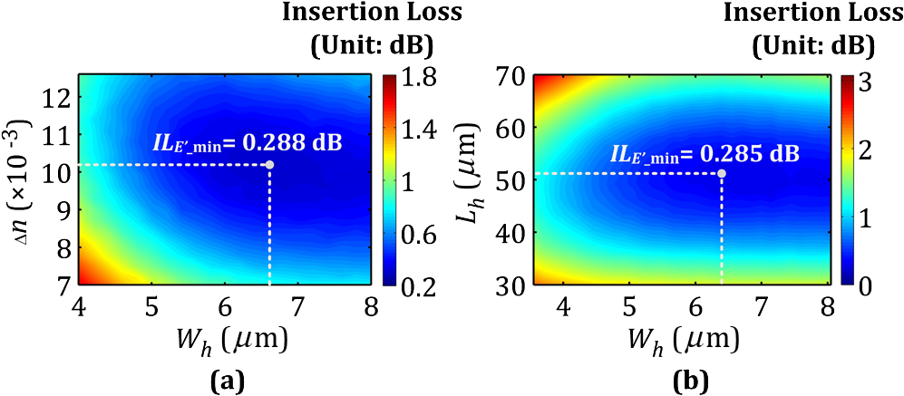 By using the same method for the MMI power splitter, and can be optimized to 51 and , respectively, while and . The EL would be as low as 0.324 dB, the crosstalk of and would be less than , and the uniformity of the output ports and would be better than . For the MMI power splitter, the heater geometry would have a much smaller influence on the output characteristics of the MMI coupler than in the other two cases because there is no thermally induced phase shift. When and are set to 51 and , respectively, the EL is as low as 0.144 dB, and the uniformity of the output ports , , and is better than . Considering all these factors, the geometric parameters of the heater are finally optimized to and . As known the desired phase shifts and thermally induced refractive index changes in these different cases, we can then determine the desired heating powers of the heaters and corresponding temperature rises in the specific thermal tuning areas by sweeping the heating powers with a power step of 0.1 mW. For the MMI power splitter, when the heating powers of heaters I and II are and , the temperature difference between the specific areas (II and III on the reference lines II′ and III′ with ) reaches , and the accumulated phase shift is about . For the MMI power splitter, when the heating powers of heaters II and IV are, respectively, and , the temperature differences between the specific areas (I and II on the reference lines I′ and II′ with and V and IV on the reference lines I′ and II′ with ) reach and 20.7 K, respectively, and the accumulated phase shifts are about and , accordingly. By incorporating the above thermally induced refractive index changes and phase shifts into our simulation, we finally obtain the optical power distributions of the silicon-based three-channel optical power splitter at 1550 nm, as shown in Fig. 4. Fig. 4Optical power distributions of the silicon-based three-channel optical power splitter at 1550 nm: (a) , (b) , and (c) MMI power splitters. 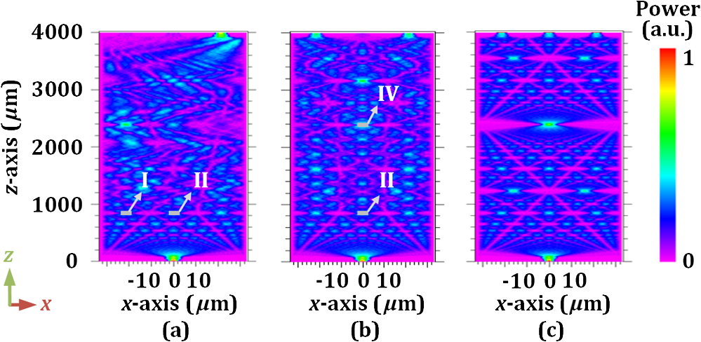 Next, thermal isolations are further added to the designs of the three MMI power splitters discussed above. Detailed thermal simulations are performed by using FEM to analyze the temperature distributions and thermally induced phase shifts. The thermal effects are considered to finally calculate the outputs of the devices based on BPM. Compared with the MMI power splitters without thermal isolations, the optimized device has much higher thermal efficiency and much lower heating power consumption. It should be noted, however, that the influences of the thermal isolation geometry on the device outputs should not be ignored. There is a trade-off between the thermal tuning efficiency and optical outputs. First, the positions of the thermal isolations are needed to be optimized, in order to minimize the impact on the device outputs in terms of excess loss, which is found to be located where the optical field is weak enough. Thus, the best positions are located just in the middle of the adjacent thermal tuning areas with the same -coordinate ( or ), as shown in Fig. 2(b). Figure 5(a) shows the optical power distribution of the MMI power splitter with thermal isolations (, ) at an input wavelength of 1550 nm. This figure clearly shows the thermal isolations. Similar to the case without thermal isolations, the desired refractive index changes are incorporated into our simulation, and the EL is then examined when the geometry of the thermal isolation is varied ( to , : 0.5 to ). It is clear that a smaller isolation area would benefit a smaller EL of the splitter. However, to compromise the trade-off between the thermal tuning efficiency and the optical outputs, we need to choose the optimum geometry parameters of the thermal isolation area. Fig. 5(a) Optical power distribution of the MMI power splitter with thermal isolations at 1550 nm. (b) ELs of the power splitter when the geometry of the thermal isolation changes for MMI power splitters. 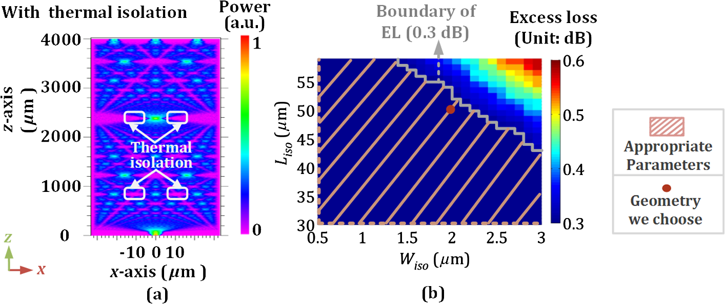 We assume that the EL of less than 0.3 dB is acceptable, as shown in Fig. 5(b). We then draw a reference line (boundary line) to facilitate our observation. The shadow triangle with a reference indicates the region for appropriate parameters, and the red point is corresponding to the geometry parameters we choose. Similarly, for the and MMI power splitters (these two cases are with thermal effects), the EL is also calculated in detail for different geometric parameters of the thermal isolations (: 35 to , : 0.5 to ). For the cases and MMI power splitters, we assume that EL of less than 0.4 dB is acceptable in these two cases. To optimize the geometry of the thermal isolations, the appropriate region is further examined. For the MMI power splitter, the heating powers of heaters I and II ( and ) are both set to 12 mW, and three design geometries of the isolations are studied: (, ) = (, ), (, ), and (, ). Figure 6 shows the one-dimensional temperature distributions of the reference lines [corresponding to lines I′–III′ in Fig. 2(b)] and the temperature differences between these lines. Based on the temperature distributions in Figs. 6(a), 6(c), and 6(e), the temperatures of lines I′ and II′ increase and become close to equal when the size of the isolation is increased. Meanwhile, the temperatures of line III′ decrease obviously. The trend of the temperature changes shows that the influence of thermal crosstalk gradually decreases when the size of the isolation is increased. In more detail, based on the changes in the temperature differences described in Figs. 6(b), 6(d), and 6(f), the heat from the heater clearly seems to be “blocked” by the thermal isolations. Figure 6(f) shows that the temperature differences of (I′–III′) and (II′–III′) are clearly much closer (even equal) compared with those in Fig. 6(b). Therefore, we infer that the thermal crosstalk between each adjacent heater can be eliminated if the geometry of the thermal isolation is large enough, and we set and as our final geometric parameters of the isolations. The fabrication tolerance of our device is concerned in practice, and estimated value is about (the EL changes are within ). Fig. 6For the MMI power splitter, one-dimensional temperature distributions of the reference lines [corresponding to lines I′–III′ in Fig. 2(b)] and the temperature differences between these lines if : (a, b) , ; (c, d) , ; and (e, f) , . 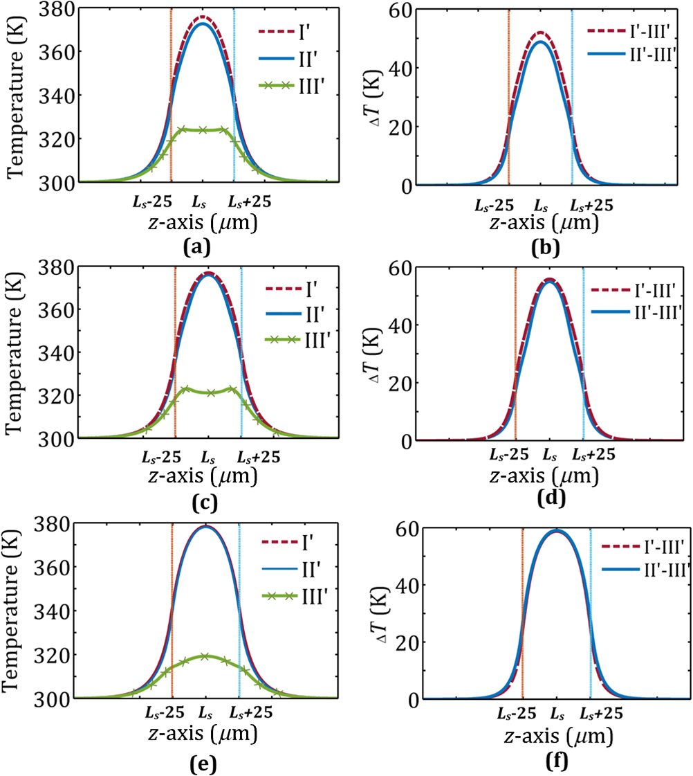 Improvements on thermal tuning efficiency with the thermal isolations are demonstrated with the simulated results in Fig. 7. Figures 7(a), 7(d), and 7(g) show the two-dimensional temperature distributions on cross-sectional drawings ( axis) of the and MMIs without and with the silica trench. In the optimized device, the heating power of the heaters is as follows. For the MMI, (compared with those used in MMI without thermal isolations, the power dissipations are reduced by 25.3% and 43.7%, respectively). For the MMI, and (compared with those used in the MMI without thermal isolations, the power dissipations are reduced by 52.2% and 55.2%, respectively). Figures 7(b), 7(e), and 7(h) present the temperature differences. For the MMI, the maximum temperature difference reaches 58.7 K. For the MMI, reaches 38.3 K (heating by heater II) and 22.8 K (heating by heater IV), respectively. The final accumulated phase shifts are then obtained as shown in Figs. 7(c), 7(f), and 7(i): , , and for the , , and MMI power splitters, respectively. However, it should be noticed that the desired temperature rises of the MMI power splitter with thermal isolations are slightly greater than those without thermal isolations because the isolations reduce the temperature difference more markedly at the edges of the heater [see Figs. 7(b), 7(e), and 7(h)]. Thus, the effective thermal tuning areas [below the curves and above the -axis, as shown in Figs. 7(b), 7(e), and 7(h)] of the MMI power splitter with thermal isolations will be slightly smaller if the desired temperature rises are set to the same value. Fig. 7(a, d, g) Two-dimensional temperature distributions along the cross-section ( axis) of the and MMIs without and with silica trenches. (b, e, h) Maximum temperature difference for and MMIs, respectively. (c, f, i) Final accumulated phase shifts for the and MMIs, respectively. 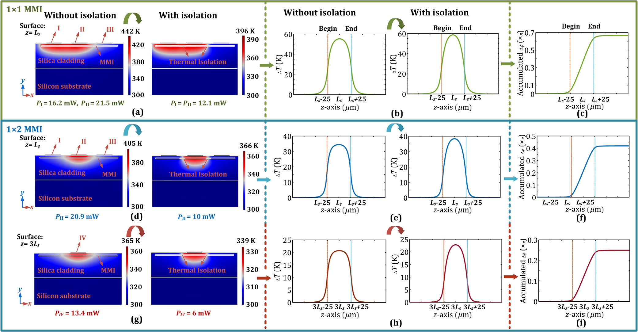 Finally, we obtained the optical power distributions of the optimized , , and MMI power splitters at 1550 nm, as shown in Fig. 8. For the MMI power splitter, the EL is as low as 0.365 dB and the crosstalk of and is less than . For the MMI power splitter, the EL is as low as 0.388 dB and the crosstalk of and is less than . The uniformity of the output ports and is better than . For the MMI power splitter, the EL is as low as 0.272 dB and the uniformity of the output ports , , and is better than . Table 3 compares the final outputs with regard to the cases without and with thermal isolations. It clearly shows the improvements with our design. Fig. 8Optical power distributions of the optimized MMI power splitters at 1550 nm: (a) , (b) , and (c) MMIs. 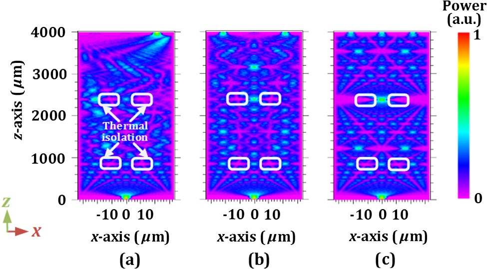 Table 3Results of the outputs without and with thermal isolations.
4.ConclusionIn this paper, we have proposed a thermally tuned silicon-based three-channel reconfigurable MMI optical power splitter with four optimized thermal isolations. The specific and flexible reconfigurable functions (, , and MMI splitters) are achieved by thermally tuning the heaters. By using BPM, the optimum geometry of the heaters, the desired refractive index changes, and phase shifts of the MMI splitter are calculated at first. Next, the temperature distributions of the devices without and with the thermal isolations are analyzed by using FEM. Thermal crosstalk between adjacent heaters is observed by comparing the temperature changes with regard to different geometries of the thermal isolations. We find that the thermal crosstalk between adjacent heaters can clearly be eliminated if the thermal isolation has sufficiently large geometry. To compromise the trade-off between the thermal tuning efficiency and optical output quality, the geometry of the thermal isolation is optimized to and . With the optimum parameters, a high-thermal efficiency (the maximum power dissipations for the and MMI splitters are reduced by 43.7% and 55.2%, respectively) and good optical output characteristics (the maximum EL values are as low as 0.365, 0.388, and 0.272 dB for the , , and MMI splitters, respectively; the crosstalk is less than and for the and MMI splitters, respectively) have been demonstrated. AcknowledgmentsThe authors acknowledge the support provided by the National Natural Science Foundation of China under Grant 61675073, the National High Technology Developing Program of China under Grant No. 2013AA014503, Fundamental Research Funds for the Central Universities No. 2016YXZD004, and Director Fund of Wuhan National Laboratory for Optoelectronics. ReferencesG. T. Reed and A. P. Knights, Silicon Photonics: An Introduction, John Wiley & Sons, Chichester, UK
(2004). Google Scholar
R. Soref,
“The past, present, and future of silicon photonics,”
IEEE J. Sel. Top. Quantum Electron., 12
(6), 1678
–1687
(2006). http://dx.doi.org/10.1109/JSTQE.2006.883151 IJSQEN 1077-260X Google Scholar
L. Wang et al.,
“Design and fabrication of novel symmetric low-loss optical power splitter,”
J. Lightwave Technol., 32
(18), 3112
–3118
(2014). http://dx.doi.org/10.1109/JLT.2014.2337301 JLTEDG 0733-8724 Google Scholar
L. Zheng and M. Zhu,
“Variable optical power splitter based on slot waveguide,”
Proc. SPIE, 7630 76301D
(2009). http://dx.doi.org/10.1117/12.849384 Google Scholar
E. Peter et al.,
“Active microring based tunable optical power splitters,”
Opt. Commun., 359 311
–315
(2016). http://dx.doi.org/10.1016/j.optcom.2015.09.095 OPCOB8 0030-4018 Google Scholar
S. J. Chang and K. W. Liu,
“Design and analysis of optical coupler with a stable splitting ratio based on cascaded multistage directional couplers,”
Opt. Eng., 51
(9), 094603
(2012). http://dx.doi.org/10.1117/1.OE.51.9.094603 Google Scholar
C. Burtscher and D. Seyringer,
“Influence of waveguide structure on Y-branch splitting ratio,”
Proc. SPIE, 9133 91331I
(2014). http://dx.doi.org/10.1117/12.2050846 Google Scholar
M. Tajaldini and M. Z. M. Jafri,
“The influence of nonlinear modal propagation analysis on MMI power splitters for miniaturization,”
Proc. SPIE, 8789 87890P
(2013). http://dx.doi.org/10.1117/12.2021558 Google Scholar
H. Liu et al.,
“Low-loss waveguide crossing using a multimode interference structure,”
Opt. Commun., 241
(1), 99
–104
(2004). http://dx.doi.org/10.1016/j.optcom.2004.07.008 OPCOB8 0030-4018 Google Scholar
P. A. Besse et al.,
“Optical bandwidth and fabrication tolerances of multimode interference couplers,”
J. Lightwave Technol., 12
(6), 1004
–1009
(1994). http://dx.doi.org/10.1109/50.296191 JLTEDG 0733-8724 Google Scholar
Q. Wong and S. Ho,
“Ultracompact multimode interference design by parallel particle swarm optimization by parallel particle finite-difference time-domain,”
J. Lightwave Technol., 28 1298
–1304
(2010). http://dx.doi.org/10.1109/JLT.2010.2040582 JLTEDG 0733-8724 Google Scholar
J. M. Hong et al.,
“Design and fabrication of a significantly shortened multimode interference coupler for polarization splitter application,”
IEEE Photonics Technol. Lett., 15
(1), 72
–74
(2003). http://dx.doi.org/10.1109/LPT.2002.805803 IPTLEL 1041-1135 Google Scholar
R. Zheng et al.,
“An opto-VLSI reconfigurable broad-band optical splitter,”
IEEE Photonics Technol. Lett., 17
(2), 339
–341
(2005). http://dx.doi.org/10.1109/LPT.2004.840038 IPTLEL 1041-1135 Google Scholar
G. K. Singh and V. Janyani,
“Modeling of a high-performance multimode interference optical switch using reconfigurable image modulated region,”
Opt. Eng., 51
(7), 074006
(2012). http://dx.doi.org/10.1117/1.OE.51.7.074006 Google Scholar
Y. Zhang et al.,
“Splitting-on-demand optical power splitters using multimode interference (MMI) waveguide with programmed modulations,”
Opt. Commun., 281
(3), 426
–432
(2008). http://dx.doi.org/10.1016/j.optcom.2007.09.063 OPCOB8 0030-4018 Google Scholar
A. M. Al-Hetar et al.,
“Multimode interference photonic switches,”
Opt. Eng., 47
(11), 112001
(2008). http://dx.doi.org/10.1117/1.3028349 Google Scholar
L. B. Soldano and E. C. Pennings,
“Optical multi-mode interference devices based on self-imaging: principles and applications,”
J. Lightwave Technol., 13
(4), 615
–627
(1995). http://dx.doi.org/10.1109/50.372474 JLTEDG 0733-8724 Google Scholar
J. Leuthold and C. H. Joyner,
“Multimode interference couplers with tunable power splitting ratios,”
J. Lightwave Technol., 19
(5), 700
–707
(2001). http://dx.doi.org/10.1109/50.923483 JLTEDG 0733-8724 Google Scholar
H. Xin, Q. Fang and C. Wang,
“New type of multimode-interference-type thermo-optic variable optical attenuator,”
Opt. Eng., 43
(11), 2497
–2498
(2004). http://dx.doi.org/10.1117/1.1804391 Google Scholar
Á. Rosa et al.,
“High performance silicon optical switch based on a thermo-optically tunable multimode interference coupler and efficient electrodes,”
Opt. Express, 24
(1), 191
–198
(2016). http://dx.doi.org/10.1364/OE.24.000191 OPEXFF 1094-4087 Google Scholar
A. Liu et al.,
“High-speed optical modulation based on carrier depletion in a silicon waveguide,”
Opt. Express, 15
(2), 660
–668
(2007). http://dx.doi.org/10.1364/OE.15.000660 OPEXFF 1094-4087 Google Scholar
D. A. Mayarrioja and P. Likamwa,
“Tunable multimode interference devices,”
Proc. SPIE, 6243 62430H
(2006). http://dx.doi.org/10.1117/12.669738 Google Scholar
N. C. Harris et al.,
“Efficient, compact and low loss thermo-optic phase shifter in silicon,”
Opt. Express, 22
(9), 10487
–10493
(2014). http://dx.doi.org/10.1364/OE.22.010487 OPEXFF 1094-4087 Google Scholar
X. Han et al.,
“Numerical analysis on thermal tuning efficiency and thermal stress of a thermally tunable SG-DBR laser,”
IEEE Photonics J., 8
(3), 1
–12
(2016). http://dx.doi.org/10.1109/JPHOT.2016.2558042 Google Scholar
J. M. Heaton and R. M. Jenkins,
“General matrix theory of self-imaging in multimode interference (MMI) couplers,”
IEEE Photonics Technol. Lett., 11
(2), 212
–214
(1999). http://dx.doi.org/10.1109/68.740707 IPTLEL 1041-1135 Google Scholar
H. Li,
“Refractive index of silicon and germanium and its wavelength and temperature derivatives,”
J. Phys. Chem. Ref. Data, 9
(3), 561
–658
(1980). http://dx.doi.org/10.1063/1.555624 Google Scholar
Q. Wu et al.,
“Silicon thermo-optic variable optical attenuators based on Mach–Zehnder interference structures,”
Opt. Commun., 341 69
–73
(2015). http://dx.doi.org/10.1016/j.optcom.2014.12.013 OPCOB8 0030-4018 Google Scholar
|


