|
|
1.IntroductionFluorine-doped tin oxide ( or FTO) has demonstrated value as a transparent conducting oxide in solar cells.1,2 It has been suggested as a heat-absorbing coating for window glass.3–5 More recently, FTO has been investigated as a host for surface plasmon polaritons (SPPs) in proposed infrared plasmonic devices.6–8 is a wide band-gap semiconductor with natural n-type conductivity due to oxygen vacancies9 and interstitial Sn.10 Since tin exists in the lattice as an ion with charge , each oxygen atom in the chemical formula accepts two electrons from Sn. Thus, each oxygen vacancy may result in two free electrons. Doping with fluorine is known to increase conductivity, allowing to be used in electronic devices.11,12 Fluorine dopants are initially expected to fill oxygen vacancies, which relieves the surrounding lattice distortion.13 Thus, low-level fluorine doping may actually decrease free-electron density because two free electrons of the vacancy are reduced to one, due to the reception of the other electron by the fluorine to complete the bond. At higher concentrations, F may replace O in the lattice, causing an increase in the carrier concentration. The highest fluorine concentrations may include interstitial fluorine, which is an electron acceptorthat would decrease the free-electron density, as has been observed.13–15 In any case, the electron concentration might be a complicated function of fluorine dopant concentration that depends on the conditions of growth and doping. SPP properties depend on the frequency-dependent complex permittivity, which depends not only on carrier concentration but also on relaxation time (in the Drude model) and on other loss processes in general. The latter properties may depend on physical characteristics such as crystallinity. All relevant quantities may interact in a complex way. Thus, for plasmonic applications, it is important to investigate electrodynamic, transport, and physical properties simultaneously as a function of growth conditions and dopant concentration. Fluorine doping is a means of controlling conductivity, which is necessary for many optoelectronic applications. Specifically, in the case of plasmonics, the free-carrier concentration and mobility have much to do with confinement and propagation of SPPs, which are inhomogeneous electromagnetic waves bound to the surface of a conductor. The frequency at which the real part of the permittivity passes from positive to negative values can be considered to represent the transition point from dielectric to metallic optical behavior. The latter is required to sustain an SPP. The “dressed” plasma frequency is often defined as the frequency corresponding to this zero-crossing frequency.16,17 At lower frequencies, the material is able to support SPPs, where such material may find application in proposed plasmonic devices. Although an investigation of SPPs on transparent conducting oxides (TCO) can be found as far back as 1990,18 interest and activity in TCOs for plasmonics has accelerated strongly within the last decade. Specific TCO-based plasmonic devices have included on-chip waveguides,19 perfect absorbers,20,21 filters,22 and modulators.23 The plasmonic TCOs investigated so far are predominantly indium tin oxide and gallium- or aluminum-doped zinc oxide.24,25 More comprehensive reviews on plasmonic materials can be found in the literature.24–26 Plasmonic applications could benefit from low-cost large area deposition of an environmentally friendly inexpensive material such as FTO. Many approaches to fabrication of FTO have been reported, including pulsed laser deposition,27 sol–gel,28 sputtering,11,12 sintered powders,29 and chemical bath deposition.30 Our approach is an aqueous spray method, which has been shown to give perfectly conformal coatings with plasma frequencies up to the near infrared.6 The perfect conformity is important because many plasmonic applications require structured devices, such as slot waveguides,31,32 transmission gratings, 33 and lamellar gratings.6 There have been several other studies of aqueous spray deposition of FTO with similar chemistry and conditions.15,34–36 These studied electrical properties, optical transparency, and their dependence on F doping and growth conditions, with emphasis on application as transparent conductors. Missing are detailed studies of electrodynamic properties relevant to infrared plasmonic applications, which is the emphasis of this paper. An objective of this study is to determine the range over which the plasma frequency can be tuned by fluorine doping and growth conditions. The plasma frequency is important to plasmonic applications because SPP fields are most tightly bound when their frequency is close to it. 2.Experimental DetailsFTO films were grown on hydrophilic substrates by streaming process for electrodeless electrochemical deposition (SPEED) at atmospheric pressure.7 In contrast to chemical bath deposition, SPEED ensures that films grow by heterogeneous reaction on the surface rather than in solution. Precursors comprised 0.4 M stannic chloride () and ammonium fluoride () dissolved in a mixture of deionized water and organic solvents. Water (20% by volume) acts as a solvent, as the source of the surface-attached nucleation sites for heterogeneous reaction, and as the source of oxygen. The organic solvents ethanol, isopropanol, and methyl propanol serve mainly as complexing agents for Sn ions. For convenience, we chose silicate glass surfaces on which to grow films since these hydrophilic surfaces attach hydroxyl ions to serve as nucleation sites. The ions attract positively charged complexes to initiate the electrochemical reaction, without external electrical field or electrodes. The heterogeneous chemical reactions are where L is the ligand supplied by the organic solvents, [Sub] is the heated substrate, p is the charge of the ligand L, and is the number of ligands involved in the Sn/L coordination. Up arrows indicate decomposition and evaporation of reaction byproducts. Substrate temperature must exceed the heterogeneous reaction activation energy and be sufficient to eliminate byproducts. Site regeneration follows: The freshly attached initiates the next growth cycle. Lateral grain growth competition leads to nanoparticle morphology. Fluorine doping follows:Oxygen vacancies occur via adsorption of the tin complex according to We already demonstrated good nanocrystalline films with plasma wavelength near using 20% F/Sn precursor ratio at growth temperatures near .6 We began this study with a coarse sampling that spanned a wide range of F concentrations at the more moderate temperature 450°C using borofloat glass substrates. Results presented below suggest the need for higher temperatures, so a second set of samples was processed at 480°C, but with finer sampling of the F concentration. Results for this group suggested that even higher temperatures would increase the achieved conductivity. To achieve higher surface temperatures for the same 480°C hot plate temperature, we turned to thinner substrates with higher thermal conductivity, namely silicon, on which a thin hydrophilic layer was first deposited. Silicon substrate is also advantageous with respect to CMOS compatibility. The investigation with silicon substrates focused on the highest doping to achieve the highest conductivity near the limiting temperature of our growth apparatus. All temperatures refer to hot plate temperatures. Measurement of substrate surface temperature would be preferred, but this is impractical. Contact thermometry disturbs the film growth. Infrared thermometry is hampered by poor knowledge of the emissivity and by obscuring clouds of steam during deposition. Table 1 presents the list of the samples prepared and studied for this paper, along with growth temperature, substrate, and nominal fluorine concentration. The latter is the concentration in the precursor solution. The hot-plate exceeds the actual growth temperatures due to imperfect thermal coupling, finite substrate thermal conductivity, and evaporative cooling at the surface. Precursor solutions were mixed with targeted fluorine concentrations. The flow rate through the spray nozzle was set using a manual valve. When changing between solutions with different concentrations, the valve was closed, all lines were cleaned, and the valve was reset to the original position for spraying the next film. Table 1FTO samples.
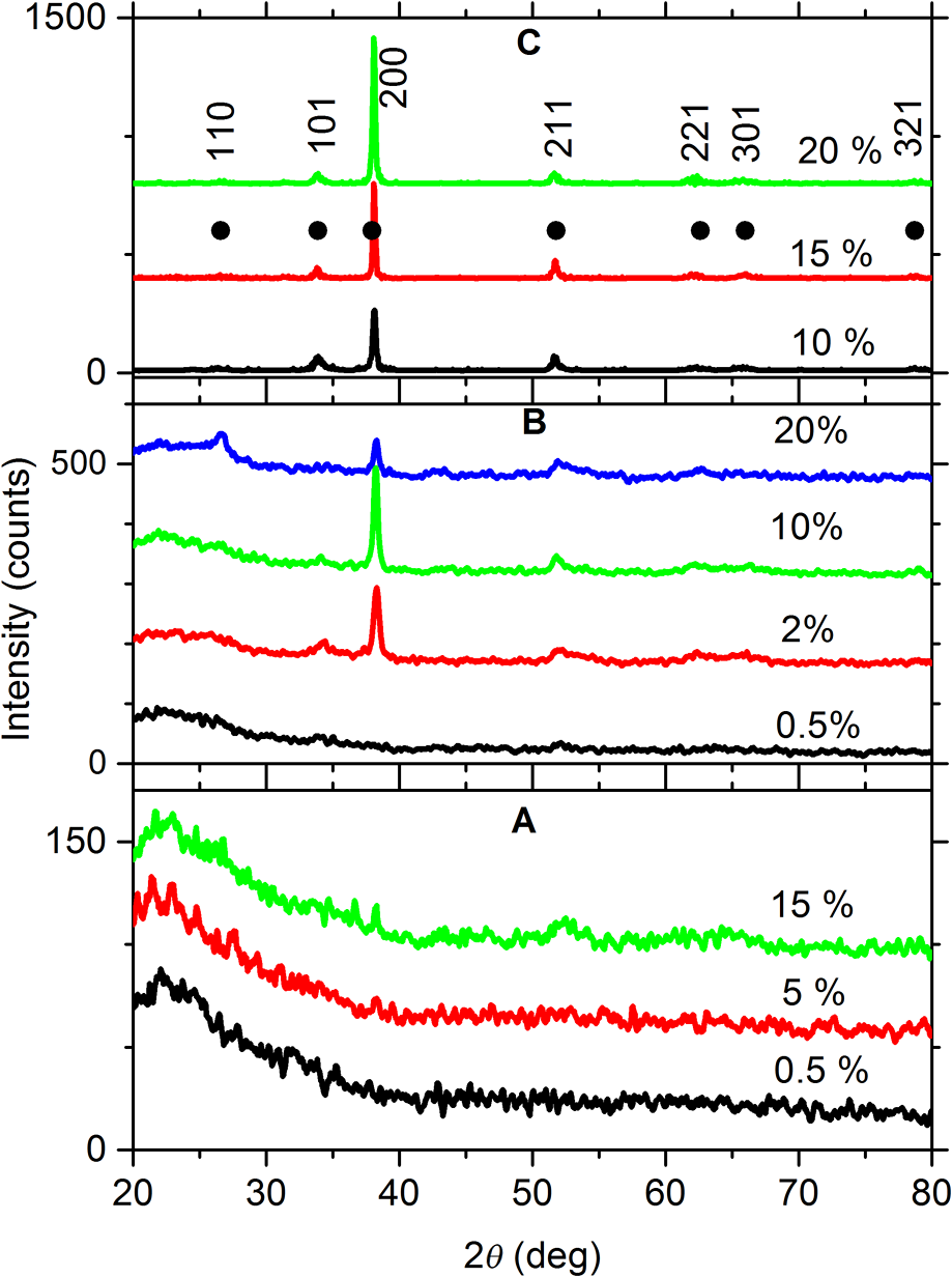
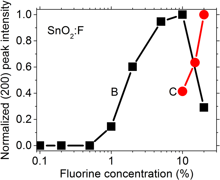
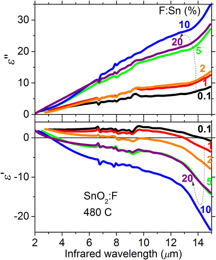
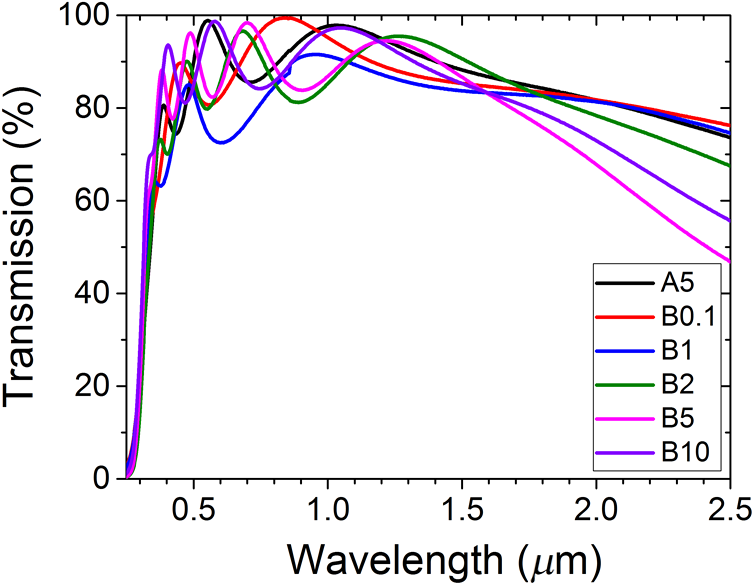
Asymmetric out-of-plane x-ray diffraction (XRD) was performed at fixed incidence using a Cu x-ray mirror with a -deg divergence slit and a 0.04-rad soller slit on the incident beam. The divergent beam also had a 0.04-soller slit and was measured on a PIXcel detector comprising a array. All detectors were used in a scanning line mode to integrate the signal across each line for a cumulative dwell time of 20.4 s per 0.05 deg step over a range of 10 deg to 90 deg. Vertical concentration profiles of Sn, O, F, and Cl were determined using secondary ion mass spectroscopy (Physical Electronics ADEPT 1010 quadrupole SIMS). The primary 3 keV ions were rastered over a area at 45 deg incidence with beam current 20 nA. To reduce the crater side wall effects, a 20% electronic gating was used to collect the ejected ions from just the center region. For the calibration standard, fluorine ions were implanted into an undoped SPEED-grown film at 180 keV energy and ion dose of (Leonard Kroko, Inc.). A sputtering rate of was determined for the implanted standard by crater-depth profilometry. This rate was assumed to hold for the other films when deducing their thicknesses from the SIMS depth profiles. A relative sensitivity factor (RSF) value of was determined from the implant dose and the sputtering rate using SIMetric (the instrument control program), whose three cursors on the interactive display define integration limits and background. Recorded intensities for fluorine were normalized to the Sn intensity from the matrix, and the fluorine concentration [F] of the SPEED-grown films was determined according to . SRIM/TRIM simulation indicates that the dopant concentration peak (ion range) occurs at depth 206.1 nm, but SIMS data for the implanted standard find the peak at a depth of 237 nm, where the peak fluorine concentration was determined to be . The concentration was calculated from the mass density to be , so the peak F/Sn ratio in the standard was 1.12%. Sample thicknesses were determined using cross-sectional imaging with a scanning electron microscope (SEM). SEM images of typical polycrystalline FTO surfaces have been published.6,7 Contactless rf-eddy-current method (Lehighton Electronics, Inc.) was used to map sheet resistance , whose values were also determined by a four-point probe method. Resistivity was found by multiplying and film thickness. Hall effect measurements were completed using an Accent Optical Technologies system in the Van der Pauw configuration. The magnetic field strength was 4.86 kG with the current fixed for each film measurement. The measurements were used to determine carrier type, carrier concentration , and mobility . Resistivity from Hall data was determined according to , where is the electron charge. All films were characterized over the 2- to wavelength range using a J.A. Woollam IR-VASE infrared ellipsometer. For each set of samples, the substrates were first characterized and their complex permittivity spectra used in the subsequent film analysis. Complex optical constants were fitted to a single layer with thicknesses determined by SEM. This method is not necessarily Kramers–Kronig consistent, but it prevents loss of small features such as those observed in the 6- to range, and it retains a measure of the noise. As a check, the layer was also modeled using Kramers–Kronig consistent oscillators; practically the same optical constants were obtained, but the fine details were lost. The ellipsometer beam spot on the samples was roughly elliptical with height 0.3 cm and length 1.2 cm. The elongation was due to the oblique incidence. The spot size exceeds the average dimension of crystallites in the film by a factor of a million, so the measurement represents a large spatial average of the material. The nonuniformity of the permittivity across the samples might be comparable to the observed variations in conductivity and thickness, which were on the order of 12% (see Sec. 3), but these variations within the ellipsometer spot are much lower. Ellipsometry was performed only at the center of each film, where a SEM cross section was used to determine the film thickness. Transmittance spectra over wavelengths from UV to near-IR were collected using a PerkinElmer Lambda 900 spectrometer at ambient conditions. The useful wavelength range was 200 nm to at 2-nm resolution. A spectrum of uncoated borofloat glass was used as reference. Film thicknesses were determined from the average fringe separation in wavenumbers using as the index value for . 3.ResultsFigure 1 shows XRD data for sample sets A, B, and C. Samples A show a broad band at low angles due to the glass substrate. The A samples have no distinct peaks, and only at the highest concentration do some weak broad peaks begin to appear at 53 deg and 64 deg, which are near to the positions of the (211) and (221) peaks for . There is only the barest suggestion of a sharp (200) peak in sample A15. Thus, the A samples appear to be poorly crystallized. Only a selection of the XRD data for the B sample set is presented, but all samples were so characterized. These films show distinct peaks of tetragonal , class , space group on top of the broad substrate band. The 30 deg higher growth temperature compared to A samples evidently improved the crystallinity, but this also apparently depends on the F concentration. The (110) peak of is observed only for sample B20. For samples C, the glass feature is missing and no Si peaks were observed. The (110), (101), (200), (211), (221), (301), and (321) peaks are identified by symbols and labeled (PDF# 000-041-1445). No additional peaks were observed, and the observed lines do not match the reference data for other tin oxides, such as SnO or . The C samples are clearly more crystalline than the other two groups, which we attribute to high growth temperature on the more thermally conducting Si substrates. As for the B samples, the peak heights depend on F concentration. The XRD peak strengths depend systematically on F/Sn ratio. Figure 2 presents the (200) peak height versus nominal [F] concentration for samples B and C. The values have been normalized to the maximum value within each sample set. Except for the highest concentration B sample, the peak intensity increases monotonically with nominal F:Sn ratio, suggesting increased crystallinity with [F]. The observed peak-strength differences cannot be explained in terms of differences in film thickness. As will be shown below, the thickness of the B samples varies nonmonotonically with nominal F concentration by only a factor of , while the change in thickness for C samples (monotonic in SEM data, but nonmonotonic in SIMS data) is by only a factor of 1.2. The decrease in XRD peak strength at the highest F concentration for B samples might be due to the accumulation of fluorine at interstitial lattice sites, which should deform the lattice. That such a decrease does not occur in the C series may be due to the effectively higher surface temperature during growth (if higher temperature favors substitutional over interstitial positions.) The full widths at half maximum of the dominant (200) peak are 0.5 deg and 0.25 deg for samples B and C, respectively, independent of [F]. The Scherrer equation37 gives a lower bound for the mean size of ordered crystalline domains , where is the shape factor, Cu K-alpha wavelength, is in radians, and the Bragg angle is 19 deg. For sample sets B and C, we find the crystalline domains to be not smaller than and 20 nm, respectively. The higher surface temperature during growth for samples C unsurprisingly tends to favor a higher degree of crystallinity and larger crystallite size. Figure 3 presents a plot of the actual F/Sn ratio determined from the analysis of SIMS data for all three sample sets as a function of the ratio in the starting solution. The dashed line with unity slope shows that the achieved F concentration is proportional to the amount added to the solution but lower by a factor of . The values for C samples tend to lie above the line through the values for the B samples. The values for the A samples fall below. Thus, higher growth temperature tends to favor fluorine incorporation into the lattice. The fluorine concentration was observed to be fairly uniform throughout the film thickness for most of the samples. Fig. 3Actual F/Sn ratio as a function of nominal ratio for the three sample sets. The dashed line indicates unity slope.  As an independent confirmation of the SIMS concentration values, sample B20 was measured by x-ray photoelectron spectroscopy (XPS). The fluorine peak was very weak, but long averaging allowed us to determine a fluorine concentration of . This value is close to the value 0.46% for the data point shown in Fig. 3. From XRD data, sample B20 appears to be an outlier, which has been tentatively attributed to lattice deformation caused by an accumulation of interstitial fluorine. However, XPS at this level of signal-to-noise ratio is insensitive to the deformation of the lattice or to the positions of F atoms, so it remains a useful check on the SIMS values. This most heavily doped B sample was the only one that gave sufficiently strong XPS signal to quantify its fluorine concentration with any confidence. C samples were not investigated by XPS. Figure 4 presents a sheet resistance map determined by the contactless method for sample C20. The contours are correlated with the positions of the clips used to hold the substrate in contact with the hot plate during growth. This again shows the importance of substrate temperature on film properties. The average value is with 12% systematic spatial variation over the 5-cm lateral dimension of the film. A similar measurement on sample A15 shows twice higher spatial variations, which is attributed to lower temperature uniformity during growth on this thrice thicker, -less-thermally conductive glass substrate. Figure 5 presents plots of film thickness, resistivity, Hall mobility, and electron concentration as a function of fluorine concentration. Thicknesses determined from SEM imaging and SIMS profiling are presented first in Fig. 5. The SEM and SIMS values are in good agreement. The C samples are more than twice as thick as the A and B samples for the same [F]. We interpret this to be a consequence of the higher growth temperature on Si substrates due to higher thermal conductivity. Fig. 5Thickness, resistivity, mobility, and electron concentration for sample sets A (green), B (black), and C (red) as a function of nominal fluorine concentration. 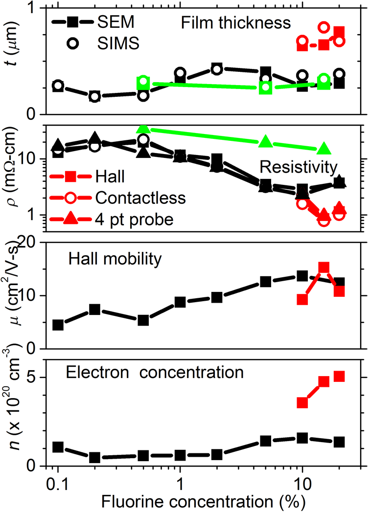 Next, Fig. 5 shows resistivity versus [F]. SEM thickness values were used to determine the plotted values. Hall, contactless, and four-point probe values are in good agreement. Samples A have the highest resistivity, and the values decrease with increasing nominal [F]. For samples B, a 200-fold [F] increase varies the resistivity by only a factor of , and this variation is systematic but nonmonotonic. Set C has overall lower resistivity, with lowest value achieved at . The Hall values of mobility and electron concentration are also plotted in Fig. 5 for samples B and C. For B samples, varies only by a factor of 3.3, while varies by a factor of 3.0, so both factors contribute nearly equally to the observed 10-fold variation in resistivity. Since the mobility values for B and C samples are about the same, their difference in resistivity value is due mainly to their different electron concentrations. The electron and actual fluorine concentrations in sample C20 are and , a difference of only 14%, which is comparable to the level of uncertainty for [F] values from SIMS. A similar situation holds for sample B10. This suggests that a substantial portion of F dopant ions in SPEED-grown films can be electrically active. On the other hand, with decreasing [F], the electron concentration does not drop proportionally. For the lowest doped sample, by a factor of , which suggests an additional source of free carriers, possibly oxygen-vacancy double-donors. The resistivity of the undoped film before ion-implantation was determined by 4-pt probe to be , which is a factor 20 to 750 higher than for the F-doped samples shown in Fig. 5. That means that the doping process during SPEED growth is responsible for all of the additional charge carriers, even if they cannot all be accounted for by the concentration of F. Interestingly, the implanted standard prepared for SIMS had a resistivity of , i.e., higher than that of the undoped film before implantation. This suggests that implant damage substantially worsens the electron mobility and that the implanted F ions are not all electrically active. Thus, ion implantation is a poor approach to preparing FTO, unless a suitable annealing process can be developed to heal the damage and activate the dopants. In any case, SPEED has the practical advantage over implantation of being a low-cost, large-area fabrication process. Figure 6 presents real and imaginary parts of the permittivity spectra in the infrared wavelength range 2 to for different F concentrations (sample set B). The magnitudes of both parts of the permittivity are similar. The increases, and becomes more negative, with increasing F concentration up to 10%, after which the change reverses. The zero crossings of shift to shorter wavelength up to , after which it stops changing. There is structure in the 6- to range. This is not due to the known IR-active phonon bands of (three of type and one of ), which fall in the wavelength range 14 to .38–41 Note particularly the broad peak in at , which is similar to the well-known absorption band in silicates.42 This band becomes weaker with increasing [F]. In A samples grown at 450°C, the overall curves have lower value, and the peak is much stronger while retaining the same weakening trend with increasing [F]. Figure 7 presents plots of the zero-crossing wavelength for the three sample sets (labeled) and also a single data point from the literature.6 The A samples are metallic only at the highest fluorine concentrations, and then they behave optically as conductors only beyond wavelength. The B and C samples have zero-crossings throughout the midwave IR (3 to ) to long-wave IR (8 to ) for all values of F doping studied. At low doping values, the zero-crossings are all about 14 to wavelength. At , the zero-crossing wavelength drops rapidly with increasing concentration until about 5% F, when the value stops changing and remains at about 2 to . Though the changes with [F] in Fig. 6 spectra reverse above 10%, the zero crossings do not. The high-concentration zero-crossing wavelengths for samples B exceed those for samples C by a factor of . Fig. 7Zero-crossing wavelengths for the real-part of the permittivity versus fluorine concentration. 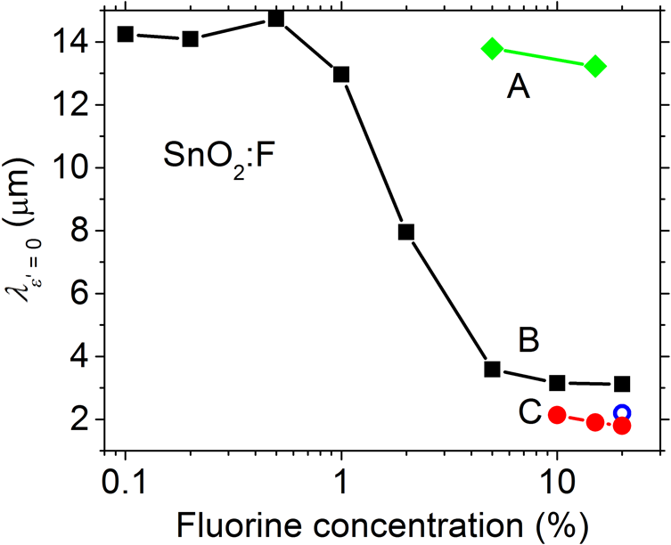 There may well be plasmonic applications such as structured plasmonic resonators that provide wavelength-specific infrared or microwave absorption simultaneously with visible and near-IR transparency. Figure 8 presents examples of UV-visible transmittance spectra of A and B films that confirm such transparency. (The silicon substrates of C films are opaque in this wavelength range.) All A and B films were so characterized and all show similar features. These include fundamental absorption at around 300 nm wavelength (4.1 eV), high transmittance at longer wavelengths, and oscillations due to Fabry–Perot resonances in the films. The latter arise because the index () differs significantly from that of air (1) and borofloat glass (1.47). Film thicknesses determined from the fringes agree with the values plotted in Fig. 5. The longest wavelength transmission decreases within increasing conductivity. For the highest conductivity samples, this down turn happens near the plasma wavelength where the transition from dielectric to metallic optical behavior begins. 4.DiscussionFigure 4 shows the importance of temperature uniformity in obtaining uniform electrical properties of the film. Silicon has more than two orders of magnitude higher thermal conductivity than borofloat glass, and the Si substrates were three times thinner, so the surface temperature should be higher for the C samples. The elevated temperatures volatize and eliminate reaction byproducts that impair conductivity, so C films are expected to have higher quality and higher uniformity. We observe the C samples to be more crystalline, with larger crystallite size, higher electron concentration, and lower resistivity. The thickness oscillations with changes in F concentration are difficult to understand, but the observed nonrandom behavior suggests either a physical interaction or a systematic error due to some uncontrolled environmental factor for samples processed in order of increasing concentration. If the variations were due to uncertainties in the positioning of the manual value on the spray system, one would expect a more random variation in thickness. For sample B0.1, the actual fluorine concentration is , while the free-electron concentration . In undoped grown by SPEED, , assuming its higher resistivity is due mainly to lower free-electron density. These values are inconsistent with a model in which F dopants initially fill oxygen vacancies, replacing those double donors by F single donors and thereby reducing .13 For each F ion in this sample, there are an additional 60 free electrons compared with the undoped . Thus, the very process of F doping in SPEED is introducing electrically active defects far above the actual number of dopant impurities. In contrast, at the highest doping levels, , so all free electrons can be accounted for if the majority of fluorine ions replace oxygen ions in the lattice. Similar to Ref. 15, we see a minimum in FTO resistivity at . However, in contrast to Ref. 15, we do not see a minimum in or a maximum in at this concentration. Rather we observe a monotonic change in from 10% to 20%, and a maximum in . Thus, our resistivity valley at 15% is due to our mobility peak, not a concentration peak. Reference 13 also reported that the highest concentration of F does not give the lowest resistivity, and this was attributed to the appearance of interstitial F when doping is heavy. Permittivity curves for FTO measured out to have been extrapolated to wavelength on the basis of the Drude model.17 These extrapolations have been used to predict SPPs properties in the long-wave infrared. However, our measurements show considerable structure in the 6- to wavelength range, and the magnitude of this structure depends on how the films are prepared. Thus, previously predicted SPP properties based on Drude-model extrapolation are somewhat lacking in confidence. The main objective of this study was to investigate the range over which the plasma frequency could be tuned by fluorine doping and growth conditions. We summarize that we achieved plasma wavelengths from beyond to below . In other words, obtaining plasma frequencies anywhere in the important midwave and long-wave infrared bands was shown to be possible. It is clearly possible to obtain even longer plasma wavelengths into the far-IR and mm-wave regions with FTO, but apparently it would be difficult to go much below in the near-infrared. However, there are many other materials well suited for that range.25,26 5.ConclusionIn conclusion, electrodynamic properties of fluorine-doped tin oxide films grown by aqueous spray deposition were correlated with physical and electrical properties over a broad range of doping concentrations. Results indicate that the substantial reduction in resistivity of doped films with respect to undoped results from a complex mechanism of free-electron generation, which depends on the doping process but is not simply accounted for by the density of dopants. Crystallinity, mobility, and carrier concentration all have complicated dependence on dopant concentration and surface temperature during growth. The results presented here especially inform the tailoring of electrodynamic properties in aqueous-spray grown FTO for application to infrared plasmonics. AcknowledgmentsPeale was partially supported by the AFRL Sensors Directorate as a summer contractor with Wyle Aerospace. AFRL authors were supported by Air Force Office of Scientific Research under AFOSR LRIR No. 15RYCOR162 (Program Officer Dr. Gernot Pomrenke). The authors have no relevant financial interests and no other potential conflicts of interest to disclose for this manuscript. ReferencesM. M. Lee et al.,
“Efficient hybrid solar cells based on meso-superstructured organometal halide perovskites,”
Science, 338
(643), 643
–647
(2012). http://dx.doi.org/10.1126/science.1228604 SCIEAS 0036-8075 Google Scholar
H. Kim et al.,
“Lead iodide perovskite sensitized all-solid-state submicron thin film mesoscopic solar cell with efficiency exceeding 9%,”
Sci. Rep., 2 591
(2012). http://dx.doi.org/10.1038/srep00591 Google Scholar
N. N. Greenwood and A. Earnshaw, Chemistry of the Elements, 447
–448 Pergamon Press, Oxford
(1984). Google Scholar
H. Huang et al.,
“Solvothermal synthesis of nanoparticles and IR shielding coating for smart window,”
Mater Des., 88
(25), 384
–389
(2015). http://dx.doi.org/10.1016/j.matdes.2015.09.013 Google Scholar
F. Khalilzadeh-Rezaie et al.,
“Fluorine-doped tin oxides for mid-infrared plasmonics,”
Opt. Mater. Express, 5
(10), 2184
–2192
(2015). http://dx.doi.org/10.1364/OME.5.002184 Google Scholar
F. K. Rezaie et al.,
“Optical and electrical properties of tin oxide-base thin films prepared by streaming process for electrodeless electrochemical deposition,”
Proc. MRS, 1805 mrss15-2136423
(2015). http://dx.doi.org/10.1557/opl.2015.571 Google Scholar
J. W. Cleary et al.,
“Conformal and doping-tunable conducting oxide coatings for infrared plasmonics,”
Proc. SPIE, 10105 101050E
(2017). http://dx.doi.org/10.1117/12.2254315 PSISDG 0277-786X Google Scholar
L. Smart and E.A. Moore, Solid State Chemistry: An Introduction, 4th ed.CRC, Boca Raton, Florida
(2012). Google Scholar
Ç. Kılıç and A. Zunger,
“Origins of coexistence of conductivity and transparency in ,”
Phys. Rev. Lett., 88 095501
(2002). http://dx.doi.org/10.1103/PhysRevLett.88.095501 PRLTAO 0031-9007 Google Scholar
R. E. Presley et al.,
“Tin oxide transparent thin-film transistors,”
J. Phys. D: Appl. Phys., 37
(20), 2810
–2813
(2004). http://dx.doi.org/10.1088/0022-3727/37/20/006 JPAPBE 0022-3727 Google Scholar
Z. Y. Banyamin et al.,
“Electrical and optical properties of fluorine doped tin oxide thin films prepared by magnetron sputtering,”
Coatings, 4 732
–746
(2014). http://dx.doi.org/10.3390/coatings4040732 CPPPDE 0099-0701 Google Scholar
C. Agashe and S. S. Major,
“Effect of heavy doping in films,”
J. Mater. Sci., 31
(11), 2965
–2969
(1996). http://dx.doi.org/10.1007/BF00356009 Google Scholar
C. D. Canestraro et al.,
“Strong inter-conduction-band absorption in heavily fluorine doped tin oxide,”
Appl. Surf. Sci., 255
(5), 1874
–1879
(2008). http://dx.doi.org/10.1016/j.apsusc.2008.06.113 Google Scholar
E. Elangovan and K. Ramamurthi,
“Studies on micro-structural and electrical properties of spray-depositied fluorine-doped tin oxide thin films from low-cost precursor,”
Thin Solid Films, 476
(2), 231
–236
(2005). http://dx.doi.org/10.1016/j.tsf.2004.09.022 THSFAP 0040-6090 Google Scholar
F. K. Rezaie et al.,
“Infrared surface polaritons on bismuth,”
J. Nanophotonics, 9
(1), 093792
(2015). http://dx.doi.org/10.1117/1.JNP.9.093792 1934-2608 Google Scholar
L. Dominici et al.,
“Plasmon polaritons in the near infrared on fluorine doped tin oxide films,”
Opt. Express, 17
(12), 10155
–10167
(2009). http://dx.doi.org/10.1364/OE.17.010155 OPEXFF 1094-4087 Google Scholar
P. Robusto and R. Braunstein,
“Optical measurements of the surface plasmon of indium-tin oxide,”
Phys. Stat. Sol., 119
(1), 155
–168
(1990). http://dx.doi.org/10.1002/pssa.2211190118 Google Scholar
M. S. Allen et al.,
“Application of highly conductive ZnO to the excitation of long-range plasmons in symmetric hybrid waveguides,”
Opt. Eng., 52
(6), 064603
(2013). http://dx.doi.org/10.1117/1.OE.52.6.064603 Google Scholar
J. W. Cleary et al.,
“Tunable short- to mid-infrared perfectly absorbing thin films utilizing conductive zinc oxide on metal,”
Opt. Mat. Express, 5
(9), 1898
–1909
(2015). http://dx.doi.org/10.1364/OME.5.001898 Google Scholar
J. R. Hendrickson et al.,
“Plasmon resonance and perfect light absorption in subwavelength trench arrays etched in gallium-doped zinc oxide films,”
Appl. Phys. Lett., 107
(19), 191906
(2015). http://dx.doi.org/10.1063/1.4935219 APPLAB 0003-6951 Google Scholar
N. Nader et al.,
“Investigation of plasmon resonance tunneling through subwavelength hole arrays in highly doped conductive ZnO films,”
J. Appl. Phys., 118
(17), 173106
(2015). http://dx.doi.org/10.1063/1.4934875 JAPIAU 0021-8979 Google Scholar
N. Kinsey et al.,
“Epsilon-near-zero Al-doped ZnO for ultrafast switching at telecom wavelengths,”
Optica, 2
(7), 616
–622
(2015). http://dx.doi.org/10.1364/OPTICA.2.000616 Google Scholar
S. Law, V. Podolskiy and D. Wasserman,
“Towards nano-scale photonics with micro-scale photons: the opportunities and challenges of mid-infrared plasmonics,”
Nanophotonics, 2
(2), 103
(2013). http://dx.doi.org/10.1515/nanoph-2012-0027 Google Scholar
G. V. Naik, V. M. Shalaev and A. Boltasseva,
“Alternative plasmonic materials: beyond gold and silver,”
Adv. Mater., 25
(24), 3264
–3294
(2013). http://dx.doi.org/10.1002/adma.201205076 ADVMEW 0935-9648 Google Scholar
R. Malureanu and A. Lavrinenko,
“Ultra-thin films for plasmonics: a technology overview,”
Nanotechnol. Rev., 4
(3), 259
–275
(2015). http://dx.doi.org/10.1515/ntrev-2015-0021 Google Scholar
H. Kim, R. C. Y. Auyeung and A. Piqué,
“Transparent conducting F-doped thin films grown by pulsed laser deposition,”
Thin Solid Films, 516
(15), 5052
–5056
(2008). http://dx.doi.org/10.1016/j.tsf.2007.11.079 THSFAP 0040-6090 Google Scholar
O. K. Varghese, L. K. Malhotra and G. L. Sharma,
“High ethanol sensitivity in sol-gel derived thin films,”
Sens. Actuators B: Chem., 55
(2–3), 161
–165
(1999). http://dx.doi.org/10.1016/S0925-4005(99)00055-6 Google Scholar
Q. Shen et al.,
“Optical absorption, photosensitization, and ultrafast carrier dynamic investigations of CdSe quantum dots grafted onto nanostructured electrode and fluorine-doped tin oxide (FTO) glass,”
Chem. Phys. Lett., 442
(1–3), 89
–96
(2007). http://dx.doi.org/10.1016/j.cplett.2007.05.055 CHPLBC 0009-2614 Google Scholar
S. Sagadevan and J. Podder,
“Optical and electrical properties of nanocrystalline thin films synthesized by chemical bath deposition method,”
Soft Nanosci. Lett., 5
(4), 55
–64
(2015). http://dx.doi.org/10.4236/snl.2015.54007 Google Scholar
C. J. Fredricksen et al.,
“Planar integrated plasmonic mid-IR spectrometer,”
Proc. SPIE, 8353 835321
(2012). http://dx.doi.org/10.1117/12.918671 PSISDG 0277-786X Google Scholar
F. K. Rezaie et al.,
“Planar integrated plasmonic mid-IR sensor,”
Proc. MRS, 1510 mrsf12-1510-dd14-05
(2013). http://dx.doi.org/10.1557/opl.2013.355 Google Scholar
T. W. Ebbesen et al.,
“Extraordinary optical transmission through sub-wavelength hole arrays,”
Nature, 391 667
–669
(1998). http://dx.doi.org/10.1038/35570 Google Scholar
A.V. Moholkar et al.,
“Properties of highly oriented spray-deposited fluorine-doped tin oxide thin films on glass substrates of different thickness,”
J. Phys. Chem. Solids, 68
(10), 1981
–1988
(2007). http://dx.doi.org/10.1016/j.jpcs.2007.06.024 JPCSAW 0022-3697 Google Scholar
A.V. Moholkar et al.,
“Effect of solvent ratio on the properties of highly oriented sprayed fluorine-doped tin oxide thin films,”
Mater. Lett., 61
(14–15), 3030
–3036
(2007). http://dx.doi.org/10.1016/j.matlet.2006.10.077 MLETDJ 0167-577X Google Scholar
E. Shanthi, A. Banerjee and K. L. Chopra,
“Dopant effects in sprayed tin oxide films,”
Thin Solid Films, 88
(2), 93
–100
(1982). http://dx.doi.org/10.1016/0040-6090(82)90330-3 THSFAP 0040-6090 Google Scholar
A. Patterson,
“The Scherrer formula for x-ray particle size determination,”
Phys. Rev., 56
(10), 978
–982
(1939). http://dx.doi.org/10.1103/PhysRev.56.978 PHRVAO 0031-899X Google Scholar
W. L. Yu et al.,
“Far-infrared-ultraviolet dielectric function, lattice vibration, and photoluminescence properties of diluted magnetic semiconductor -Sapphire nanocyrsalline films,”
J. Phys. Chem. C, 114
(18), 8593
–8600
(2010). http://dx.doi.org/10.1021/jp101344d JPCCCK 1932-7447 Google Scholar
Y. Liu, Y. Don and G. Wang,
“Far-infrared absorption spectra and properties of nanorods,”
Appl. Phys. Lett., 82
(2), 260
–262
(2003). http://dx.doi.org/10.1063/1.1535745 APPLAB 0003-6951 Google Scholar
T. Hirata et al.,
“Concentration dependence of optical phonons in the system,”
Phys. Rev. B, 53
(13), 8442
–8448
(1996). http://dx.doi.org/10.1103/PhysRevB.53.8442 Google Scholar
R. S. Katiyar et al.,
“Dynamics of the rutile structure. III. Lattice dynamics, infrared and Raman spectra of ,”
J. Phys. C: Solid State Phys., 4
(15), 2421
–2431
(1971). http://dx.doi.org/10.1088/0022-3719/4/15/027 Google Scholar
M. Yesiltas, R. E. Peale and C. J. Hirschmugl,
“Organic and inorganic correlations for Northwest Africa 852 by synchrotron-based Fourier transform infrared microspectroscopy,”
Meteoriti. Planet. Sci., 50
(10), 1684
–1696
(2015). http://dx.doi.org/10.1111/maps.12498 MPSCFY 1086-9379 Google Scholar
BiographyRobert E. Peale is a professor of physics at the University of Central Florida. He received his BA degree in physics from the University of California Berkeley in 1983 and his PhD in physics from Cornell University in 1990. Evan Smith is a contracting research scientist at the sensors directorate of the Air Force Research Laboratory. He received his BA degree in physics from Drew University in 2007 and his MS degree and PhD in physics from the University of Central Florida in 2012 and 2015, respectively. Before coming to the Air Force, he worked with Plasmonics Inc. in infrared microbolometer and pyroelectric detector development. Currently, his research interests include optoelectronic characterization of materials for plasmonic devices. Hussain Abouelkhair is a PhD candidate at the University of Central Florida. He received his MS and BS degrees in physics from Ain Shams University and Helwan University, Egypt, in 2010 and 2005, respectively. His current research is on the growth and doping of MoS2 for electronic and optoelectronic applications. From 2005 to 2013, he was a researcher assistant at the National Research Center, Egypt, in the Thin Film and Electron Microscope Department. Isaiah O. Oladeji received his PhD from the University of Central Florida. He is the president and founder of SISOM Thin Films LLC, where he invented wet electrodeless deposition for fast growth of nanocrystalline films. He has more than 15 years of experience in semiconductor R&D (Bell Labs). He was a Fulbright scholar and NASA Tech Brief awardee for technical innovation. Shiva Vangala is a contracting research scientist at the Air Force Research Laboratory, Sensors Directorate, WPAFB. His research interests include semiconductor growth and characterization for plasmonic, optoelectronic, and photonic devices such as perfect absorbers, modulators, long wavelength detectors, and nonlinear frequency conversion devices. He received his MS degree and PhD from the Department of Physics and Applied Physics, University of Massachusetts Lowell. He is a member of the American Physical Society and a past member of SPIE. Farnood Khalilzadeh-Rezaie received his PhD in physics from the University of Central Florida in 2015. He is currently working on development of optoelectronic devices for applications in communication and sensing. Justin W. Cleary is a senior research physicist at the Air Force Research Labs, Sensors Directorate, WPAFB. He received his PhD in physics from the University of Central Florida in 2010. His primary research involves investigation and development of infrared plasmonics. More specifically, his current interests include development of conductive metal oxide and group IV-based structures for tunable detectors, filters, light trapping, and on-chip optoelectronics. |