|
|
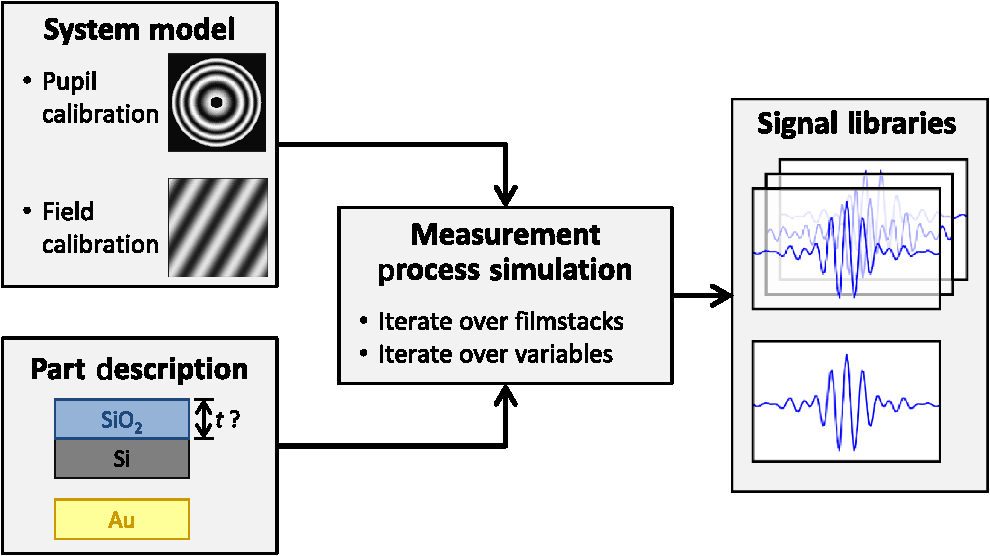
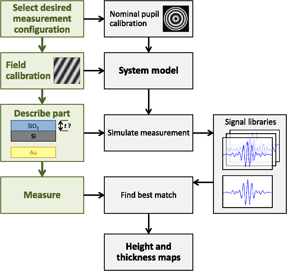
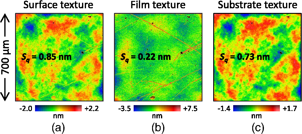
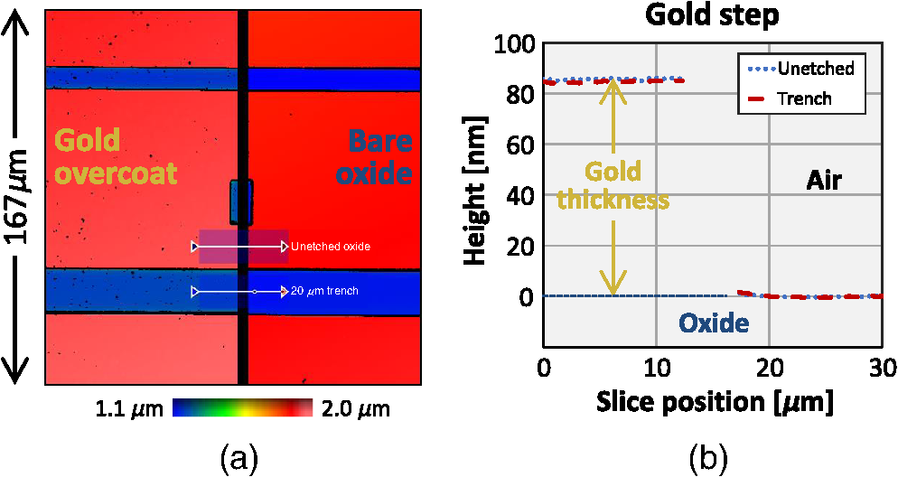
1.Introduction1.1.Surface Metrology with Submicron FilmsSurface metrology must increasingly contend with submicron films, whose prevalence now extends to products well beyond semiconductor devices. These films may be incidental, such as oil on a machined part, or of little direct concern to a user interested only in the top surface. Alternately, the film may be critical, protecting the underlying substrate or providing specific optical characteristics. In any case, adding a submicron film to a component rarely relaxes previous surface metrology requirements. Instead these will generally expand to include film properties, such as thickness, uniformity, and texture. 1.2.Requirements for Surface Films AnalysisIdeally, a surface metrology technology adapted to measure submicron films will retain its performance for topography alone. This includes metrics, such as resolution and throughput, but also extends to configuration flexibility. For microscope-based technologies, this means that films analysis should not restrict the choice of objective or zoom. As for the films metrology itself, associated calibrations should be sample-agnostic—a sample-specific calibration artifact (for example, matching bare substrate) may be costly or impractical. Measurements should exploit the available optical resolution: surface metrology previously producing high-resolution height maps should do likewise for thickness. Finally, surface films analysis should provide unambiguous results over a wide thickness search range. The user may have little knowledge of the thickness or thickness may vary widely over the measurement area. 1.3.Challenge and Opportunity for Coherence-Scanning InterferometryCoherence-scanning interferometry (CSI) provides noncontact areal topography maps with sub-nm precision1,2 over a variety of surface types, including patterned semiconductor wafers, flat panel display components,3,4 automotive machined metal parts,5 transparent film structures, and MEMS devices. CSI determines surface topography from the localized coherence signal produced by interference between reflections from the sample and a reference surface. A typical CSI signal for a bare surface (i.e., no film) is shown in Fig. 1(a): surface location essentially corresponds to the peak envelope position. Fig. 1Typical CSI signals for (a) bare surface (no film); (b) thick film (well over ) with well-separated signals from surface and substrate; and (c) submicron film with merged surface and substrate signals. 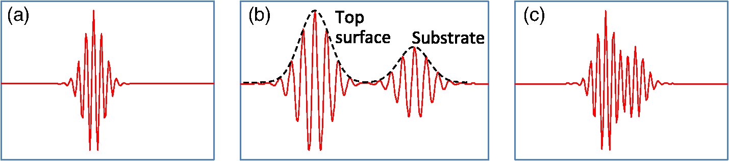 A transparent film will generally produce an additional signal from the substrate. For thick films [Fig. 1(b)], the signals are well separated and can be easily assigned to the top surface and substrate.6,7 However, for sub-micron films the surface and substrate signals merge [Fig. 1(c)] and are no longer separable. But this sensitivity to films also presents an opportunity: if film effects can be modeled, the distorted CSI signal can be decoded to simultaneously determine surface and thickness. 2.Model-Based CSI2.1.OverviewModel-based CSI simulates signals over an expected range of film properties and selects the best match with the measured signal. It has been presented in various forms,8–12 all using frequency-domain analysis to combine models for the system and of the part being measured. Thus a caveat with model-based CSI is that film properties must be at least partly known to bound the search space and avoid degenerate solutions. In practice, this usually requires known visible-spectrum refractive indices for both substrate and film, with film thickness left as the unknown parameter to be determined. The film index is usually assumed to be constant, neglecting for example thickness dependence from quantum size effects13 that can emerge with ultra-thin films. Therefore, model-based CSI is typically most applicable for films that are thicker than about 50 nm. 2.2.Previous ApproachesA CSI signal can be represented as a function of spatial frequency over a range determined by the source wavelengths in conjunction with the incident angles supported by the system [with maximum generally corresponding to the numerical aperture (NA) of the objective]. The wavelength and incident angle can be expressed in terms of angular wavenumber and directional cosine A given spatial frequency will then have contributions from any pairs of and satisfying This suggests modeling the response of the system and the part as a function of and . This is shown in Fig. 2, where a ray bundle for a particular pair passes through a Mirau objective and reflects from the part. As previously presented in detail,9 contributing pairs can be summed incoherently for each spatial frequency , which is discretized using a conventional fast Fourier transform or equivalent. Fig. 2Modeling the response of a CSI system and a measured part to a constituent ray bundle . The depicted configuration of beam-splitter (BS) and reference (Ref.) corresponds to a Mirau objective, but the approach applies equally to other forms of interferometric objectives. 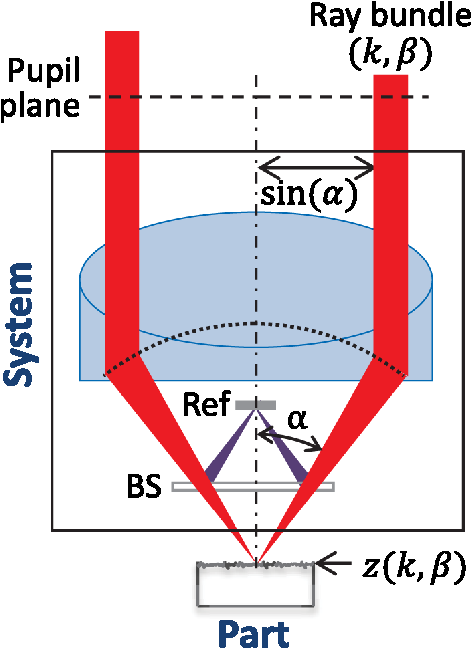 Modeling the complex reflectivity of the part is straightforward14 if refractive indices for the substrate and film are known. For the system, some approaches to model-based CSI approximate incident angle as a single value averaged over the NA.11,15 This simplifies computation to a one-dimensional integration over and allows a straightforward field calibration using a conventional imaging tube-lens in the intended measurement configuration. However, such approaches are limited to lower NA systems. The precursor to the approach presented here supports systems with any NA,16–18 using a system model derived from the objective pupil that captures dependence on both and , as shown in Fig. 2. Signal libraries are then generated over the expected range of film configurations, as shown in Fig. 3. However, performing the requisite pupil calibration requires a specialized Bertrand tube-lens. Also, with earlier approaches, the intensive computation entailed practical throughput trade-offs, typically limiting analysis to small subregions within the field of view. 2.3.Presented ApproachThe approach presented here is similar in principle to its predecessor16 but separates calibration into two parts. Pupil calibration uses a nominal model, thereby avoiding any need for specialized hardware. Field calibration is performed in the desired measurement configuration to capture tool-specific characteristics. The procedure is compatible with any interferometric objective and uses only standard CSI hardware. The full measurement sequence is shown in Fig. 4. The best-match signal search remains nominally unchanged, with the key difference that optimized processing—facilitated by greater computing power—now allows full-field analysis at megapixel camera formats. Processing time depends strongly on the search range and pixel count but is typically under 10 s for full-field analysis of about one million independent pixels. Calibration uses any flat artifact with known visible-spectrum refractive indices. No part-specific calibration is required, which is particularly beneficial for reverse engineering or parts with complex geometries. 3.Example MeasurementsA modern commercial CSI microscope19 was used to measure a variety of parts with submicron films and dissimilar materials. For each measurement configuration, calibration was performed using only a silicon carbide flat, which is also used for standard-CSI calibrations. 3.1.Films Applications Requiring a Wide Search RangeAll model-based approaches have some degree of degeneracy that can produce multiple solutions to the same set of model parameters. For films metrology, the outcome can be ambiguous or incorrect film thickness values that nonetheless yield apparently acceptable matching signals to the experimental data. One solution is to strictly limit the thickness search range; but this may be precluded by incomplete knowledge or by large variations in thickness over the measurement area. A more attractive approach taken here is to identify small but distinctive signal details that allow the removal of potential degenerate solutions and enable a wide search range. Figure 5(a) shows a silicon substrate coated with silicon oxide with center thickness . The outer rim of this coating exhibits a thickness gradient down to zero (bare silicon), where the substrate was masked by the fixture during evaporation. This transition region was measured using a Mirau objective, using an oxide-on-silicon model with a search range of 0 to 1300 nm, and independent processing for all pixels in the field of view. Fig. 5Oxide-gradient sample measured at the film boundary using a Mirau objective: (a) photograph of part showing measurement region; (b) map of oxide thickness ranging from 0 (bare silicon) to ; and (c) profiles of oxide/air and substrate surfaces. 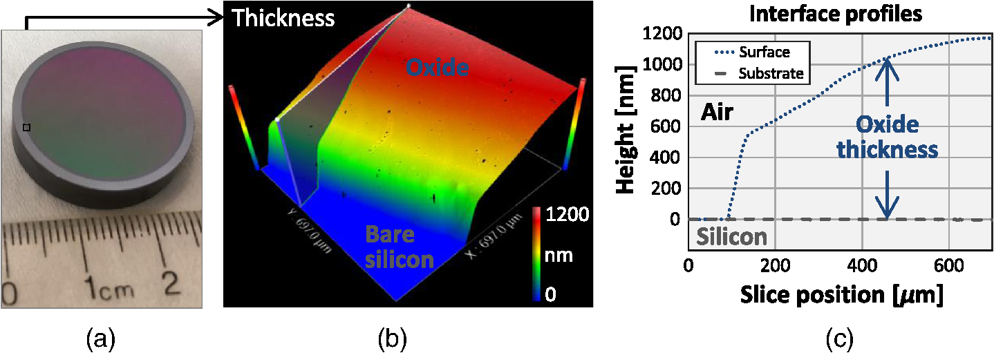 The resulting thickness map and a cross-sectional slice spanning the full thickness range are shown in Figs. 5(b) and 5(c). The thickness variation is continuous and monotonic as expected, indicating that the thickness was determined unambiguously throughout the wide search range. The silicon substrate, derived by subtracting thickness from the top surface, is flat as expected to within . 3.2.Films Metrology over a Wide Range of MagnificationCSI’s large choice of magnifications enables a wide range of surface metrology applications, from measuring form to inspecting microscopic defects. This flexibility remains just as desirable with the addition of thin films, and indeed should extend to the metrology of the film itself. Ideally, model-based CSI should work over the full selection of optical configurations. Figure 6 shows thickness maps measured for an oxide-on-silicon film standard (NIST certified thickness of ) using four different objective/zoom combinations spanning a range in magnification. For all cases, analysis used an oxide-on-silicon model with a search range of 0 to 1200 nm for all pixels in the field of view. The wide search range is deliberate, to verify robustness and emulate the case of film thickness being unknown. Fig. 6Thickness maps for an oxide-on-silicon film standard (certified thickness 96.6 nm), measured over a range of magnification. The agreement in mean thickness is better than 1 nm across all objectives. 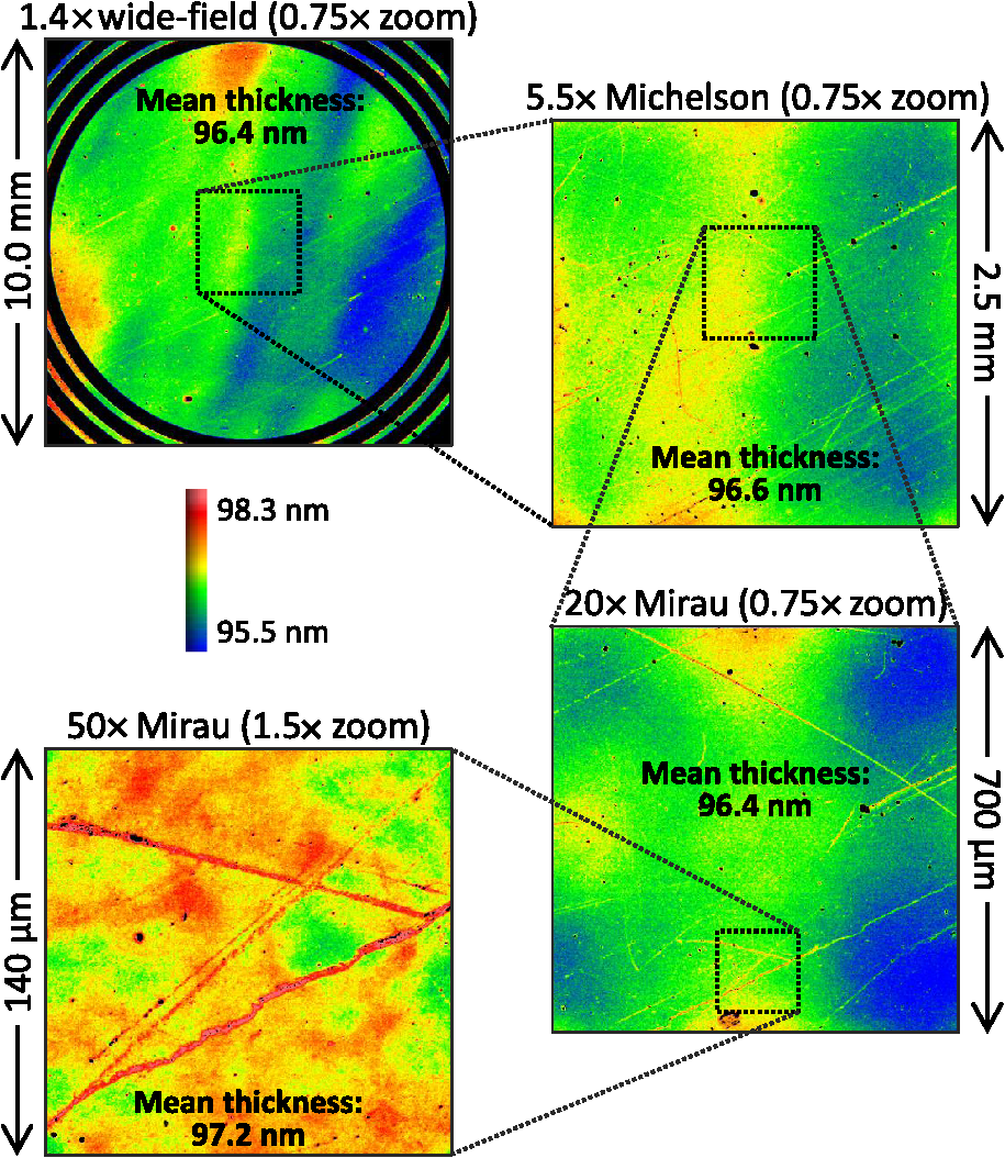 The wide range of magnifications provides a thorough picture of film characteristics. The Zygo wide field (ZWF) objective20 captures the entire certified region in a single field of view, revealing slow variations in film thickness. The concentric rings correspond to deliberate patterning in the film, with black rings indicating where the oxide is etched down to the silicon substrate. Measurements at higher magnifications reveal smaller-scale thickness variations, along with surface scratches resulting from handling of this laboratory sample. The highest-magnification map, obtained with a Mirau, reveals details of individual striation defects. In conjunction with the thickness maps shown in Fig. 6, model-based CSI also provides surface maps. Subtracting film thickness from the top surface yields a derived map of the substrate surface: collectively, these maps enable additional metrology and validation. Again, the range of magnifications enables a thorough surface analysis. Results from the ZWF capture regions of both oxide film and exposed silicon substrate, as shown in Fig. 7. The surface map reveals steps between the oxide and bare silicon. From the manufacturing sequence (blanket thermal oxidation followed by patterned etch down to silicon substrate), we expect that surface steps should match film thickness, or equivalently, that the underlying silicon substrate should be continuous. The substrate map confirms this, validating the overall measurement. Fig. 7Maps for oxide-on-silicon film standard measured using a ZWF objective: (a) top surface, (b) oxide thickness, and (c) silicon substrate.  Measurements at higher magnification reveal textural differences between the surface, thickness, and substrate. Figure 8 shows interface maps obtained from the Mirau, with form (fourth-order polynomial) removed. The top surface exhibits both orange-peel texture and striations. Meanwhile, the film texture is dominated by striations whereas the substrate exhibits orange-peel texture but is free from striations. Collectively these maps reveal that the substrate contributes the orange-peel texture and that the striations reside in the top surface of the film (likely from usage, not an original defect). 3.3.Parts with Dissimilar MaterialsEven bulk materials can confound conventional CSI if there are variations in phase-change on reflection (PCOR), as will occur between dissimilar materials.16 For example, a conventional CSI measurement of a glass/metal step will typically be biased by to 20 nm, with the metal appearing lower than in reality.21,22 More generally, a part can comprise both films and bulk dissimilar materials. Figure 9 shows the fabrication sequence for such a sample, in the form of trenched oxide-on-silicon with a partial gold overcoat. First, of thermal silicon oxide was grown on a silicon substrate. Next trenches were formed in the oxide via photoresist masking and a partial etch, deliberately leaving thinner oxide at the trench bottom. Finally, trenches were partially gold-coated by a lift-off sequence (photoresist masking, global gold deposition, and photoresist strip). Target gold thickness was , sufficient to essentially eliminate film effects from the underlying oxide. Fig. 9Fabrication sequence for oxide trench sample with partial gold overcoat: (a) grow of thermal oxide on a silicon substrate; (b) form oxide trench; and (c) deposit partial gold overcoat. 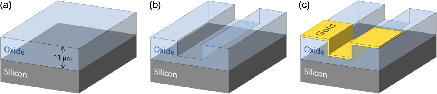 This sample was measured using a Mirau objective, with analysis tailored to each region: for the uncoated oxide, an oxide-on-silicon model with a search range of 0 to 1200 nm; and for the gold overcoat, a bulk-gold model (i.e., no film). Figure 10 shows surface and thickness maps for a pair of trenches over a gold-coating boundary. Fig. 10Maps for (a) surface and (b) bare-oxide thickness of trench-oxide sample, measured using a Mirau objective. 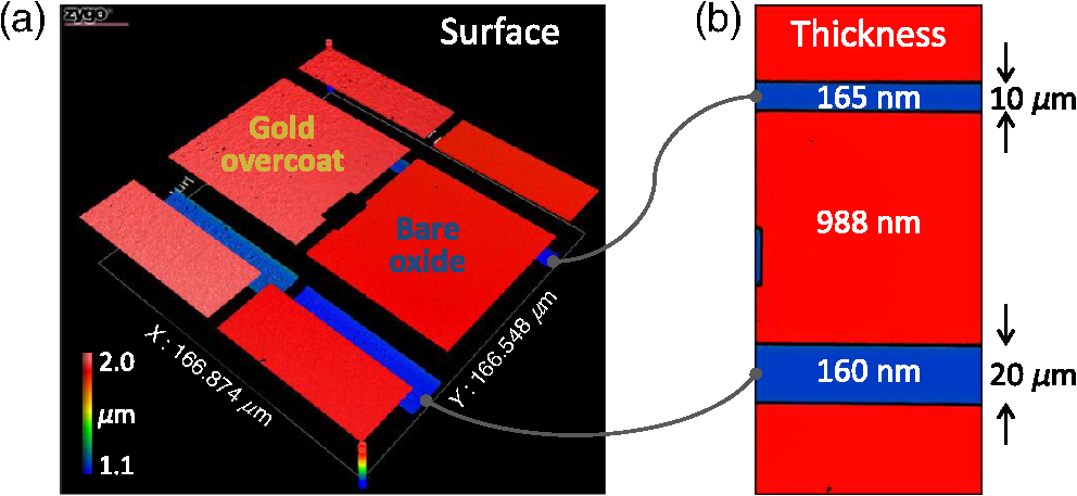 The thickness of the unetched oxide was measured to be 988 nm. For the trenches, thickness depends slightly on their width: 160 nm for the trench and 165 nm for the trench. By subtraction, thickness results suggest trench depths of 828 and 823 nm for the 20- and trenches, respectively. This is corroborated by the results of Fig. 11, which shows cross-sectional surface-map profiles through both trenches, and on both sides of the coating boundary, i.e., with and without gold overcoat. The trench is shallower than the wider trench, and is consistent with its oxide thickness measuring as 5 nm thicker, as in Fig. 10(b). Moreover, measured trench depths agree with thickness-suggested results to better than 1 nm. Overall, surface and thickness results reveal that the oxide-etch process was about 0.6% slower in the narrower trench. As further corroboration, trench-depth measurements on either side of the coating boundary—obtained using completely independent analyses, with and without film effects—agree to better than 1 nm. This self-consistency extends earlier work16,18 demonstrating nm-level agreement between trench depths measured with model-based CSI and an atomic force microscope. Fig. 11Surface profiles for trenches with width 10 and : (a) surface map showing locations of profiles on each side of gold-coating boundary and (b) plots of profiles. 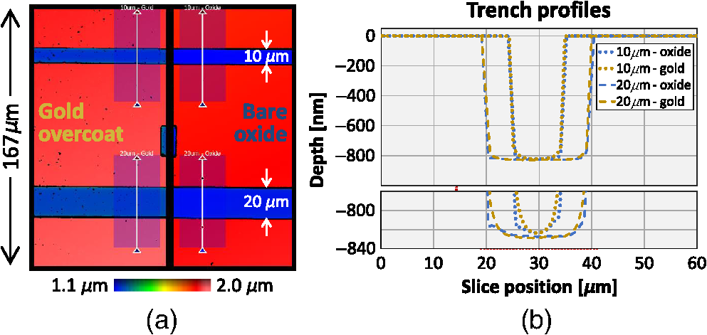 Some applications require correct topography across dissimilar regions. For this sample, this corresponds to the gold-thickness step across the coating boundary. Figure 12 shows gold-thickness profiles measured over dissimilar oxide film thicknesses: 160 nm within the trench and 988 nm in adjacent unetched oxide. Both profiles indicate a gold thickness of about 85 nm with agreement to . 4.SummaryThe presented approach to model-based CSI enables full-field films surface metrology over a full range of interferometric objective magnification, producing high-resolution maps of surface and film thickness. Calibration is sample-agnostic, and for most practical search ranges, measurement time is comparable to that of conventional CSI. Beyond transparent films, model-based CSI provides PCOR-corrected topography for any combination of dissimilar materials with known visible-spectrum refractive indices, including metals. Results demonstrate single-nm self-consistency between topography and thickness maps, provided refractive indices are well known. This represents an important caveat with model-based CSI: poor knowledge of material properties will limit performance and may even prevent a meaningful measurement. A natural next step for model-based CSI would be to extend capabilities to tolerate uncertainty in material properties. AcknowledgmentsThe original work presented in this paper benefited from key contributions and input from Xavier Colonna de Lega, Jim Kramer, and Peter de Groot. ReferencesP. de Groot,
“Principles of interference microscopy for the measurement of surface topography,”
Adv. Opt. Photonics, 7
(1), 1
–65
(2015). http://dx.doi.org/10.1364/AOP.7.000001 Google Scholar
Geneva
(2013). Google Scholar
D. Grigg et al.,
“New optical metrology techniques for color filter inspection and process control,”
in Proc. IDW 11th Int. Display Workshops,
(2004). Google Scholar
Z. He et al.,
“New optical 3D-CD metrology techniques for liquid crystal display manufacture inspection and process control,”
in Proc. Asia Display,
(2007). Google Scholar
J. C. Wyant,
“How to extend interferometry for rough-surface tests,”
Laser Focus World, 29 131
–135
(1993). LFWOE8 1043-8092 Google Scholar
P. A. Flournoy, R. W. McClure and G. Wyntjes,
“White-light interferometric thickness gauge,”
Appl. Opt., 11 1907
(1972). http://dx.doi.org/10.1364/AO.11.001907 APOPAI 0003-6935 Google Scholar
X. C. de Lega and P. de Groot,
“Transparent film profiling and analysis by interference microscopy,”
Proc. SPIE, 7064 70640I
(2008). http://dx.doi.org/10.1117/12.794936 PSISDG 0277-786X Google Scholar
P. de Groot and X. C. de Lega,
“Signal modeling for low-coherence height-scanning interference microscopy,”
Appl. Opt., 43 4821
–4830
(2004). http://dx.doi.org/10.1364/AO.43.004821 APOPAI 0003-6935 Google Scholar
S.-W. Kim and G.-H. Kim,
“Thickness-profile measurement of transparent thin-film layers by white-light scanning interferometry,”
Appl. Opt., 38 5968
(1999). http://dx.doi.org/10.1364/AO.38.005968 APOPAI 0003-6935 Google Scholar
D. Mansfield,
“The distorted helix: thin film extraction from scanning white light interferometry,”
Proc. SPIE, 6186 61860O
(2006). http://dx.doi.org/10.1117/12.664036 PSISDG 0277-786X Google Scholar
N. A. Mancini, G. Giaquinta and A. Pennisi,
“Quantum size effects and optical properties of very thin films,”
J. Opt. Soc. Am., 71 383
–385
(1981). http://dx.doi.org/10.1364/JOSA.71.000383 JOSAAH 0030-3941 Google Scholar
M. Born and E. Wolf, Principles of Optics, 62 6th Ed.Pergamon, Oxford
(1987). Google Scholar
H. Yoshino et al.,
“Measurement of thin film interfacial surface roughness by coherence scanning interferometry,”
J. Appl. Phys., 121 105303
(2017). http://dx.doi.org/10.1063/1.4978066 JAPIAU 0021-8979 Google Scholar
P. de Groot and X. C. de Lega,
“Optical topography measurement of patterned wafers,”
in AIP ULSI Conf. Proc.,
432
–436
(2005). http://dx.doi.org/10.1063/1.2062999 Google Scholar
X. C. de Lega and P. de Groot,
“Characterization of materials and film stacks for accurate surface topography measurement using a white-light optical profiler,”
Proc. SPIE, 6995 69950P
(2008). http://dx.doi.org/10.1117/12.782836 PSISDG 0277-786X Google Scholar
(2013). Google Scholar
P. de Groot and J. F. Biegen,
“A new class of wide-field objectives for 3D interference microscopy,”
Proc. SPIE, 9525 95250N
(2015). http://dx.doi.org/10.1117/12.2183628 PSISDG 0277-786X Google Scholar
J. F. Biegen,
“Determination of the phase change on reflection from two-beam interference,”
Opt. Lett., 19 1690
–1692
(1994). http://dx.doi.org/10.1364/OL.19.001690 OPLEDP 0146-9592 Google Scholar
M.-C. Park and S.-W. Kim,
“Compensation of phase change on reflection in white-light interferometry for step height measurement,”
Opt. Lett., 26 420
–422
(2001). http://dx.doi.org/10.1364/OL.26.000420 OPLEDP 0146-9592 Google Scholar
BiographyMartin F. Fay is a senior research scientist at Zygo Corporation, specializing in advanced solutions for optical dimensional metrology and surface analysis. He holds a PhD in electrical engineering from Brown University and a MASc degree from the University of Toronto for inventive contributions to binary supergratings and multiwavelength lasers. His current research interests include interferometry, films metrology, and algorithms. Thomas Dresel is a senior research scientist at Zygo Corporation. He received both his diploma degree and a PhD in physics from the University of Erlangen in 1991 and 1996, respectively, for contributions on short coherence interferometry and diffractive optics. He joined Zygo in 2002 and since then has been involved in the development of ultrahigh precision instruments for the measurement of aspheres, free-forms, and film structures. His research interests include interferometry, algorithms, and visualization techniques. |