|
|
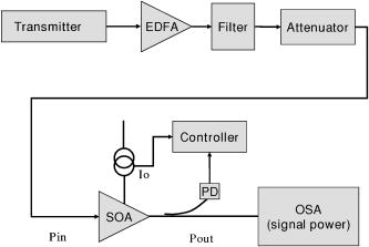
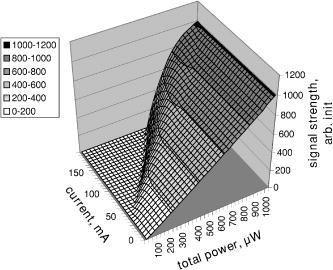
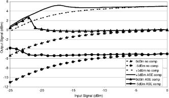
1.IntroductionSemiconductor-optical amplifiers (SOAs) are key future components in the evolution of all-optical networking. They are flexible not only in terms of functionality, e.g., amplification, gating, and switching,1, 2, 3 but can be designed to operate over a wide wavelength range from 0.6 to . More recently, the sharp increase in demand for high-speed access solutions for both business and home usage has stimulated opportunities within passive optical networks (PONs) deployment strategies.4, 5, 6, 7 In addition to traditional telecoms applications, SOAs are also being used as the active element in sensor and measurement systems,8 some of which operate at . For many applications, it is advantageous to regulate the SOA gain such that the signal power remains constant at the output. This can readily be implemented through the use of a monitor photodiode and a tap coupler positioned at the amplifier output. However, particularly in the case of high gain SOAs, the amplified spontaneous emission (ASE) strength at the output of the SOA can be comparable with the signal strength, and consequently can compromise the control of the signal strength. This work reports on the design of an automatic power control system that compensates for ASE through knowledge of the SOA drive current. 2.Background and ConceptAutomatic power control (APC) can be implemented by measuring a small portion of the amplifier output with a photodiode and using negative feedback to hold the photodiode signal constant (see Fig. 1). However, in addition to the signal of interest, the amplifier emits amplified spontaneous emission noise (ASE). The monitor diode responds to this noise and consequently, the APC controls the sum of signal and noise powers. As a result, control of the signal power is compromised, particularly at low input signal strengths where significant gain is required. To address this issue, an optical filter may be placed in line with the monitor photodiode to reject the ASE, allowing the APC to operate only in response to changes in the signal strength. However, this increases the cost and fixes the amplifier use to one particular wavelength division multiplex (WDM) channel. A tap and monitor photodiode at the amplifier input can give insight to the incoming signal strength and thus offer a means with which to correct for errors associated with the ASE strength. Again, this represents additional cost, and furthermore the SOA noise figure is increased by an amount corresponding to the tap coupler insertion loss. This work reports on a means of addressing these limitations using a direct measurement of the SOA drive current in combination with the total output power to estimate the output signal strength. This does not incur additional cost, since the drive current measurement is already implemented as part of the current regulation. 3.MethodologyThe process relies on establishing a relationship between the total output power (signal and ASE) from the SOA and the output signal strength. This is not trivial, since the ASE level is a function of amplifier gain (G), and the amplifier gain depends on population inversion (drive current) and also the input signal strength. The relationship between gain and signal strength is approximated by9 where is the maximum saturated output power of the amplifier, and is the maximum gain. Consequently, as the signal strength increases, the gain saturates and the ASE level falls. However, since the small signal gain, , the , and maximum gain value are themselves functions of the amplifier inversion factor, and consequently related to the drive current, it is not possible to establish a direct analytical relationship between total output power and output signal strength for a given input signal. As a result of this, APC schemes based on processing the total output power to recover signal and ASE levels independently have, to our knowledge, not previously been implemented. This work therefore presents novel data describing a practical solution based on determining this relationship experimentally. The process enables an error signal, which can be used to facilitate the APC process, to be obtained as follows.The SOA was driven through all possible combinations of input signal strength (in this case, limited to ) and drive current and the output signal strength and the total power output recorded for each of these points. These data were used to calculate a 3-D map relating the “desired” signal strength to any given combination of total output power and amplifier drive current. This map was loaded into the microcontroller chip controlling the SOA drive current. The APC process uses the monitor diode power and drive current as pointers to the map to find the corresponding signal strength, and adjusts the drive current based on how that signal strength compares to the user’s setpoint. As a result, the APC responds to the signal alone, as if there were a filter in the power monitor tap. In principle, since there is no optical filter, the process wavelength is transparent. In practice, significant gain variation across the signal band of interest (gain variation can be around across the c-band for a high gain SOA1) will cause the amplifier to saturate at different input signal strengths for different wavelengths, and will restrict the range of operation before recalibration is necessary. Interpolation may be used to minimize the characterization required; however, this has not been addressed to date. Once the amplifier is characterized, the process requires only a microcontroller chip of reasonable power and memory capacity to implement the control algorithm. Generally, this could be accommodated with the chip used to perform the SOA current stabilization and temperature control. This work reports on a demonstration of this concept using a low-power-reduced instruction set (RISC) processor, the microchip PIC16E877.10 3.1.Making the MapThe APC process hinges on the assumption that control of the SOA can be approximated to a two degree of freedom system, requiring only knowledge of two independent variables, describing its state to calculate any of the others. This assumption is reasonable, given that the SOA only has three inputs: optical signal, drive current, and temperature control. If the temperature is kept the same at all times, as it generally is, then there are only two inputs. Everything that occurs within the SOA must therefore be a function of those two inputs, optical signal and drive current. The argument ignores long-term aging effects, but it is assumed that this can be addressed through appropriate modeling. The argument also relies on the assumption that the input optical signal to noise (OSNR) is sufficiently high to permit the input ASE contribution to be neglected. With postfiltering of the input signal (e.g., after demultiplexing), this assumption is also reasonable. Finally, gain variation and polarization dispersion (PDG) are deemed to be insufficient, over the wavelength band of interest, to make the output signal a three (or four) variable system—amplitude, wavelength, signal-to-noise ratio (SNR), and polarization state. Since most applications specify PDG to be less than , polarization variation can generally be neglected. Gain variation over the wavelength range of interest can be significant, but this can be accommodated for by characterizing the amplifier over the wavelength range of interest. The APC algorithm will need knowledge of the operating wavelength, but no additional physical components are required. The following details an experimental evaluation of this concept. 4.ExperimentA test rig was established comprising a signal source, an SOA with monitor diode, and an optical spectrum analyzer (see Fig. 1). The signal source comprised a tunable laser, an erbium-doped fiber amplifier (EDFA); a tunable filter to remove ASE from the EDFA, and a variable attenuator. The signal was fed into an SOA controlled using a driver with an onboard monitor diode. The output of the SOA was recorded using the monitor photodiode as a function of input signal strength ( to ) and drive current. For each point, the “desired” or “target” signal strength was recorded using an optical spectrum analyzer (OSA). Thus a map that relates the target output signal strength to a measurement of the total output power at each bias current point was generated. An example of this is shown in Fig. 2. To implement that APC, the desired signal strength is input to the controller. This, through the map obtained before, defines the controller set point for any given drive current. The controller then derives an error signal from measurement of the total optical output power and the set point value, and adjusts the bias current until the set point and monitor power values agree. At this point, the signal power will be at the desired value. 4.1.ImplementationThe map generated before is then edited into a 10-bit representation suitable for implementing the controller. Figure 2 is a 3-D representation of the finished map as loaded into the processor memory. Note the desired signal strength and total output power are represented by a 10-bit digit. This can be readily scaled to represent real values. 4.2.Map Size, Resolution, and FilteringThe size of the map is a tradeoff between memory capacity and processing speed. Our prototype system, for example, used a 20-MHz microcontroller with of memory. The memory limitation led us to reduce the map size to locations, taking up of memory. This gave a resolution of only one part in 32 , which is lower than desirable (one part in 1024- ). The limitations of the processor used rendered a map impractical. To address this limitation, the APC controller was implemented using a bilinear filtering algorithm to interpolate values from their four nearest neighbors. The bilinear filter was written in assembly language, optimized for speed, and interpolated the five least-significant bits, giving 10-bit resolution at a speed of about 100 samples per second. The sampling rate directly limits the time constant of the APC control loop, so that our prototype had a response time of about . 5.Results and DiscussionResults of early stage trials of the APC system are displayed in Fig. 3. The graph shows the difference between APC implemented without processing the output signal to compensate for ASE, and the case where ASE is accounted for through the procedure described before. Here, the effectiveness of the ASE-compensated APC is clearly visible. In all cases, a significant drop off from the target output signal strength is observed without ASE compensation, particularly at low input signal strength, where the ASE contribution becomes more significant. In the case where the target signal power is , the actual signal strength is low when the input power falls below and is low at input power. In contrast, the ASE corrected signals are accurate to approximately over an input power range, which extends to . The APC does become nonlinear at lower input powers, but for most applications these would not be relevant. 6.SummaryThe output from an optical amplifier is a combination of the signal strength and the spontaneous emission. We present an automatic power control system that derives a representation of the output signal strength from a measurement of the total output power and the amplifier drive current. This enables an error signal to be derived that compensates for the influence of ASE and eliminates the need for wavelength selective filters and/or power monitors at the input of the amplifier, thus offering a route to lower implementation costs. APC, which is accurate to , is demonstrated over a range of input powers down to . Significant gain variation over the wavelength range of operation may introduce an offset error. This has as yet not been quantified experimentally. However, the controller can in principle compensate for this variation, provided the wavelength response of the amplifier is known and the operating wavelength is specified. We demonstrate APC with a precision of with input signals ranging down to using a low power microprocessor to implement the processing real time. ReferencesK. Morito,
M. Ekawa,
T. Watanabe, and
Y. Kotaki,
“High-output-power polarization-insensitive semiconductor optical amplifier,”
J. Lightwave Technol., 21
(1), 176
–181
(2003). https://doi.org/10.1109/JLT.2003.808643 0733-8724 Google Scholar
K. Wakao,
H. Soda, and
Y. Kotaki,
“Semiconductor optical active devices for photonic networks,”
Fujitsu Sci. Tech. J., 35 100
–106
(1999). 0016-2523 Google Scholar
T. Ito,
N. Yoshimoto,
K. Magari, and
H. Sugiura,
“Wide-band polarization-independent tensile strained MQW-SOA gate,”
Photon. Technol. Lett., 10
(5), 657
–659
(1998). Google Scholar
D. B. Payne and
J. R. Stern,
“Wavelength switched, passively coupled, single mode optical networks,”
(1985). Google Scholar
N. SuzkukiNakagawa,
“First demonstration of full burst optical amplified GE-PON uplink with extended system budget of up to 128 ONU splits and reach,”
141
–142
(2005). Google Scholar
P. Healey,
P. Townsend,
C. Ford,
L. Johnston,
P. Townley,
I. Lealman,
L. Rivers,
S. Perrin, and
R. Moore,
“Reflective SOAs for spectrally sliced WDM-PONs,”
352
–353
(2002). Google Scholar
P. P. Iannone,
K. C. Reichmann, and
L. H. Spiekman,
“Amplified CDWM systems,”
678
–679
(2003). Google Scholar
G. D. Lloyd,
L. A. Everall,
K. Sugden, and
I. Bennion,
“Resonant cavity time-division-multiplexed fiber Bragg grating sensor interrogator,”
Photon. Technol. Lett., 16
(10), 2323
–2325
(2004). Google Scholar
R Ramaswami, Optical Networks, 210 Academic Press, San Diego, CA (1998). Google Scholar
|