|
|
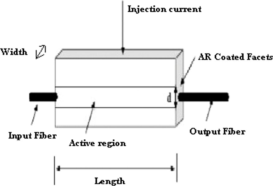
1.IntroductionWith the tremendous growth of computing technology, the need of high-performance computers has significantly increased. Optics has been used in computing for a number of years. Optical computing was a hot research area in 1980’s, but the work tapered off due to material limitations that prevented opto chips from getting small enough and cheap enough beyond laboratory curiosities. Now, developments in the field of optical computers are back with the development of nonlinear organic material and semiconductor technology.1 The semiconductor optical amplifier (SOA) is one of the most frequently used devices for ultrafast all-optical computing. In the SOA, population inversion is realized by current injection. When we put in an intense gate pulse, it causes gain reduction and an associated refractive index change takes place. This is the third-order nonlinear effect. A characteristic feature of this response is that it is very fast for the rise time; however, there is a slow component on the order of 1 ns in the response recovery, which is the band-to-band recombination lifetime. This slow component has been the obstacle in realizing ultrafast switching devices above .2 Two methods are described for solving this problem. One is to use a wavelength filter to select only the very fast component of the response. Another method is to use the SOA in a Mach–Zehnder interferometer configuration. This paper discusses the properties of SOAs and how these properties can be utilized to develop all-optical computing devices. In Sec. 2, a brief review of the basic properties of SOAs and its features as an ultrafast nonlinear device have been discussed. Section 3 introduces two ways of using SOAs for ultrafast signal processing: one is to use only the very fast response component of SOAs with wavelength filter and the other is to cancel out the slow response component of SOAs using the Mach–Zehnder interferometer configuration. We review the progresses in SOA-based all-optical computing devices using the above two concepts. Out of the research papers based on similar methods, few have been included in the list of references as there is a lot of research work going on in these techniques. Section 4 describes the simulation results for the gain saturation characteristic of SOAs, which is the main characteristic for using SOAs in optical computing devices. 2.SOAs as an Ultrafast Nonlinear DeviceThe basic structure of a SOA is given in Fig. 1. An intrinsic layer called the active layer is sandwiched between -type material and -type material layers. By selecting a different material composition for the active layer, it is possible to create a lower band gap with respect to its surrounding layers. When a forward voltage is applied over this heterostructure, free electrons from the -type material and holes from the -type material will travel towards the active layer. Here the electrical carriers will accumulate as they are trapped in this low band gap potential well. By applying appropriate pumping, large concentrations of electrons and holes build up in the active layer, which leads to population inversion. Photons from incoming light passing through the amplifier medium can trigger electrons in the conduction band to relax to their ground state and recombine with holes in the valence band. As a result, photons with the same wavelength and phase as the incoming photons will be emitted and stimulated emission (SE) occurs. On the other hand, an electron that still is in its ground state can again absorb the energy of a passing photon and gets excited. This process is in fact the opposite of SE and is known as stimulated absorption (SA). When population inversion is sufficiently large, the SE will dominate the SA and light amplification is achieved. So the light amplification process in an SOA can be described, by applying a large enough injection current population inversion is achieved. When light is coupled into the amplifier, SE occurs resulting in amplification of the incoming light. The optical gain of the SOA with a bulk or quantum well active layer can be obtained as:2 where is the optical confinement factor that accounts for the guiding of radiated photons by the waveguide structure of an active region, is the gain coefficient of an active region per unit of length, and is the loss coefficient of a cavity per unit of length. In addition to this, the gain coefficient () depends on the frequency () and power of the signal being amplified () so that . Concentrating on power, the gain coefficient is given by:2The quantum dot active layer exhibits a discrete gain peak due to its three-dimensional quantization. The output power saturation takes place because of the reduced population inversion caused by the intense optical power that consumes the population inversion carriers. As for polarization dependence, a waveguide with a thin active layer gives a small loss to the TE mode when compared with that for the TM mode, resulting in polarization dependence. There are various designs of the active layer for minimizing polarization dependence. If we want to have large saturation power and polarization insensitive response, the bulk active layer SOA may be the most convenient available device. Table 1 below summarizes the characteristics of various SOAs.2 Table 1Characteristics of various SOAs.
When we consider the use of the SOA for ultrafast signal processing, the most inconvenient feature is the slow response associated with carrier recombination. As mentioned above, there are two methods to overcome this slow response. One is the direct use of the ultrafast response by selecting only the fast response using a wavelength filter. The other is the use of SOAs in a Mach–Zehnder interferometer configuration with SOAs at each arm to cancel out the slow response component. In both these configurations nonlinear optical effects associated with the carrier density change in SOAs are utilized. The following are the main nonlinear effects associated with SOAs:
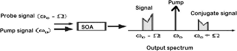
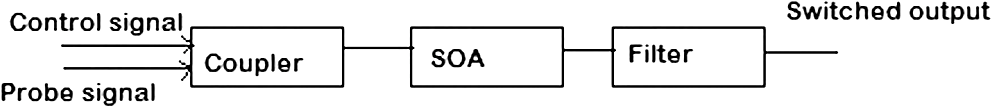
2.1.Cross Gain ModulationThe material gain spectrum of SOAs is homogenously broadened, i.e., a change in the carrier density inside the amplifier will affect the input signals, so it is possible for a strong signal at one wavelength to affect the gain of a weak signal at another wavelength. This nonlinear mechanism is called XGM. The basic XGM is shown in Fig. 2, where a weak continuous wave (CW) probe light and a strong pump light, with a small-signal harmonic modulation at angular frequency , are injected into the SOA. XGM in the amplifier will impose the pump modulation on the probe. This means that the amplifier is acting as a wavelength converter.3 The information in the pump signal will be transferred to the probe signal, i.e., the carrier signal and hence it will work as wavelength converter. The most useful figure of merit of this converter is the conversion efficiency, defined as the ratio between the power of the output probe to the power of the input pump. The wavelength conversion techniques-based SOAs are attractive because of their high-gain, high-saturation output power, wide-gain bandwidth, compactness, and integratibility with other photonic devices. The XGM, one of several wavelength conversion techniques based on SOAs, is simple to implement and has shown impressive operation for a high bit rate. Moreover, the output of optical computing devices using XGM in SOA shows insensitivity to the polarization of input signals. 2.2.Self Phase ModulationThe physical mechanism behind SPM is gain saturation, which leads to intensity-dependent changes of the refractive index in response to variations in carrier density. Signal-gain saturation in SOAs is caused by a reduction of the population inversion in the active layer due to an increase in SE. Gain saturation characteristics are especially important in optical repeaters and multi-channel amplifiers which require high-power operation. Single channel nonlinear effects manifest mainly through SPM, i.e., each channel alters its own phase and with more than one wavelength, the phase of each signal is modified by the power of neighboring channel. This nonlinearity produces a carrier induced phase modulation of the propagating signal, which is called the Kerr optical effect. SPM is desirable to have all-optical components for buffering and delaying signal pulses. Tuneable all-optical delays are important for application in telecommunication, optical coherence tomography, and optical sampling. 2.3.Cross Phase ModulationThe refractive index of an SOA active region is not constant but is dependent on the carrier density and so the material gain. This implies that the phase and gain of an optical wave propagating through the amplifier are coupled via gain saturation. If more than one signal is injected into an SOA, there will be XPM between the signals. XPM can be used to create wavelength converters and other functional devices. However, because XPM only causes phase changes, the SOA must be placed in an interferometric configuration to convert phase changes in the signals to intensity changes using constructive or destructive interference. For two interacting wavelengths the XPM-induced frequency shift depends on wavelength, effective area, and variation in pulse power with time. To take advantage of XPM-induced phase shifts for ultra-fast optical switching, many interferometric methods have been used. Consider an interferometer designed in such a way that a weak signal pulse, divided equally between its two arms, experiences identical phase shifts in each arm and is transmitted through constructive interference. When a pump pulse at a different wavelength is injected into one of the arms, it will change the signal phase through XPM phenomenon in that arm. If the XPM-induced phase shift is large (close to ), this phase shift results in destructive interference and hence no transmission of signal pulse. Thus, an intense pump pulse can switch the signal pulse. 2.4.Four-Wave MixingFWM is a coherent nonlinear process that can occur in SOAs between two optical fields, a strong pump at angular frequency and a weaker signal (or probe) at , having the same polarization. The injected fields cause the amplifier gain to be modulated at the beat frequency . This gain modulation gives rise to a new field at , as shown in Fig. 3. FWM generated in SOAs can be used in many applications, including wavelength converters, dispersion compensators, optical demultiplexers, and optical switching devices. 3.Application of SOAs as Ultrafast Computing DevicesThe main obstacle in the application of SOAs in optical computing devices is its slow recovery time. This problem can be overcome by either using 1) SOAs with a wavelength filter for ultrafast computing or using 2) SOAs in the Mach–Zehnder interferometer configuration. 3.1.SOAs with Wavelength Filters for Ultrafast ComputingOptical filtering of output light to select only the ultrafast component is a powerful technique and has been utilized frequently to enhance the modulation bandwidth of SOA-based optical switches. This method has been successfully used for all optical wavelength conversions at 10,4 40,5 80,6,7 160,8 and ,9 and optical demultiplexing from 320 to .10 Figure 4 depicts a basic block diagram of an all-optical switch based on an SOA followed by an optical band pass filter (BPF). Injected data pulses alter the gain and refractive index of the SOA resulting in amplitude modulation and chirp of the co-propagating CW probe light. The leading and trailing edges of the amplitude-modulated probe light are red and blue shifted, respectively. The data pulses are rejected by the BPF, while a part of the probe light is transmitted. When the BPF is detuned towards the shorter wavelength (blue shift) with respect to the probe light, the amplitude-modulated signal recovers much faster than in the absence of the BPF.8 In the diagram of the all-optical switch mentioned in Fig. 4, short optical pulses are injected into the SOA as a control signal along with a strong CW probe light. Table 2 summarizes the results of experiments/simulations that employed SOA-based optical switches assisted by optical filtering.4–10 Wavelength conversion has been demonstrated for bit rates up to . Since the polarity of wavelength-converted return-to-zero (RZ) signal is inverted by XGM, notch filters that suppress the DC component were used after BPFs to obtain non-inverted data signals. Notch filters were realized using polarization interferometers. Using a similar principle, all-optical demultiplexing was demonstrated in which 160- and optical time-division-multiplexed data streams were demultiplexed into base-rate channels. In this experiment, a CW probe light used in wavelength conversion was replaced with a 40-GHz clock signal.8 One of the advantages of SOA optical switches with optical BPFs is their simple configuration enabling photonic integration. Table 2Optical signal processing using SOA-based optical switches assisted by optical filtering.
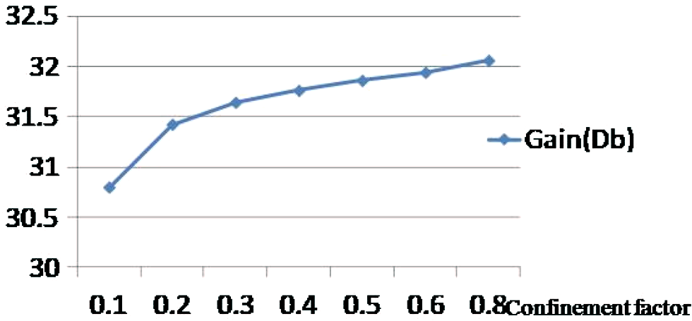
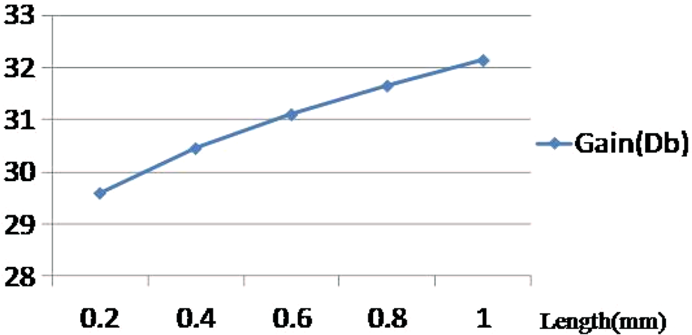
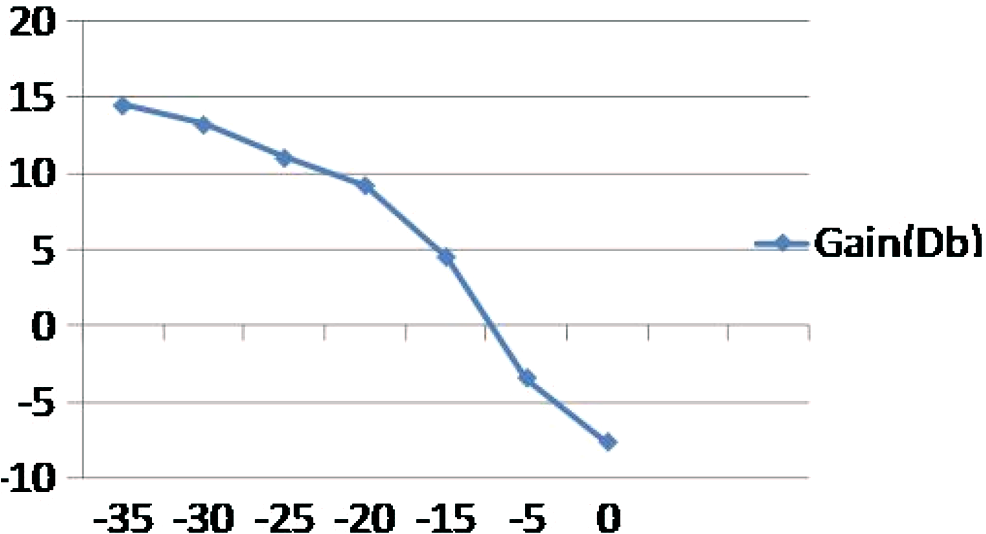
In addition to the above, many optical computing devices using SOAs followed by optical BPF have been reported in recent years, like reconfigurable photonic logic gates based on various nonlinearities in single SOAs has been reported,11,12 all-optical flip-flop using SOAs with DFB laser diode optical feedback combination has been proposed,13 all optical half adder design using equations governing XGM and FWM effect in SOAs have been reported,14 and NAND gate, flip-flop, and finally three input serial shift register have been demonstrated.15 3.2.SOAs in the Mach–Zehnder Interferometer ConfigurationIn all-optical signal processing using SOAs in the Mach–Zehnder interferometer configuration, nonlinear optical effects associated with the carrier density change in SOAs are utilized. The slow response component due to the band-to-band electron recombination is cancelled out using a differential phase modulation scheme. Figure 5 shows the configuration of Mach–Zehnder interferometer wavelength converter in asymmetric and symmetric form.16 SOAs used as nonlinear waveguides are placed in both arms of a Mach–Zehnder interferometer. The control light governs the dynamics of nonlinear optical effects and the probe light experiences the nonlinear optical effects. The control light can be either RZ pulses or non-return-to-zero (NRZ) light. In SOAs, the control pulse induces carrier depletion and thus, modulates the gain and phase of the probe light. These phenomena are called XGM and XPM, respectively. XPM is further converted into intensity form by using differential phase modulation scheme. Fig. 5Configuration of a Mach–Zehnder interferometer wavelength converter in asymmetric and symmetric form. 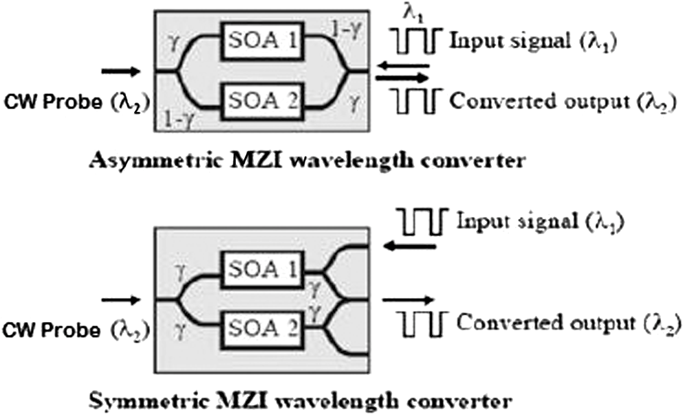 These nonlinear optical effects induced through the carrier density change in semiconductors, are highly efficient, which means that device operation can be realized in a compact size and with low power control light. In addition to this, the control light, which depletes carriers, is amplified in SOAs. This further lowers the required power of input control light. The major obstacle in using XGM and XPM with the carrier density change in SOAs is its slow relaxation time. Typical relaxation times are in the range of 100 ps to 10 ns. In all-optical gates using the SOA-MZI configuration, however, by exciting the two SOAs arranged on both arms of the Mach–Zehnder interferometer with an appropriate time delay, the effect of the slow relaxation is cancelled out. The dynamics of the carrier density in SOAs and associated nonlinear optical effects can be analyzed by rate equations:2 and where is the carrier density, is the rate of carrier injection through bias current, is the transparency carrier density, is the control light power, is the probe light power, is the control light frequency, is the probe light frequency, is the differential gain, is the carrier lifetime, is the light confinement factor, and is the optical loss coefficient including absorption and scattering. The phase shift is proportional to the total carrier number in the SOA (the integral of along the entire length of the SOA). This is a good approximation for the estimation of phase shift. In fact, there are various configurations that utilize the mechanism of cancelling out the relaxation tail of carrier density change. One of the important points for categorizing these configurations is whether the control light and the probe light are co-propagated or counter-propagated through the SOAs used as nonlinear waveguides. When the probe light is counter-propagated with the control light, the gate window shape is influenced by the time during which the control light propagates through the entire length of the SOA.Some important works on optical computing devices based on SOA-MZI are: all-optical flip-flop using two coupled MZIs with an SOA in one arm of each MZI,17 all-optical flip-flop using a bistable laser diode with MZI,18 all-optical error detection circuit using SOA-MZI based XOR gate,19 quantum dot SOA-MZI based high-speed gates,20 and data format conversions based on SOA-MZI have been reported.21 In a general analysis of SOAs, the influence of the amplified spontaneous emission (ASE) is also important. However, in the situations considered here for all-optical signal processing, control light highly depletes carriers in SOAs and so, neglecting the effect of ASE, still gives a good approximation to the carrier dynamics of SOAs. 4.Simulation ResultsAmplification of ultra-short optical pulses in SOA produces considerable spectral broadening and distortion due to the nonlinear phenomenon of self-phase modulation. The physical mechanism behind SPM is gain saturation, which leads to intensity-dependent changes of the refractive index in response to variations in the carrier density. Signal-gain saturation in SOA is caused by a reduction of the population inversion in the active layer due to an increase in SE. The experimental set up used for studying the SOA gain saturation characteristic is shown in Fig. 6. This section describes the effect of the optical confinement factor and length of the active region of the SOA on the gain of the SOA as shown in Figs. 7 and 8. Variation in gain with input power has also been analyzed as shown in Fig. 9 and the saturation power for the SOA is calculated as 15 dB, from this analysis. While the variation of the optical confinement factor length of the active region is kept at 0.5 mm and for studying gain variation with length, the optical confinement factor is kept at 0.1. In both these cases I/P power is kept at 25 dBm. Table 3 describes a few important SOA parameters used in above analysis. Table 3Some important SOA parameters used in the observations.
5.ConclusionSOA-based optical computing devices are expected to play an important role in future photonic networks and signal processing systems operating at very high bit rates. There is a great volume of literature on various aspects of optical computing based on SOAs. This paper gives a brief review of recent progresses in a few different types of devices such as all-optical logic gates, wavelength converter, flip-flops, etc. with a focus on their performance and power consumption. All these devices are based on two configurations of SOAs, either an SOA followed by a filter or an SOA in the MZI configuration. One more configuration in which the SOA is widely used at present in optical switching devices is polarization-discriminating symmetric Mach–Zehnder (PD-SMZ) all-optical gate, also known as ultrafast nonlinear interferometer. This method uses one SOA and the interference of orthogonally polarized probe light beams to cancel out the slow response component of the carrier recovery. Multistage SOA gate switches are being extensively developed for the application to high-speed optoelectronic multichannel gates for the packet-switch-based photonic switching systems applicable to computers and routers. Monolithic integration of multiple SOAs together with optical waveguides/couplers shown in recent research papers are very useful to minimize optical coupling losses and noise figure enabling low power consumption and compactness in multistage gate devices. In numerical simulation results, the effect on gain has been observed for the variation in length of the active region and optical confinement factor. These results are in accordance with the theoretical formulae in Eqs. (1) and (2). Also, the variation of gain with input power has been plotted and from this graph the saturation power has been calculated, which is 15 dBm. ReferencesD. Goswami,
“Optical computing,”
Resonance,
(2003). Google Scholar
H. Ishikawa, Ultrafast All-Optical Signal Processing Devices, John Wiley and Sons Ltd, UK
(2008). Google Scholar
D. K. MynbaevL. L. Scheiner, Fiber Optic Communication Technology, 6th ed.Pearson Education, Inc., South Asia
(2009). Google Scholar
H. Chayettet al.,
“Regenerative all-optical wavelength converter based on semiconductor optical amplifier and sharp frequency response,”
in Optical Fiber Commun. Conf.,
(2004). Google Scholar
M. L. NielsenB. LavigneB. Dagens,
“Polarity-preserving SOA-based wavelength conversion at using bandpass filtering,”
Electron. Lett., 39
(18), 1334
–1335
(2003). http://dx.doi.org/10.1049/el:20030855 ELLEAK 0013-5194 Google Scholar
Y. Liuet al.,
“ wavelength conversion using a semiconductor optical amplifier and an optical bandpass filter,”
Electron. Lett., 41
(8), 487
–489
(2005). http://dx.doi.org/10.1049/el:20058398 ELLEAK 0013-5194 Google Scholar
E. Tangdionggaet al.,
“Monolithically integrated AWG-based all-optical wavelength converter,”
IEEE Photon. Technol. Lett., 18
(15), 1627
–1629
(2006). http://dx.doi.org/10.1109/LPT.2006.878152 IPTLEL 1041-1135 Google Scholar
Y. Liuet al.,
“Error-free all optical wavelength conversion at using a semiconductor optical amplifier and an optical band pass filter,”
J. Lightwave Technol., 24
(1), 230
–236
(2006). http://dx.doi.org/10.1109/JLT.2005.861136 JLTEDG 0733-8724 Google Scholar
Y. Liuet al.,
“Error-free all-optical wavelength conversion using a single semiconductor optical amplifier,”
J. Lightwave Technol., 25
(1), 103
–108
(2007). http://dx.doi.org/10.1109/JLT.2006.888484 JLTEDG 0733-8724 Google Scholar
E. Tangdionggaet al.,
“ demultiplexing using asingle SOA assisted by an optical filter,”
IEEE Photon. Technol. Lett., 18
(8), 908
–910
(2006). http://dx.doi.org/10.1109/LPT.2006.872332 IPTLEL 1041-1135 Google Scholar
J. Donget al.,
“ reconfigurable photonic logic gates based on various nonlinearities in single SOA,”
Electron. Lett., 43
(16), 884
–886
(2007). http://dx.doi.org/10.1049/el:20071220 ELLEAK 0013-5194 Google Scholar
X. Zhanget al.,
“All-optical logic gates based on semiconductor optical amplifiers and tunable filters,”
in Proc. of the 2nd International Workshop on Optical Super Computing,
19
–29
(2009). Google Scholar
W. D’Oosterlineket al.,
“All-Optical flip-flop operation using a SOA and DFB laser diode optical feedback combination,”
Opt. Express, 15
(10), 6190
–6199
(2007). http://dx.doi.org/10.1364/OE.15.006190 OPEXFF 1094-4087 Google Scholar
V. K. SrivastavaV. Priye,
“All optical half adder design using equations governing XGM and FWM effect in semiconductor optical amplifier,”
Int. J. Appl. Eng. Res., 1
(3), 396
–403
(2010). 0973-4562 Google Scholar
V. K. SrivastavaD. ChawkV. Priye,
“All optical 3-bit serial input shift design,”
Int. J. Eng. Sci. Technol., 2
(8), 3989
–3996
(2010). 0975-5462 Google Scholar
M. T. HillH. de WaardtH. J. S. Dorren,
“Fast all optical flipflop using coupled Mach–Zehnder interferometers,”
in Proc. Summ. Conf. Lasers Electr.-Opt. (CLEO), Tech. Dig.,
188
(2001). Google Scholar
K. Takedaet al.,
“All-optical flip-flop based on Mach–Zehnder interferometer bistable laser diode,”
in European Conf. on Optical Commun.,
1
–2
(2009). Google Scholar
M. SuzukiH. Uenohara,
“Investigation of all-optical error detection circuit using SOA-MZI-based XOR gates at ,”
Electron. Lett., 45
(4), 224
–225
(2009). http://dx.doi.org/10.1049/el:20093461 ELLEAK 0013-5194 Google Scholar
S. Maet al.,
“High speed all optical logic gates based on quantum dot semiconductor optical amplifiers,”
Opt. Express, 18
(7), 6417
–6422
(2010). http://dx.doi.org/10.1364/OE.18.006417 OPEXFF 1094-4087 Google Scholar
S. SinghJ. SinghS. Singh Gill,
“Investigation of data format conversions based on MZI-SOA,”
Opt. Lasers Eng., 49
(1), 152
–158
(2011). http://dx.doi.org/10.1016/j.optlaseng.2010.08.003 0143-8166 Google Scholar
BiographyRekha Mehra presently working as an associate professor (ECE) at the Government Engineering College, Ajmer, is a recipient of national, state, and sponsored scholarships at the school level. She also received the best project award for her BTech examination work. After completing her BTech from JK Institute from Allahabad University, she worked as a project engineer (R&D) with Hindustan Cables Ltd, Naini, (Central Government Undertaking) and was later promoted to assistant manager (R&D). She joined the Government Engineering College as an assistant professor (ECE) and was later selected as an associate professor (ECE) at the same institution. She has 19 years of experience, with 12 years of teaching and 7 years of R&D experience. She is a life member of ISTE, a member of IEEE, and a fellow of OSI. She was the officiating director at the Ajmer Institute of Technology, Ajmer. She has delivered expert lectures on “Optical Fiber Evanescent Wave Sensors” as the resource person in the DST workshop organized by Jai Narayan Vyas University, Jodhpur, and in meetings of the Ajmer Engineer’s Institution. She has presented her research work at four international and five national conferences with publications in journals. She has presented an invited talk at a national conference and also chaired the technical session at the national conference. She has been honored for the best performance on republic day by the Government Engineering College, Ajmer and with the merit appreciation certificate by the Lion’s Club, Ajmer on Teacher’s Day. Shikha Jaiswal received the MSc degree (2000) from the C.C.S.U, Meerut in physics with a specialization in electronics and the DPhil degree (2006) from University of Allahabad, Allahabad in applied physics, with optical fiber communications as the core field. In 2009, she joined S.D.(PG) College, Muzaffarnagar as a lecturer in the Department of Physics. Since 2006, she is actively involved in research on all-optical networks. Hemant Kumar Dixit professor and head of the Department of Electronics & Communication, and director or the Computer Center, University of Allahabad. High school and intermediate from SP Hindu Inter College, Shahjahanpur, UP; BSc, BTech, MTech, and DPhil from the University of Allahabad. He joined as an electronic engineer in the R&D Microwave Division at the Scientific Instrument Company, Allahabad, in 1974, and later he was awarded SRF of CSIR, New Delhi. He started teaching in the department as a lecturer in March, 1975. He also served as a communication officer (Group-A) selected through the Indian Engineering Services, UPSC examination. He worked in the field of holography, and is presently engaged in the area of optical fiber communication. He had training on fiber optic equipment at York Technology, UK and visited France, Germany, and USA. He has received, supervised, and completed various research projects from MHRD, AICTE, UGC, and UPCST. Under his supervision, three candidates have been awarded the DPhil degree and a number of MTech students completed thesis projects in different fields and various topics. He has published several research papers in the national and international journals and presented papers. He is member of a number of RDC and academic bodies of other universities and institutions, and a life member and fellow in organizations like ISTE, IETE, etc. He organized, participated, and chaired a number of symposiums, workshops and conferences. In the University, he has worked at various posts, such as a member of the Administrative Computer Center, OSD examinations, assistant proctor, assistant dean student welfare, Dy. director PG admissions, member core committee UG admissions, etc. He has been the joint secretary, Allahabad University Teacher’s Association; social secretary of the Diamond Jubilee Hostel; superintendent of the Dr. Tara Chand Hostel; and is presently serving as the warden of the Diamond Jubilee Hostel, at the University of Allahabad. He also served as treasurer, secretary to IETE, Allahabad. |