|
|
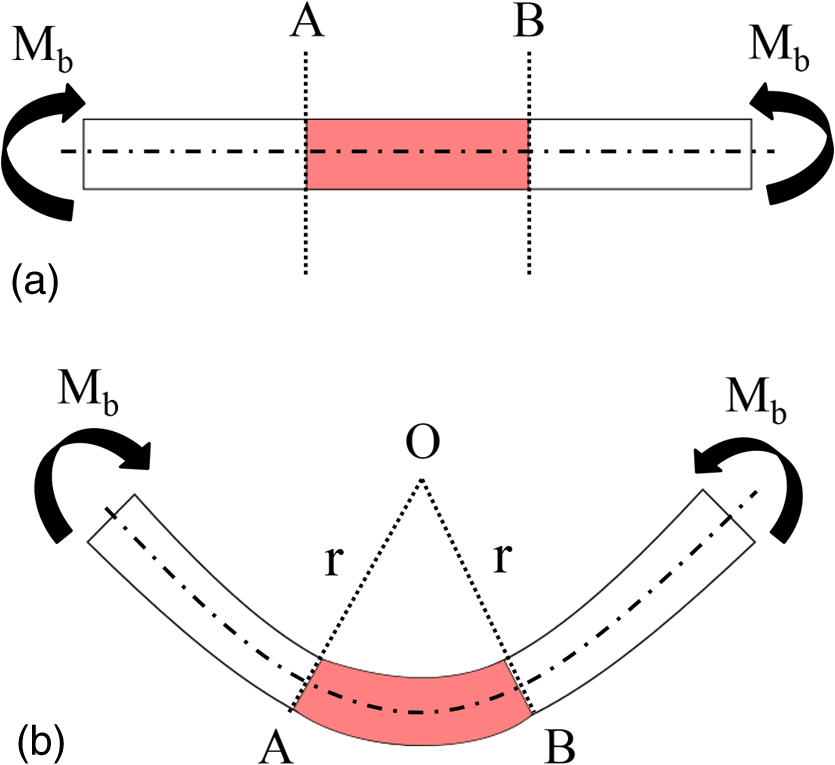
1.IntroductionTrends toward miniaturization require not only suitable fabrication technology of the systems at microscale, but also reliable measurement techniques for its physical properties. In this context, measurement systems are expected to provide more precise values in smaller unit. Force—as one of the most important physical parameters—plays an enormous role in technological advances of humankind, both in fundamental research and applications. Moreover, to determine small force precisely, appropriate sensors are needed. To date, several sensing mechanisms of sensors have been developed in recognizing small forces (e.g., changes of magnetic flux, capacitive, and piezoresistive). Mehrtash et al.1 developed a system utilizing a magnetic field to determine the environmental forces in the microdevice for human drug delivery. Meanwhile, polydimethylsiloxane-based force sensors also have been introduced utilizing the overlap between two electrodes on their top and bottom sides, which can detect forces in normal and tangential directions through the change of capacitance values.2 Hence, those flexible sensors were targeted for natural sensing mechanism with capability to measure weight and deflection of and , respectively. Nevertheless, transducing a mechanical into electrical signal by using the piezoresistive effect is still dominant in many sensing applications. Utilizing this effect, pressure sensors were fabricated and tested to determine sensitivity and linearity of different piezoresistive configurations at different temperatures.3 In this context, sensor design made of parallel transverse resistors has better sensitivity and linearity than a single transverse resistor. In contrast, two longitudinal strain gauges were integrated into a cantilever-based microforce sensor.4 The stress was applied on the free end of the beam structure with a length of , a width of , and a thickness of , which could be used for measuring forces on a microgripper. After calibration, this type of sensor demonstrated stiffness and sensitivity of and , respectively. Despite excellent sensitivity, the sensor was still too rigid, especially for applications in the fields of precision engineering (e.g., hardness measurement instruments, medical instruments, and micro-macro bilateral control). Furthermore, another application of use for a microforce sensor is the nanoindentation, which is basically a technique allowing mechanical characterization of materials by applying defined load or deflection onto the sample, so that its hardness can be determined.5 With the aim of broader force range and applications, depth sensing instruments have been successfully developed in the past to obtain a resolution of 1 nN and a displacement of . However, to ensure the highest quality of indentation instruments, reliable calibration procedures are still required, especially for lower force range application (i.e., systems with haptic force-feedback in minimal invasive surgery).6 Han et al.7 developed piezoresistive ring-shaped axial sensors to predict forces during catheterization. This sensor was attached on the tip on the guidewire and its movements in -direction led to deformation of the ring structure as well as the piezoresistive elements. Their thin resistors were fabricated on silicon-on-insulator (SOI) wafer, which showed a sensitivity value of in -direction. In addition to this, precise measurement of small forces is also useful for applications in robotics (e.g., macro-micro-bilateral control). Transfers of real-world haptic information (i.e., force and position) from microenvironment (target object) into the macrosurrounding (operator) are important for further development of medical technology.8 However, to realize this kind of operation control, the disturbances have to be taken into account. Mizutani and Katsura9 compensated the disturbances of the control system by integrating the saving and loading system within closed-loop operation. Furthermore, since the disturbances were also usually scaled, scaling rate is very important to determine whether the effect of the disturbances within a system can be neglected or not. Therefore, precise measurements of environmental reactions are needed to obtain the highest possible transparency, which can only be performed by compensating the disturbances.10,11 In this work, we proposed a stable microforce sensor based on double-layer (DL) SOI as transferable calibration standards. Unlike the similar calibration standard, our sensor was mainly fabricated employing an inductively coupled plasma (ICP) deep reactive ion etching (DRIE) process at cryogenic temperature.12 Therefore, anisotropy of the process can be controlled and integration of meander structures into the device is feasible. On both clamped ends, two piezoresistive strain gauges are used as active sensing elements. Therefore, the sensors have direct force-reading capability. To evaluate their performances, static and dynamic properties of the devices were characterized showing promising results to broaden their industrial applications (e.g., mechanical feedback control and robotics). 2.Sensor Design and Simulation2.1.Finite Element ModelingIn this initial effort, three different designs of SOI-based double-meander spring sensors were modeled, and an extensive micromechanical finite element modeling (FEM) was performed using COMSOL Multiphysics 4.3b.13 However, the interest of this study was to determine the impact of different design configurations to sensor characteristics (i.e., stiffness, linearity, and sensitivity). Considering the real sensor geometry, a three-dimensional (3-D) model was constructed instead of a simplified two-dimensional model. In general, the sensor consists of three main components: contact area in the center (boss), double spring structures flanking to the boss, and piezoresistive Wheatstone bridges (WBs) clamped on both ends of the chip [Figs. 1(a)–1(c)]. While the sensor spring was varied into three designs, the main area of the device was kept to be identical (i.e., ). Several different mesh sizes were manually chosen for different 3-D structures to save computational time without compromising any reliability of the simulation results.14 Moreover, single crystal anisotropic -doped silicon was chosen from the COMSOL library. The models were either rotated 45 deg in the -plane or a rotated coordinate system was defined using convention of Euler angle to perform simulation along 〈110〉 crystal orientation.13,15,16 Therefore, comparable physical properties with a fabricated sensor can be determined. Fig. 13-D finite element model of (a) the proposed silicon microforce sensor comprising (b) two identical etched WBs located close to the clamped ends and (c) the double-meander springs flanking to the boss. 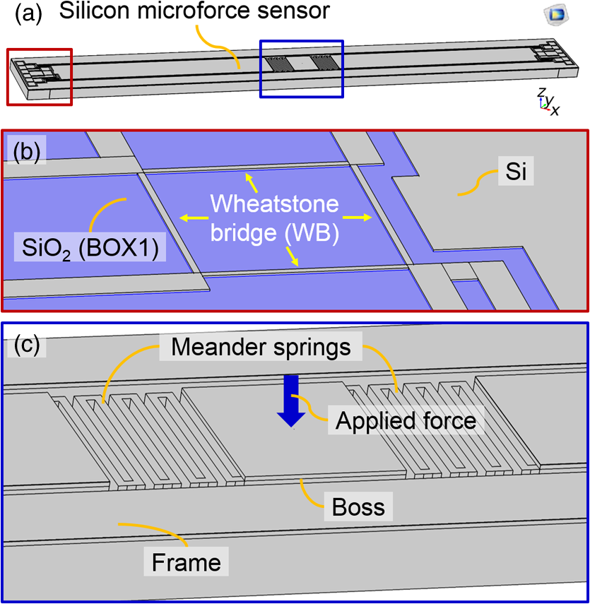 Meanwhile, mechanical and electrical properties of the devices were computed with two physics interfaces from the MEMS module, i.e., solid mechanics (solid) and piezoresistivity, domain currents (pzrd). All exterior mechanical boundaries of the sensor spring were set to be free, excluding the bottom part of the sensor frame, which was set to be fixed during force loading on the center part of the boss. For the electrical boundaries, an electrical potential of 1 V was applied to one of the electrode contacts from the WB as a dc input voltage (). Meanwhile, another contact electrode, which is diagonally aligned to the input electrode, was grounded. Thus, the offset voltages could be read from the other two diagonal nodes of the WB (). Three different sensor designs were differentiated by the shape of the spring structure close to the boss, although their total dimensions were kept equal (i.e., in length and in width). Perpendicular to -plane, design 1 has deep and small gap meander structures [Fig. 2(a)]. Compared to this, the spring design 2 has meander structures upright to the -plane or vertically aligned, which will require a more complex fabrication process to create such a rectangular corrugated surface profile [Fig. 2(b)]. On the other hand, the spring design 3 uses only simple thin membranes instead of meander structures as its spring component [Fig. 2(c)]. Fig. 2Three spring modifications of the enhanced microforce sensors showing (a) design 1 with horizontal meander structures on a flat surface profile, (b) design 2 with vertical meander structures on a rectangular corrugated surface profile, and (c) design 3 with flat rectangular plates fixed on the bottom of the boss.  2.2.Simulation Results on Device Stiffness and SensitivityThe numerical search of the optimal geometry configuration of the sensors is based on both mechanical and electrical properties (i.e., stiffness, nonlinearity, and sensitivity). The device models were assessed within the targeted application force range (i.e., between 0 and with a force increment of ). Deflection states of three different sensor designs under a force up to are shown in Fig. 4(a). Based on the assumption that the sensor elastically deforms and the origin of the coordinate system (, and ) is located on the clamping area of the neutral layer [Figs. 3(a)–3(b)], a point load applied on the boss structure induces a bending moment , which results in tensile stress in directions. The stress is distributed along the rectangular beam, which can be given as where , and are the distance from the neutral layer along the -axis, a certain position on the -axis, length, width, and thickness of the beam, respectively.17 In this case, WB structures are placed on the location where the highest mechanical stress is to be expected to occur, i.e., as far as possible from the applied force ( value should be minimum) and on the surface of the beam ( value should be ). Depending on Young’s modulus , the elongation may be expressed asConsidering the same deflection value, the stress can be quantified through the bending radius , which defines later the deformation of the WB structures and is accordingly determined as The force needed to obtain the same deflection value depends on the material, geometry, and bending properties, which is defined as and the stiffness is defined by the ratio of the applied force to the outcome deflection. where and are the applied load and boss deflection increments, respectively. Among the selected approaches, design 1 was evaluated to have the most compliant structure with a stiffness of , which is around 4.5 times smaller than that of design 2 (i.e., ). As expected for a membrane spring, the structure of design 3 has resulted in the highest stiffness value of [Fig. 4(b)]. In this case, the higher stiffness value indicates a more rigid behavior of the spring structure. Therefore, it can lead to better linearity of the force-deflection curves.Fig. 4(a) 3-D FEM results showing the conditions of three different designed microforce sensors under a force loading up to . The color legend describes the device displacement in micrometer scale. (b) Maximum displacements of their boss structure as a function of applied vertical force on its center position. Design 1 exhibits the most compliant structure among them. 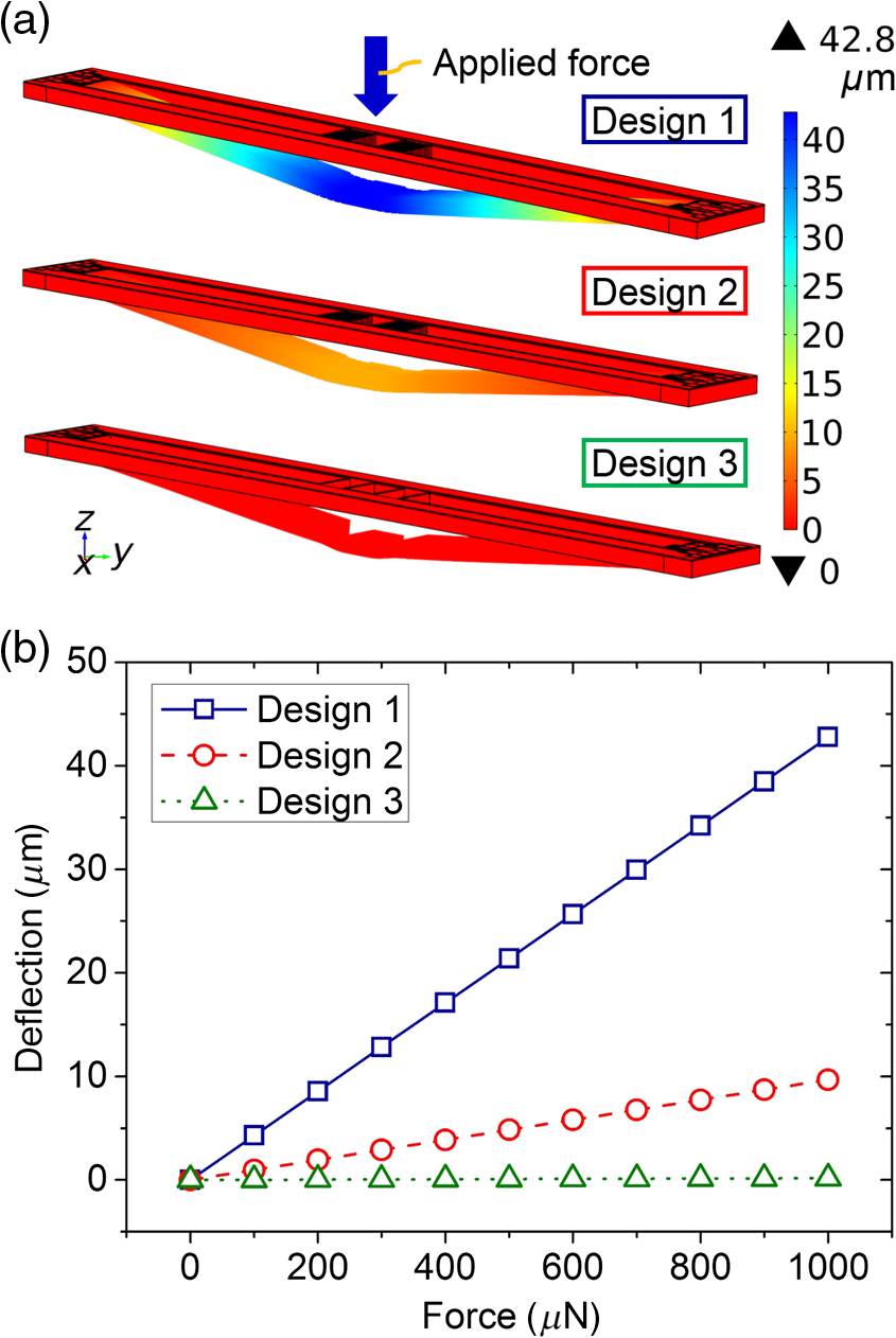 Apart from the stiffness and linearity, another essential quality characteristic of the device is sensor sensitivity. Because the output signal of the device is read using a piezoresistive method, the sensitivity in this circumstance is related to the WB performance. As a result, the sensitivity of a microforce sensor is defined to be the change in the WB resistance values (), which depends on the change of mechanical stress on the surface and the piezoresistive coefficient in longitudinal () and transverse directions (). In the simulation, these piezoresistive effects are directly represented as output voltages with regard to the change in the applied force.18 Moreover, doping concentrations on the WB and its electrical contact extensions are set to be and , respectively. Afterward, a supply voltage () of 1 V and the ground were applied through the diagonal opposite pads. Hence, the change of the output voltage () on the WB by different force loads can be measured, which is given as where , and are given resistor values corresponding to a full WB configuration. In Fig. 5(a), the distribution of voltage in the WB circuit under applied forces up to is presented. The sensitivity () is then calculated through the output voltage values () of different sensor architectures by different force loads ( to ) with an increment of , which can be defined asFig. 5(a) 3-D FEM results demonstrating the etched silicon piezoresistors designed in a full WB circuit under a force loading up to . The color legend describes the voltage distributed on the device structure in V-unit. (b) Sensor sensitivity of the sensors as a function of applied vertical force on its center position.  It is found that design 1 has the highest electromechanical sensitivity of , which is much higher than those of design 2 (i.e., ) and design 3 (i.e., ) by a factor of and , correspondingly [Fig. 5(b)]. Thus, design 1 can provide high sensor output voltages at relatively low applied forces. A comparison of the performed FEM of different sensor designs is shown in Table 1. These results suggest that design 1 with horizontal meander structures is superior to the other designs in terms of both stiffness and sensitivity with only relatively small standard deviation (). Therefore, design 1 has been chosen for the device fabrication. Table 1Simulation results of the microforce sensors with three different spring designs observed in the force range of 0 to 1000 μN.
3.Sensor Fabrication3.1.Fabrication Process StepsAfter engineering the designs and analyzing the simulation results, microforce sensors were fabricated to match the geometry of design 1. For this purpose, commercial -type DL-SOI wafers with orientation and a resistivity of the top layer of 0.01 to were used (Active Business Company GmbH, Germany). According to the manufacturer, the device, middle, and handle layers have thicknesses of , , and , respectively. Between those silicon layers, two isolation layers of buried oxides (i.e., BOX1 and BOX2), which are located on the upper and lower positions, possess thicknesses of and , respectively. The physical parameters of the wafer are summarized in Table 2. Table 2Material specification of the DL-SOI used for meander spring microforce sensors.
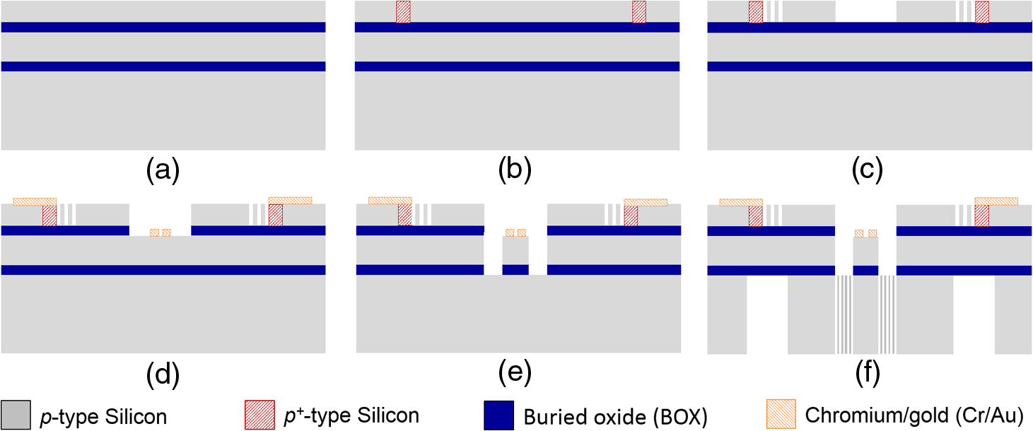
Sensor fabrication was conducted based on silicon bulk micromachining processes. The key fabrication steps are schematically shown in Fig. 6, which can be described in detail as follows:
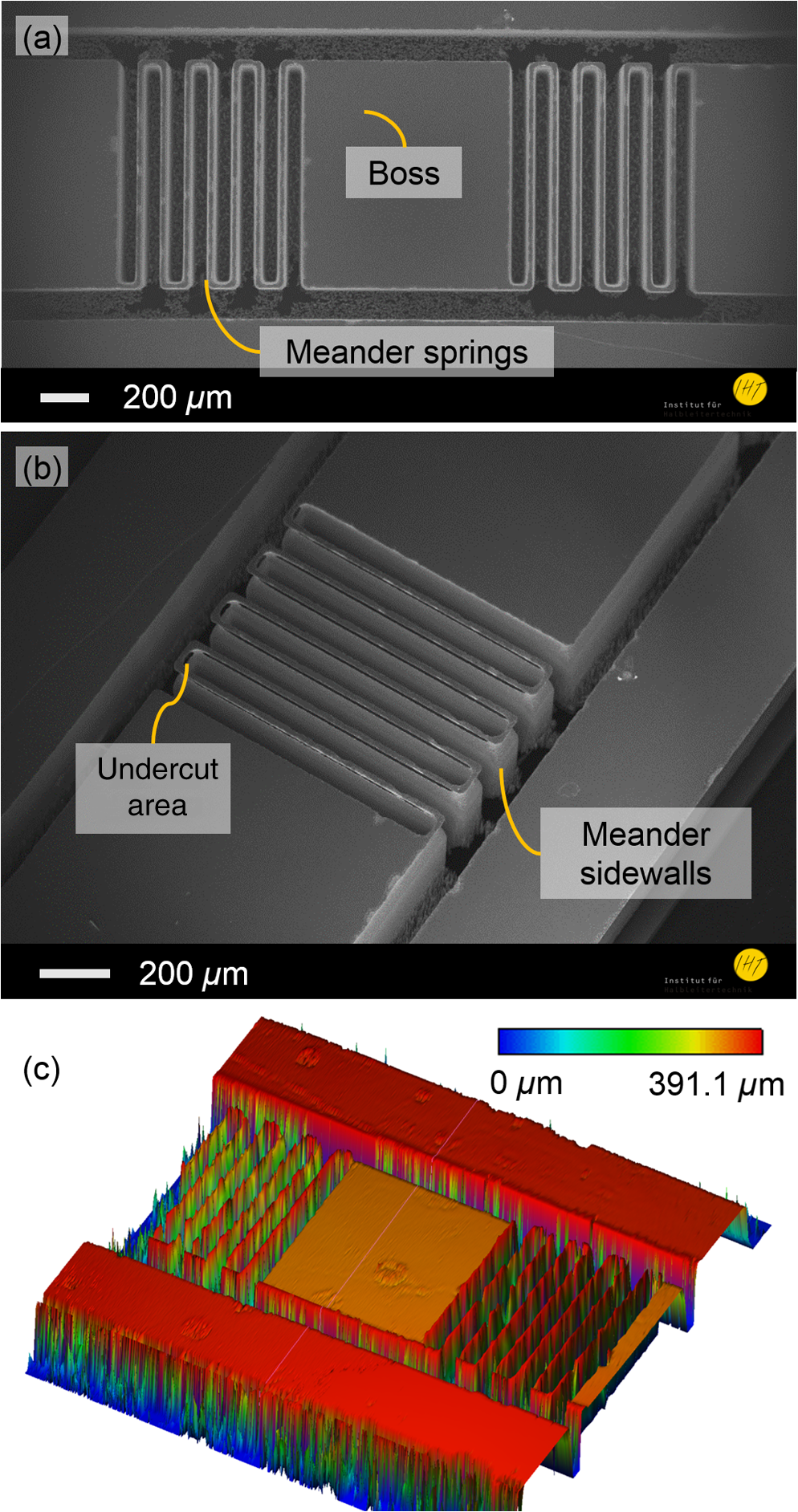
3.2.Fabricated Active Microforce SensorsAfter being released from the fabrication batch, the large samples were then diced into six single piezoresistive-based microforce sensing devices [i.e., each sensor has a dimension of , see Fig. 7(a)] by taking the advantage of an annexed thin membrane located to one of the sensor frame sides. Thus, in this case, a tweezer can be used instead of a more complicated and expensive dicing blade tool to separate the sensors from the dies. The sensors were then taken to be examined optically in a scanning electron microscope (SEM). On both ends of the front side, WBs as active sensing elements were created to characterize mechanical tension during material deformation [Fig. 7(b)]. These locations close to clamped ends are expected to have the maximum stress levels along the sensor beam length, which have been proven from FEM (i.e., to for an applied force of 1 mN). The conversion of the material deformation into an electrical signal was carried out by the implemented piezoresistive mechanism. Moreover, the design of full -type WBs may have better performance with regard to temperature effect cancellation compared to a half-bridge circuit. Meanwhile, for their vertical thickness, the fabricated resistors exhibit very high uniformity attributed to the predefined SOI-material thickness. This would be beneficial compared to the conventional diffused or implanted -type resistors on -type substrates for better designing and controlling the precise resistance values of the piezoresistors (i.e., in the range of ).19,20 Therefore, we could obtain well-defined perpendicularly arranged resistors [Fig. 7(c)]. However, it should also be noted that the oxide areas surrounding the bridge had been extended compared to the former design (i.e., ) to avoid unwanted micro/nanoparticles shorting the active silicon regions.21 This phenomenon could either occur during wire bonding or sensor characterization. Fig. 7(a) Optical and (b) scanning electron microphotographs of the fabricated active silicon microforce sensors showing (c) the etched piezoresistive WB structures at the sensor clamped end. 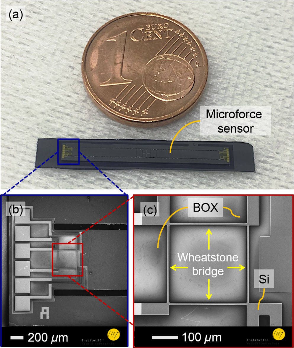 In addition to the WB structures, we also characterized the fabricated spring structures on the device optically. Figure 8(a) shows the boss and both clamped meander spring structures viewed from the bottom side. Although there were some imperfections of the overetched areas on the structures, which might be caused by nonuniform temperature distribution during the etch process, these meander structures were still expected to be able to improve the sensor performance [Fig. 8(b)]. Another possible reason for this case was the used self-bias set by the high-frequency power. Nevertheless, this type of artifact could be reduced or even eliminated by better adjustment of the etch recipe. Hence, smoother trench sidewalls as well as more uniform silicon blocks could be obtained.21,22 Furthermore, a 3-D laser microscope (LEXT OLS4000 3D Laser Measuring Microscope, OLYMPUS) was used to measure the meander actual geometry and its surface profile after fabrication. It can be obviously seen from the extracted 3-D micrograph [Fig. 8(c)] that although the meander structures show good uniformity and perpendicular walls on their structure, their actual size has been shrunk to be smaller than designed and modeled geometry (i.e., from 50 to ), which may affect the performance of the sensors, especially for their stiffness. 3.3.Piezoresistive Wheatstone BridgesThe dimensions (i.e., width and thickness) of the fabricated WB structures are measured using SEM and a 3-D laser microscope. The full image of the WB and its magnification of several critical positions were captured and analyzed (s. Fig. 9). The measured width single resistor geometry exhibits very low deviation () for the investigated WBs with an average value of . As a consequence, the offset voltage of the fabricated WBs was also low (i.e., expected to be ). Ideally, the offset voltage should be zero. However, due to imperfections of fabrication processing steps, such small values in practical situations can still be acceptable for signal processing of the piezoresistive sensors. Fig. 9SEM images of the fabricated etched -SOI WB with its magnified views on its middle and corner parts for quality inspection from optical measurements. 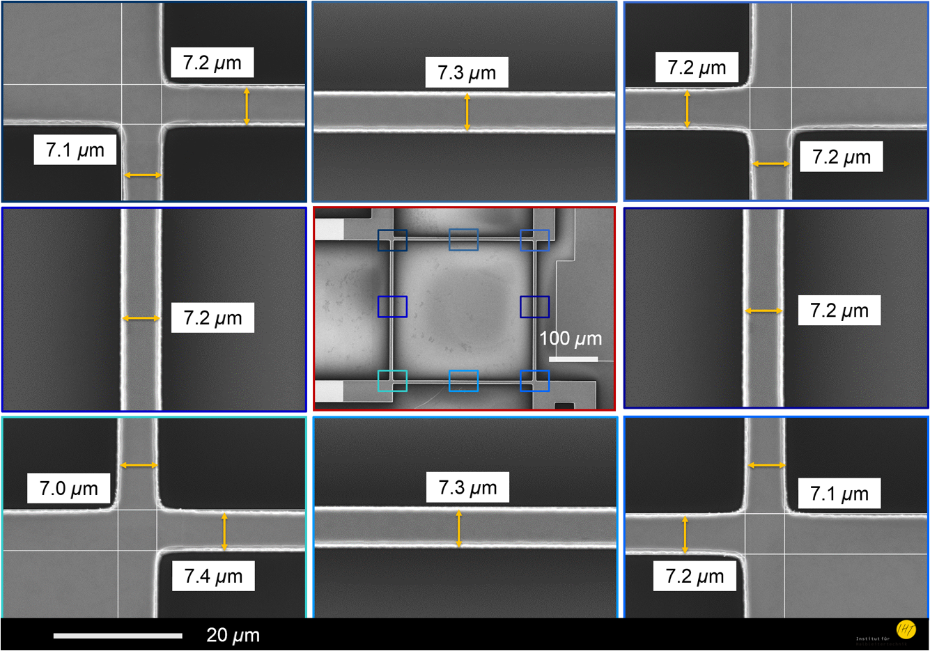 Moreover, two neighboring WB structures, which are located next to each other at 90 deg angle, were measured by a 3-D laser microscope [Figs. 10(a)–10(c)]. The functional structure under line A is by narrower than that under line B. In addition, the structure under line A has a height of compared with the structure under line B of , which are within the manufacturing tolerance of the DL-SOI device layer (i.e., ). It should be noted that the measurements were also performed for the other three corners of the WB, which yielded similar results as the described one. These values demonstrate that the geometry deviation during the etching was relatively small with maximum values of 0.1 and in vertical and horizontal directions, respectively. Therefore, the etch recipe can be used to reproducibly fabricate etched WBs with structure dimensions matching that of the employed lithography mask. Fig. 10(a) One corner of the etched WB under test in 3-D laser microscope showing two cross section lines (i.e., lines A and B) to characterize (b) the width and (c) the height of the piezoresistor structures.  In this work, two different metallization forms were applied on the devices (i.e., full- and half-metal contacts). The full metal type covers the whole electrical path surfaces from the contact pads to the WB corners [Fig. 11(a)]. For the half-metal contact, the Cr/Au layer was deposited only on the top of a defined area outside the membrane [Fig. 11(b)]. This second metallization design was made considering the avoidance of an additional stress from full metal on the thin membrane area where the WB was located. However, the implementation of different metallization designs has consequences on the wire resistance values, which can be determined from the measured resistance values between contacts 2 and 3 as well as 5 and 6, i.e., and . In Table 3, the measured resistances , and are listed. As expected, higher values were observed with half-metal stripes owing to the higher wire resistance. However, the offset values of both options, which were reasonably low in both cases (i.e., ), showed much lower values for the half-metal stripes ( and for left and right WBs, respectively) than the full-metal stripes. Therefore, regardless of the slight deviations of the fabricated WB geometries from an ideal cuboid shape, reliable output signals still can be expected in all cases. Fig. 11Optical micrographs of the piezoresistive etched WBs with (a) full- and (b) half-metal contacts. 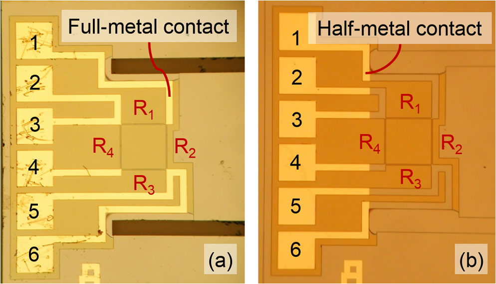 Table 3Electrical properties different metallization type.
4.Sensor Characterizations4.1.Sensor Static ResponseFollowing the optical and electrical characterizations of the WB, sensors were then further tested in force-loading measurements for investigating its mechanical properties and to confirm the benefits of the engineered meander springs, as it would be used as a microforce calibration standard. Moreover, to guarantee constant temperature, humidity, and pressure during the measurement as well as to eliminate measurement errors caused by environmental issues, the sample was placed inside a controlled chamber imitating normal laboratory conditions (, ). Figures 12(a) and 12(b) show the device under test, where the silicon microforce sensor was fixed on an aluminum block holder, which could be moved in 3-axis directions. Precise positioning of this part was secured by a nanopositioner with a resolution of 1 nm and a maximum displacement of .23 The applied forces were measured by a compensation balance through a ruby sphere with a diameter of as the mechanical contact element. In this study, the force was limited to to avoid overloading the structure. Meanwhile, the measured data acquisition was performed in every 400 nm steps of -direction (i.e., parallel to the loading shaft). It is crucial to ensure linear beam behavior within the sensor operating range, because at a certain point too high applied forces may cause nonlinear force-deflection curve as well as device fracture. Figure 12(c) exhibits a typical measured position-force curve of a microforce sensor and its first and second derivatives, which exhibit very good linearity with increasing force. Fig. 12Photographs of (a) the microforce sensor under test using (b) a microshaft attached with a stylus ball for applying force on the center of the boss. (c) Measurement results in the force range of 0 to showing linear profile. 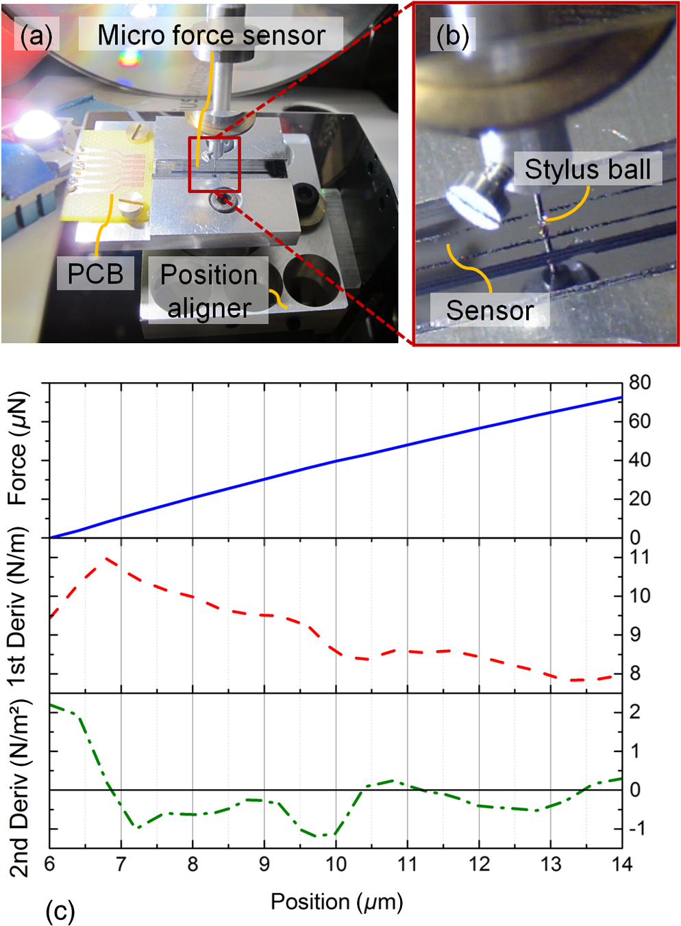 The mechanical measurements were then repeated for 24 times to observe the sensor stability as well as to have quantitative measurement data. Hence, the device properties can be reliably extracted from the measured values. Moreover, to investigate its hysteresis behavior, the sensor monitoring was performed in both conditions of increasing and decreasing force loadings. The increasing loading started from the initial contact between the stylus ball and the boss, in which the shaft then further pushed the sensor toward its lower position. Similarly, the decreasing loading (i.e., unloading) was captured when the loading shaft had started to be pulled up toward its higher position. In these measurements, we determined three critical parameters, i.e., device stiffness, force sensitivity, and bending sensitivity. Figures 13(a) and 13(b) show the measured device stiffness in the force range from 1 to during loading (i.e., ) and unloading (i.e., ) conditions, respectively. These measured stiffness values are almost three times lower than that of FEM (i.e., ), which can be attributed to the overetching of the meander springs leading to a stiffness reduction [Fig. 8(c)]. Furthermore, some parts of the meander structures were not completely released, causing a reduction of the stiffness. On the other hand, the measured sensitivity values of the sensor with respect to the bending forces are and during loading and unloading of the shaft, respectively [Figs. 13(c) and 13(d)]. It is also interesting to determine the bending sensitivity. From Figs. 13(e) and 13(f), it is found that their measured values are in the ranges of and for loading and unloading conditions, respectively. All in all, the measurement values for those three parameters of the sensor mechanical properties have exhibited very small hysteresis (), confirming the performance consistency and device stability on both loading and unloading characterizations. Fig. 13Repeated measurements at one loading position on the center of the boss showing the small differences of [(a) and (b)] stiffness, [(c) and (d)] force sensitivity, and [(e) and (f)] bending sensitivity in loading and unloading conditions, respectively. 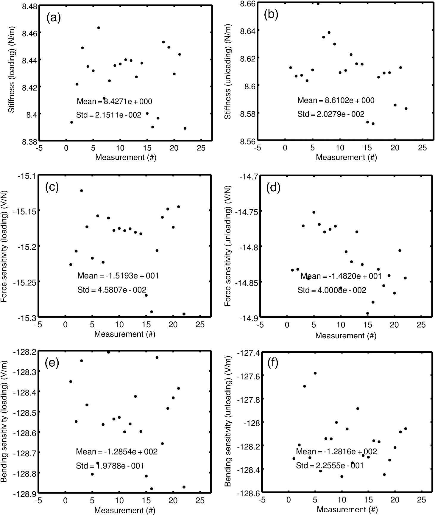 Additionally, the performance of the fabricated double-meander force sensors is evaluated by direct comparison of their experimental and simulation results (Table 4). For the stiffness, the final fabricated device has a lower mean value of , which is almost half that of the FEM. In contrast, the mean fabricated sensor sensitivity yields higher mean value than the FEM results (i.e., ). Regardless of the required fabrication optimizations (e.g., improved etching process and spring designs), a combination of low stiffness and high sensitivity compared with the FEM solutions is beneficial for precise measurement procedures of very low forces. Table 4Comparison of device properties (numerical analysis versus fabricated device).
4.2.Sensor Dynamic ResponseIn addition to the static response of the sensor, two real-time measurements (i.e., with constant and varied transverse loading speeds) were carried out to evaluate the dynamic response of the device, which is particularly exciting for robotics or automated systems based applications. In the first experiment, the signal of WB of the force sensor was monitored at the initial state, where there was no contact between the stylus and the device. Once the stylus had moved downward onto the sensor contact area and loaded the sensor with a defined velocity of and a force of , a maximum deflection of could be obtained. At this stage, the signal was measured within and its average value was calculated to investigate the stability of the sensor under loading condition [Fig. 14(a)]. Afterward, the stylus was released to its initial position and reached its stable condition by experiencing an oscillation [Fig. 14(b)]. The output voltage without and with contact loadings are and , respectively. After repeating the measurements three times, similar values of the output voltage during contact are obtained, confirming the reproducibility and reliability of the device. Furthermore, from the flexural frequency measurement, the device has a fundamental resonant frequency of 805 Hz [Fig. 14(c)]. Fig. 14Repeated dynamic measurements of microforce sensor to determine at [(a) and (b)] constant loading speed, (c) fundamental resonance, and (d) sequentially increasing loading velocity. 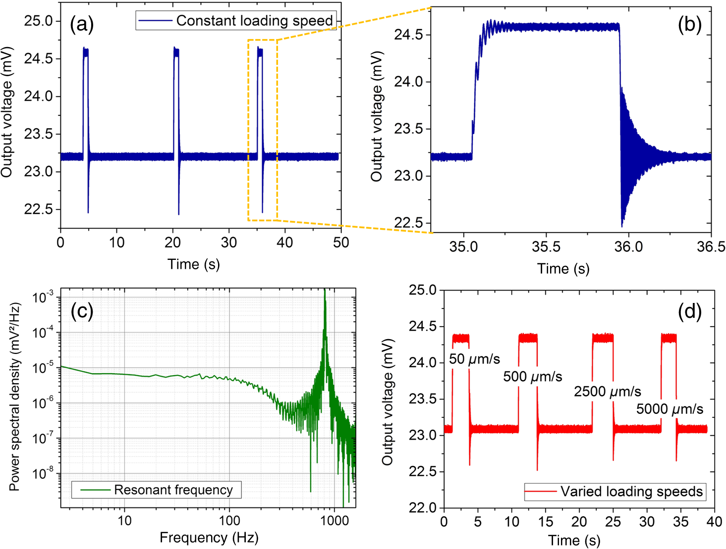 For the second dynamic loading measurement, the sensor was tested in different loading velocities to justify its rapid responses concerning the real applications, where the forces can be applied in various speeds. However, it should be noted that the system configuration and measurement method were kept identical as those of the first measurement. From Fig. 14(d), the initial offset voltage value was in the condition of no contact. Under traverse speed of , the output voltage in loading position was . Although the indentation speed during loading and unloading sequences had been increased sequentially (i.e., 500, 2500, and ), the output signal of the force sensor had shown similar behavior as the one measured at the lowest speed (i.e., ). This could be seen from the calculated deviations of those four different output signals, which showed a very small value of . Based on these results, the device can be considered to be potentially used to rapidly detect mechanical signal and transduce it directly into an electrical signal with stable and reliable performances. 5.ConclusionPiezoresistive silicon microforce sensors as a transferable calibration standard have been developed by optimizing the mechanical (i.e., springs) and electrical readout elements (i.e., piezoresistors). The meander spring design was chosen among others for fabrication because of its superior properties (i.e., lower stiffness and higher sensitivity) obtained using FEM. A particular wafer of DL-SOI has been used instead of a bulk silicon wafer to ensure very well-defined dimensions of the boss, springs, and WBs. The experimental results showed that the fabricated sensors have very good stability and properties in repeated mechanical force measurements, although their values are slightly different from those predicted by FEM. Regardless of the shown promising performance, some further experiments and optimizations are required to better justify the sensor functionality and obtain higher linearity and sensitivity. AcknowledgmentsThe authors thank Juliane Arens and Doris Rümmler for their technical support. The first author gratefully acknowledges support by Braunschweig International Graduate School of Metrology (B-IGSM). This work was performed in the collaborative project “HmtS” funded by the German Federal Ministry of Education and Research (BMBF) under No. 03V0307. ReferencesM. Mehrtash et al.,
“Bilateral magnetic micromanipulation using off-board force sensor,”
IEEE/ASME Trans. Mechatron., 20
(6), 3223
–3231
(2015). http://dx.doi.org/10.1109/TMECH.2015.2417116 Google Scholar
L. Viry et al.,
“Flexible three-axial force sensor for soft and highly sensitive artificial touch,”
Adv. Mater., 26
(17), 2659
–2664
(2014). http://dx.doi.org/10.1002/adma.201305064 ADVMEW 0935-9648 Google Scholar
S. S. Kumar and B. D. Pant,
“Effect of piezoresistor configuration on output characteristics of piezoresistive pressure sensor: an experimental study,”
Microsyst. Technol., 22
(4), 709
–719
(2015). http://dx.doi.org/10.1007/s00542-015-2451-5 0946-7076 Google Scholar
B. Komati et al.,
“Prototyping of a highly performant and integrated piezoresistive force sensor for microscale applications,”
J. Micromech. Microeng., 24
(3), 035018
(2014). http://dx.doi.org/10.1088/0960-1317/24/3/035018 JMMIEZ 0960-1317 Google Scholar
A. M. Díez-Pascual et al.,
“Nanoindentation in polymer nanocomposites,”
Prog. Mater. Sci., 67 1
–94
(2015). http://dx.doi.org/10.1016/j.pmatsci.2014.06.002 PRMSAQ 0079-6425 Google Scholar
M. C. Yip, S. G. Yuen and R. D. Howe,
“A robust uniaxial force sensor for minimally invasive surgery,”
IEEE Trans. Biomed. Eng., 57
(5), 1008
–1011
(2010). http://dx.doi.org/10.1109/TBME.2009.2039570 IEBEAX 0018-9294 Google Scholar
B. Han et al.,
“Silicon nanowire-based ring-shaped tri-axial force sensor for smart integration on guidewire,”
J. Micromech. Microeng., 24
(6), 065002
(2014). http://dx.doi.org/10.1088/0960-1317/24/6/065002 JMMIEZ 0960-1317 Google Scholar
P. S. Girao et al.,
“Tactile sensors for robotic applications,”
Measurement, 46
(3), 1257
–1271
(2013). http://dx.doi.org/10.1016/j.measurement.2012.11.015 Google Scholar
Y. Mizutani and S. Katsura,
“Disturbance compensation based on data memory for macro–micro bilateral control,”
in IEEE Int. Symp. on Industrial Electronics,
(2013). http://dx.doi.org/10.1109/ISIE.2013.6563728 Google Scholar
Y. Mizutani and S. Katsura,
“Analysis, modeling, and compensation of friction for scaled bilateral control,”
IEEE J. Ind. Appl., 3
(4), 344
–349
(2014). http://dx.doi.org/10.1541/ieejjia.3.344 Google Scholar
A. M. Ousaid et al.,
“A stable and transparent microscale force feedback teleoperation system,”
IEEE/ASME Trans. Mechatron., 20
(5), 2593
–2603
(2015). http://dx.doi.org/10.1109/TMECH.2015.2423092 IATEFW 1083-4435 Google Scholar
J. Frühauf et al.,
“Calibration of instruments for hardness testing by use of a standard,”
in Recent Advancement of Theory and Practice in Hardness Measurement, Proc. HARDMEKO,
141
–145
(2007). Google Scholar
COMSOL Multiphysics Release Notes: Version 4.3b, Stockholm, Sweden
(2013). https://www.comsol.de/shared/downloads/4.3b/ReleaseNotes.pdf Google Scholar
H. S. Wasisto et al.,
“Finite element modeling and experimental proof of NEMS-based silicon pillar resonators for nanoparticle mass sensing applications,”
Microsyst. Technol., 20
(4–5), 571
–584
(2014). http://dx.doi.org/10.1007/s00542-013-1992-8 0946-7076 Google Scholar
M. A. Hopcroft, W. D. Nix and T. W. Kenny,
“What is the Young’s modulus of silicon?,”
J. Microelectromech. Syst., 19
(2), 229
–238
(2010). http://dx.doi.org/10.1109/JMEMS.2009.2039697 JMIYET 1057-7157 Google Scholar
I. Bonev and D. Zlatanov,
“Advantages of the modified Euler angles in the design and control of PKMs,”
in Proc. 3rd Chemnitz Parallel,
199
–216
(2002). Google Scholar
S. J. Park et al.,
“Piezoresistive cantilever performance—part I: analytical model for sensitivity,”
J. Microelectromech. Syst., 19
(1), 137
(2010). http://dx.doi.org/10.1109/JMEMS.2009.2036581 JMIYET 1057-7157 Google Scholar
J. C. Doll and B. L. Pruitt,
“Microsystems and nanosystems,”
Piezoresistor Design and Applications, 1 Springer, New York
(2013). Google Scholar
H. S. Wasisto et al.,
“Handheld personal airborne nanoparticle detector based on microelectromechanical silicon resonant cantilever,”
Microelectron. Eng., 145 96
–103
(2015). http://dx.doi.org/10.1016/j.mee.2015.03.037 MIENEF 0167-9317 Google Scholar
H. S. Wasisto et al.,
“Portable cantilever-based airborne nanoparticle detector,”
Sens. Actuators B, 187 118
–127
(2013). http://dx.doi.org/10.1016/j.snb.2012.09.074 Google Scholar
H. S. Wasisto et al.,
“Development of silicon microforce sensors integrated with double meander springs for standard hardness test instruments,”
Proc. SPIE, 9517 95171X
(2015). http://dx.doi.org/10.1117/12.2180117 PSISDG 0277-786X Google Scholar
S. Merzsch et al.,
“Silicon based sensors and functional components fabricated by ICP-RIE cryogenic dry etching,”
in 23rd Micromechanics Microsystems European Workshop,
3
–6
(2012). Google Scholar
PI Datasheet P-721, Nanopositioning device with digital controller, Karlsruhe, Germany
(2014). http://www.physikinstrumente.com/download/PI_DataSheet_P-721_42034.pdf. Google Scholar
BiographyGerry Hamdana received his BEng degree in mechanical engineering from the Esslingen University of Applied Science in 2012 and his MSc degree in mechanical engineering specializing in mechatronic/microsystems technology from the Braunschweig University of Technology (TU Braunschweig), Germany, in 2015. Currently, he is pursuing his PhD at the Institute of Semiconductor Technology (IHT), TU Braunschweig, Germany. His research interests include semiconductor micro/nanostructuring, silicon micro/nanomachining, and micro/nanoelectromechanical systems (MEMS/NEMS). Hutomo Suryo Wasisto received Dr-Ing degree in electrical engineering, information technology, and physics with summa cum laude honor from the TU Braunschweig, Germany, in 2014. He was a postdoctoral fellow at Georgia Institute of Technology, Atlanta, from 2015 to 2016. Currently, he is head of the Optoelectromechanical Integrated Nanosystems for Sensing (OptoSense) Group in the Laboratory for Emerging Nanometrology (LENA), Braunschweig, Germany. His main research interests include nano-opto-electro-mechanical systems (NOEMS), nanosensors, nanoelectronics, and nanometrology. Lutz Doering received his Dr.-Ing. degree in microelectronics technology, precision instrument technology, and computer science from the Dresden University of Technology, Dresden, Germany, in 1990. He joined the Department 5.1 Nano- and Micrometrology, Physikalisch-Technische Bundesanstalt (PTB), Braunschweig, Germany, in 2001. His current research interests include characterization and optimization of micromachined cantilever sensors designed for measuring coordinate and roughness parameters and for the transfer of the micronewton and nanonewton force standard to tactile probing tools. Chunlei Yan received his Bachelor of Science degree in integrated circuit design and integrated systems from Xidian University, China, in 2012. Currently, he is pursuing his master’s degree in electrical engineering at the Braunschweig University of Technology (TU Braunschweig), Germany. Lei Zhou received her bachelor’s degree in electronic science and technology from Xidian University, China, in 2013. Currently, she is pursuing her master’s degree focusing on nanosystems engineering at the Braunschweig University of Technology (TU Braunschweig), Germany. Uwe Brand received his PhD in physics from the TU Braunschweig, Germany, in 2000. Since, 2010 he has been the head of working group 5.11 hardness and tactile probing methods in Physikalisch-Technische Bundesanstalt (PTB), Braunschweig, Germany. His main research interests include the development of the nanoindentation technique and standard devices. His research group creates the basis for the traceability of hardness measurements in industry, research institutes, and calibration laboratories. Erwin Peiner received his PhD in metastable binary metal compounds by ion beam mixing from the University of Bonn, Bonn, Germany, in 1988, and the Venia Legendi degree in semiconductor technology from the Faculty of Mechanical and Electrical Engineering, TU Braunschweig, Braunschweig, Germany, in 2000. Currently, he is the leader and professor of the Semiconductor Sensors and Metrology Group, IHT. He is the project coordinator of the collaborative project “HmtS” funded by the BMBF. |
||||||||||||||||||||||||||||||||||||||||||||||||||||||||||||||||||||||||||||||||||||||||||||